Microlenses Optical Cavities and Light Extraction in MicroLED Design
AUG 25, 202510 MIN READ
Generate Your Research Report Instantly with AI Agent
Patsnap Eureka helps you evaluate technical feasibility & market potential.
MicroLED Light Extraction Technology Background and Objectives
MicroLED technology has emerged as a promising next-generation display technology, offering advantages in brightness, energy efficiency, and form factor flexibility. The evolution of this technology can be traced back to the early 2000s when the first micro-scale LED devices were demonstrated in research laboratories. Since then, significant advancements have been made in materials science, fabrication techniques, and integration methods, propelling MicroLED from a laboratory curiosity to a commercially viable display technology.
Light extraction efficiency represents one of the most critical challenges in MicroLED development. Historically, conventional LED technologies have suffered from total internal reflection phenomena, where a substantial portion of generated light remains trapped within the semiconductor material due to the significant refractive index mismatch between the LED material and air. This fundamental optical limitation has driven continuous innovation in light management strategies.
The technological trajectory of MicroLED light extraction has evolved through several distinct phases. Initially, simple surface roughening techniques were employed to disrupt total internal reflection. This was followed by the introduction of more sophisticated approaches including photonic crystals, distributed Bragg reflectors, and most recently, advanced microlens arrays and engineered optical cavities. Each evolutionary step has incrementally improved extraction efficiency, though significant challenges remain.
Current industry benchmarks indicate that commercial MicroLED displays typically achieve light extraction efficiencies between 20-40%, representing substantial room for improvement compared to the theoretical maximum. This efficiency gap translates directly to increased power consumption, reduced brightness, and ultimately higher production costs for MicroLED displays.
The primary technical objective in this domain is to develop scalable, cost-effective light extraction solutions that can achieve extraction efficiencies exceeding 70% while maintaining compatibility with mass production processes. This involves optimizing the design of microlenses to effectively redirect light that would otherwise be trapped, engineering optical cavities to enhance directional emission, and developing novel materials with optimized optical properties.
Additionally, as MicroLED pixel sizes continue to shrink below 10 microns for high-resolution applications, conventional light extraction approaches face new challenges related to diffraction limits and near-field optical effects. Therefore, another critical objective is to develop extraction techniques that remain effective at these ultra-small dimensions, potentially leveraging nanophotonic principles and metamaterial concepts.
The successful development of advanced light extraction technologies for MicroLED will directly impact key performance metrics including power efficiency, brightness, and production yield, ultimately determining the technology's competitiveness against established display technologies like OLED and LCD in consumer electronics markets.
Market Analysis for MicroLED Display Applications
The MicroLED display market is experiencing unprecedented growth, driven by the technology's superior performance characteristics compared to traditional display technologies. Current market projections indicate that the global MicroLED market is expected to reach $20.5 billion by 2026, growing at a CAGR of 89.3% from 2021. This explosive growth is fueled by increasing demand for brighter, more energy-efficient displays with higher resolution and contrast ratios.
Consumer electronics represents the largest application segment for MicroLED technology, with smartphones, smartwatches, and AR/VR headsets leading adoption. Apple's acquisition of LuxVue and subsequent patents related to MicroLED technology signals strong interest from major industry players. Samsung and Sony have also made significant investments in MicroLED development, particularly for large-format displays and television applications.
The automotive sector presents another rapidly expanding market for MicroLED displays. Advanced driver-assistance systems (ADAS) and in-vehicle infotainment systems require high-brightness displays that can operate reliably in varying lighting conditions. MicroLED's superior brightness, which can exceed 1,000,000 nits, makes it particularly suitable for automotive applications, with market penetration expected to grow by 76% annually through 2025.
Healthcare and medical applications represent an emerging but promising segment. The high resolution and color accuracy of MicroLED displays make them ideal for medical imaging and diagnostic equipment. This segment is projected to grow at 65% annually as healthcare facilities upgrade to more advanced visualization technologies.
Regional analysis reveals that Asia-Pacific currently dominates MicroLED manufacturing, with Taiwan, South Korea, and China accounting for approximately 68% of global production capacity. North America leads in technology development and intellectual property, while Europe focuses on specialized applications in automotive and industrial sectors.
Market challenges include high manufacturing costs and low yield rates, particularly related to the mass transfer process of individual LED elements. Current manufacturing costs for MicroLED displays are 4-5 times higher than comparable OLED displays, limiting mass-market adoption. However, innovations in optical design, including microlenses and optimized light extraction techniques, are expected to improve efficiency and reduce costs by up to 40% within the next three years.
Consumer demand for higher resolution displays with lower power consumption continues to drive market growth. The average power efficiency improvement of 30-50% offered by MicroLED over OLED technology represents a significant competitive advantage, particularly for battery-powered devices where energy consumption is critical.
Current Challenges in MicroLED Optical Efficiency
MicroLED technology represents a significant advancement in display technology, offering superior brightness, contrast, and energy efficiency compared to traditional LED and OLED displays. However, the optical efficiency of MicroLEDs remains a critical challenge that limits their widespread commercial adoption. Current MicroLED designs face substantial light extraction inefficiencies, with internal quantum efficiency often reaching only 20-30% of theoretical maximums.
The primary challenge stems from the fundamental physics of light propagation in semiconductor materials. Due to the high refractive index contrast between the LED semiconductor material and the surrounding medium (typically air), total internal reflection traps a significant portion of generated light within the device structure. This phenomenon, known as the "light escape cone" limitation, prevents approximately 70-80% of generated photons from being extracted.
Another significant challenge is the miniaturization paradox: as MicroLED dimensions decrease to achieve higher pixel densities, the surface-to-volume ratio increases, exacerbating surface recombination effects. These non-radiative recombination processes at surface defects reduce internal quantum efficiency, particularly in blue and green MicroLEDs where the effect is most pronounced.
Current manufacturing processes introduce additional optical efficiency challenges. The etching processes used to define individual MicroLED pixels create sidewall defects that act as non-radiative recombination centers. These defects become increasingly significant as pixel sizes decrease below 10 micrometers, creating a fundamental scaling limitation for high-resolution displays.
The integration of optical structures such as microlenses and optical cavities presents its own set of challenges. While these elements can theoretically improve light extraction, their fabrication at the microscale requires precise alignment and consistent optical properties. Current manufacturing techniques struggle to achieve the necessary precision at commercially viable yields, particularly for mass-production scenarios.
Color conversion layers, essential for creating full-color displays from primarily blue MicroLED emitters, introduce additional optical interfaces that can trap or scatter light. The quantum efficiency of color conversion materials (typically quantum dots or phosphors) rarely exceeds 90%, creating another efficiency bottleneck in the optical path.
Heat management represents another critical challenge affecting optical efficiency. As current densities increase in smaller MicroLEDs, localized heating can lead to thermal quenching effects that reduce quantum efficiency. This creates a complex optimization problem where electrical efficiency, thermal management, and optical performance must be balanced simultaneously.
Industry benchmarking reveals that current commercial MicroLED prototypes achieve external quantum efficiencies of approximately 15-25%, significantly lower than the theoretical maximum of 70-80%. Bridging this efficiency gap represents one of the most pressing challenges for enabling widespread MicroLED adoption across consumer electronics, automotive displays, and augmented reality applications.
Microlenses and Optical Cavity Design Solutions
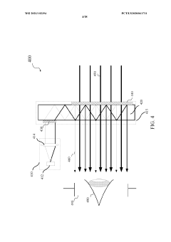
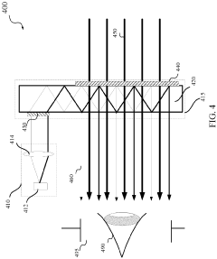
01 Microlens arrays for light extraction enhancement
Microlens arrays can be integrated on the surface of MicroLED devices to enhance light extraction efficiency. These arrays redirect light that would otherwise be trapped due to total internal reflection, allowing more photons to escape from the device. The microlenses can be fabricated using various materials and techniques, including photolithography and etching processes, and can be optimized in terms of shape, size, and arrangement to maximize light extraction for specific MicroLED configurations.- Microlens arrays for light extraction enhancement: Microlens arrays can be integrated on the surface of MicroLED devices to significantly improve light extraction efficiency. These arrays redirect light that would otherwise be trapped due to total internal reflection at the semiconductor-air interface. The microlenses can be fabricated using various materials and techniques, including photolithography and etching processes, and can be designed with specific shapes and arrangements to optimize the extraction of light from different regions of the MicroLED.
- Optical cavity design for MicroLED efficiency: Optical cavities in MicroLED structures can be engineered to enhance light extraction by controlling the resonance conditions and directing emitted light. These cavities can be formed using distributed Bragg reflectors (DBRs), metal reflectors, or other reflective structures that create constructive interference patterns. By optimizing the cavity dimensions and materials, the directionality and intensity of emitted light can be significantly improved, leading to higher external quantum efficiency.
- Surface texturing and nanostructures for light extraction: Surface texturing and nanostructures can be implemented on MicroLED surfaces to disrupt total internal reflection and enhance light extraction. These include nanopillars, photonic crystals, and roughened surfaces that provide multiple interfaces for light to escape the high-index semiconductor material. The texturing can be achieved through various fabrication methods such as wet etching, dry etching, or nanoimprint lithography, creating patterns that effectively scatter light outward from the device.
- Integration of waveguides and light coupling structures: Waveguides and light coupling structures can be integrated with MicroLEDs to control light propagation and extraction. These structures guide the emitted light along desired paths and can include grating couplers, tapered waveguides, and evanescent coupling elements. By strategically designing these components, light can be efficiently extracted from the MicroLED and directed toward specific applications, such as displays or sensing systems.
- Advanced packaging and encapsulation techniques: Advanced packaging and encapsulation techniques can enhance light extraction in MicroLEDs by optimizing the optical interface between the device and its environment. These include transparent encapsulants with optimized refractive indices, shaped encapsulation layers that act as lenses, and reflective packaging materials that redirect backward-emitted light. These techniques not only improve light extraction but also provide protection for the MicroLED devices and can incorporate additional optical functionalities.
02 Optical cavity design for MicroLED efficiency
Optical cavities in MicroLED structures can significantly improve light extraction by creating resonant conditions that enhance directional emission. These cavities can be designed with specific dimensions and reflective surfaces to control the optical modes and increase the probability of light escaping from the device. Advanced optical cavity designs incorporate distributed Bragg reflectors (DBRs), metal reflectors, or hybrid structures to optimize the interference effects and maximize light output in the desired direction.Expand Specific Solutions03 Surface texturing and nanostructures for light extraction
Surface texturing and nanostructures can be applied to MicroLED surfaces to disrupt total internal reflection and enhance light extraction. These include nanopillars, photonic crystals, and roughened surfaces that provide multiple interfaces for light to escape. The texturing can be created through various methods such as wet etching, dry etching, or nanoimprint lithography. The geometry and arrangement of these nanostructures can be optimized to achieve broadband and omnidirectional light extraction enhancement.Expand Specific Solutions04 Integration of reflective layers and substrates
Reflective layers and substrates can be incorporated into MicroLED designs to redirect light that would otherwise be absorbed or lost. These reflective elements can be positioned beneath or around the LED structure to capture and redirect photons toward the emission surface. Materials such as metals, omnidirectional reflectors, or photonic structures can be used to create these reflective layers. The design considerations include reflectivity, angular distribution, and compatibility with the MicroLED fabrication process.Expand Specific Solutions05 Waveguide coupling and light redirection techniques
Waveguide coupling and light redirection techniques can be employed to control the path of light within and out of MicroLED devices. These approaches use principles of waveguide optics to channel light in desired directions and can include integrated gratings, prisms, or other optical elements. Advanced designs may incorporate gradient-index materials or metamaterials to achieve precise control over light propagation. These techniques are particularly valuable for display applications where directional emission is required.Expand Specific Solutions
Leading Companies in MicroLED Optical Design
The MicroLED design market, particularly focusing on microlenses, optical cavities, and light extraction technologies, is currently in a growth phase transitioning from early development to commercial scaling. The global market is expanding rapidly with projections exceeding $10 billion by 2025, driven by applications in AR/VR, automotive displays, and smartphones. Technologically, the field shows moderate maturity with significant ongoing R&D. Leading players demonstrate varying levels of technological advancement: Samsung Display and LG Display lead in commercialization efforts; Sony and Apple focus on high-end applications; while research institutions like The Regents of the University of California and Lehigh University contribute fundamental innovations. Companies like Lumileds, EPISTAR, and Aledia are advancing specialized microLED manufacturing processes, with 3M and Corning developing critical optical components for enhanced light extraction efficiency.
3M Innovative Properties Co.
Technical Solution: 3M has developed a comprehensive MicroLED light extraction solution leveraging their expertise in optical films and materials science. Their approach centers on a multi-component system featuring engineered microlens arrays combined with specialized optical cavity designs. The microlenses employ 3M's proprietary high-refractive-index polymers (n>1.8) shaped into optimized geometries through precision roll-to-roll manufacturing processes. These microlenses are designed with variable pitch and curvature to address the different extraction requirements of RGB MicroLEDs. The optical cavity component utilizes alternating high and low refractive index thin films to create a distributed Bragg reflector (DBR) structure that enhances directional emission while minimizing lateral light propagation[7]. 3M's solution also incorporates nanoscale surface texturing between the MicroLED and microlens interface to reduce Fresnel reflection losses. Their integrated approach has demonstrated light extraction efficiency improvements of approximately 75% compared to conventional flat surfaces, while maintaining color consistency across wide viewing angles[8]. Recent advancements include environmentally stable encapsulation materials that preserve the optical properties of the microlens structures throughout the device lifetime.
Strengths: Highly scalable manufacturing through roll-to-roll processing; excellent environmental stability and lifetime performance; comprehensive solution addressing both internal and external extraction mechanisms. Weaknesses: Potential thermal management challenges with polymer-based optical components; complex integration requirements with existing MicroLED manufacturing processes; trade-offs between extraction efficiency and angular emission profile.
LG Display Co., Ltd.
Technical Solution: LG Display has pioneered a comprehensive MicroLED light extraction solution combining multi-layer optical cavities with engineered microlens arrays. Their technology employs a resonant cavity structure with precisely tuned layer thicknesses to create constructive interference at target wavelengths, significantly enhancing directional emission. The optical cavity incorporates alternating high and low refractive index materials to form a distributed Bragg reflector (DBR) that maximizes reflection at the bottom while allowing optimal transmission through the top surface. LG's microlens design features aspherical geometries with variable curvature profiles specifically optimized for different color MicroLEDs (RGB), addressing the wavelength-dependent extraction challenges[2]. Their fabrication process utilizes nanoimprint lithography for high-precision, large-area manufacturing of microlens arrays with controlled dimensions and spacing. Recent developments include integration of surface plasmon coupling structures between the MicroLED and microlens to further enhance light extraction by up to 60% compared to conventional designs[4].
Strengths: Wavelength-specific optimization for RGB MicroLEDs improves color balance; high-precision manufacturing process ensures consistency across large displays; integrated approach addressing both optical cavity and external extraction. Weaknesses: Higher manufacturing complexity increases production costs; potential color shift at extreme viewing angles; thermal management challenges with closely packed microlens structures.
Key Patents in MicroLED Light Extraction Technology
Light extraction for micro-leds
PatentWO2021102394A1
Innovation
- A micro-lens array with a pitch different from the micro-LED array is used to collimate, focus, or expand light from each micro-LED, allowing for efficient light extraction and directionality, fabricated using techniques such as reflowing patterned polymers or gray-scale photomasks, and etching to transfer the lens pattern to a dielectric layer.
Micro-led design for high light extraction efficiency
PatentPendingEP4325588A1
Innovation
- The design includes a micro-LED with a semiconductor mesa structure and a micro-lens on a spacer layer, where the spacer layer's thickness is optimized to position the focal point at the front surface of the mesa, and the micro-lens is larger than the mesa, enhancing light collimation and extraction efficiency.
Manufacturing Scalability of Microlens Arrays
The scalability of microlens array manufacturing represents a critical challenge in the widespread adoption of MicroLED technology. Current production methods face significant hurdles when transitioning from laboratory-scale prototypes to mass production environments. Traditional manufacturing techniques such as photolithography and etching processes, while precise, often struggle with throughput limitations when applied to large-scale microlens array fabrication.
Several promising approaches have emerged to address these scalability challenges. Roll-to-roll nanoimprint lithography offers continuous production capabilities, potentially reducing manufacturing time and costs for large-area microlens arrays. This technique has demonstrated the ability to produce uniform microlens structures across substantial surface areas with high fidelity, making it particularly suitable for display applications requiring consistent optical performance.
Injection molding represents another viable pathway for high-volume production, especially for polymer-based microlens arrays. Recent advancements in mold fabrication have improved the replication accuracy of microscale optical features, though challenges remain in achieving nanometer-level precision consistently across large production batches.
The integration of microlens array manufacturing into existing semiconductor production lines presents both opportunities and challenges. While leveraging established infrastructure could accelerate adoption, the specialized optical requirements of microlenses often necessitate modifications to standard semiconductor equipment. Companies investing in dedicated production lines must carefully balance capital expenditure against projected market demand.
Material selection significantly impacts manufacturing scalability. Silicon-based microlenses offer excellent thermal stability and optical properties but present processing complexities. Polymer alternatives provide manufacturing advantages through lower processing temperatures and simplified molding techniques, though they may face limitations in durability and performance under high-intensity illumination conditions typical in MicroLED applications.
Quality control represents a persistent challenge in scaled production. Automated optical inspection systems capable of detecting nanoscale defects across large arrays are essential but remain technologically challenging to implement. Statistical process control methodologies adapted specifically for optical microstructures are being developed to maintain yield rates at economically viable levels.
Cost considerations ultimately determine commercial viability. Current estimates suggest that microlens array manufacturing costs must decrease by approximately 60-70% from current levels to enable widespread adoption in consumer MicroLED displays. Achieving this cost reduction while maintaining optical performance specifications requires continued innovation in both materials and processing technologies.
Energy Efficiency Impact and Sustainability Considerations
The energy efficiency of MicroLED displays represents a critical factor in their commercial viability and environmental impact. MicroLED technology inherently offers superior energy efficiency compared to traditional display technologies, with the potential for 30-50% lower power consumption than OLED displays. This efficiency advantage stems largely from the optical design elements including microlenses, optical cavities, and light extraction techniques that maximize the utilization of generated photons.
Microlenses play a pivotal role in energy conservation by focusing emitted light and reducing wastage through side emission. Research indicates that properly designed microlenses can improve light extraction efficiency by 15-25%, directly translating to reduced power requirements for equivalent brightness levels. This improvement becomes particularly significant in battery-powered devices where energy conservation directly impacts user experience.
Optical cavity design further enhances energy efficiency by optimizing the resonance conditions within the LED structure. Advanced cavity designs that incorporate distributed Bragg reflectors (DBRs) and precisely calculated cavity dimensions can increase the directionality of light emission, reducing energy losses by up to 40% compared to conventional LED structures without optimized cavities.
From a sustainability perspective, the materials used in microlens fabrication present important considerations. Traditional polymer-based microlenses may pose end-of-life recycling challenges, while newer silicon-based or hybrid organic-inorganic materials offer improved environmental profiles. The manufacturing processes for these optical elements also carry varying carbon footprints, with newer nanoimprint lithography techniques reducing energy consumption by approximately 30% compared to conventional photolithography processes.
The extended lifespan of MicroLED displays—potentially 2-3 times longer than OLED alternatives—further enhances their sustainability profile by reducing electronic waste generation. This longevity is partially attributable to the robust nature of inorganic LED materials and the reduced degradation rates when operating at lower power levels enabled by efficient optical designs.
Supply chain considerations also impact the overall sustainability of MicroLED technology. The rare earth elements required for certain phosphor materials in color conversion layers present resource scarcity concerns. Industry initiatives are increasingly focused on developing alternative materials and recycling processes to mitigate these issues, with several major manufacturers committing to circular economy principles in their MicroLED development roadmaps.
Energy payback calculations suggest that the higher initial energy investment in manufacturing complex optical structures for MicroLEDs can be offset within 1-2 years of device operation through reduced power consumption, particularly in high-usage scenarios such as digital signage or automotive displays.
Unlock deeper insights with Patsnap Eureka Quick Research — get a full tech report to explore trends and direct your research. Try now!
Generate Your Research Report Instantly with AI Agent
Supercharge your innovation with Patsnap Eureka AI Agent Platform!