Materials Utilization and Recycling Pathways in MicroLED Sustainability
AUG 25, 20259 MIN READ
Generate Your Research Report Instantly with AI Agent
Patsnap Eureka helps you evaluate technical feasibility & market potential.
MicroLED Sustainability Background and Objectives
MicroLED technology represents a significant advancement in display technology, offering superior brightness, energy efficiency, and color accuracy compared to traditional LED and OLED displays. Since its conceptual development in the early 2000s, MicroLED has evolved from laboratory experiments to commercial prototypes, with major technological breakthroughs occurring in miniaturization, mass transfer techniques, and integration methods over the past decade.
The sustainability aspect of MicroLED technology has become increasingly important as global environmental regulations tighten and consumer awareness of ecological impacts grows. While MicroLED displays promise reduced energy consumption during operation compared to conventional technologies, the materials utilization and end-of-life management present significant challenges that must be addressed for truly sustainable implementation.
Current MicroLED manufacturing processes involve rare earth elements, precious metals, and specialized compounds that raise concerns regarding resource depletion, mining impacts, and geopolitical supply chain vulnerabilities. The miniaturization of LED chips to microscale dimensions (typically less than 100 micrometers) creates unique challenges for material recovery and recycling that differ substantially from conventional electronic waste streams.
The primary objective of exploring materials utilization and recycling pathways for MicroLED sustainability is to develop a comprehensive understanding of the entire lifecycle of these advanced displays, from raw material extraction to end-of-life management. This includes identifying critical materials with high environmental impact, evaluating alternative materials with similar performance characteristics but improved sustainability profiles, and developing specialized recycling technologies capable of efficiently recovering valuable components from microscale devices.
Additionally, this technical exploration aims to establish quantifiable metrics for assessing the environmental footprint of MicroLED displays compared to competing technologies, providing manufacturers and consumers with transparent information for decision-making. The development of industry standards for sustainable MicroLED manufacturing represents another key objective, potentially influencing regulatory frameworks and certification systems.
The technological trajectory suggests that MicroLED adoption will accelerate significantly in the next five years across multiple sectors including consumer electronics, automotive displays, and augmented reality devices. Establishing sustainable practices early in this adoption curve presents an opportunity to embed environmental considerations into the technology's development rather than addressing them retroactively, as has often occurred with previous display technologies.
Market Demand Analysis for Sustainable MicroLED Solutions
The global market for sustainable MicroLED solutions is experiencing significant growth driven by increasing environmental regulations and consumer demand for eco-friendly display technologies. As display technologies continue to evolve, MicroLED has emerged as a promising alternative to traditional LED and OLED displays, offering superior brightness, energy efficiency, and longevity. However, the sustainability aspects of MicroLED technology, particularly materials utilization and recycling pathways, have become critical factors influencing market adoption.
Recent market research indicates that the sustainable electronics segment is growing at a faster rate than conventional electronics, with environmentally conscious consumers willing to pay premium prices for products with demonstrated sustainability credentials. This trend is particularly pronounced in regions with stringent environmental regulations such as the European Union, where the Waste Electrical and Electronic Equipment (WEEE) Directive and Restriction of Hazardous Substances (RoHS) regulations have created strong incentives for sustainable display technologies.
Corporate sustainability commitments from major technology companies have further accelerated demand for sustainable MicroLED solutions. Companies including Apple, Samsung, and LG have announced ambitious environmental goals, including carbon neutrality targets and commitments to circular economy principles, driving investment in sustainable display technologies. These market leaders are increasingly requiring their supply chain partners to demonstrate sustainable materials management practices, creating a ripple effect throughout the industry.
The commercial display sector represents another significant market driver, with retail, hospitality, and transportation industries seeking energy-efficient, long-lasting display solutions with minimal environmental impact. The extended lifespan of MicroLED displays compared to conventional technologies translates to reduced electronic waste generation, a key selling point for businesses with sustainability objectives.
Consumer electronics manufacturers are responding to market demand by highlighting the sustainability credentials of their products, with materials recyclability becoming a key differentiator. Market research shows that products featuring recycled materials and designed for end-of-life recyclability command higher consumer interest and loyalty, particularly among younger demographics.
Geographically, the Asia-Pacific region dominates MicroLED manufacturing but faces increasing pressure to adopt sustainable practices. North American and European markets show the strongest demand for sustainable MicroLED products, driven by both regulatory requirements and consumer preferences. Emerging economies are expected to represent significant growth opportunities as environmental awareness increases and regulatory frameworks mature.
The market for MicroLED recycling services and technologies is projected to grow in parallel with MicroLED adoption, creating new business opportunities in the circular economy space. Companies specializing in rare earth element recovery and semiconductor recycling are positioning themselves to capitalize on this emerging market segment.
Current Challenges in MicroLED Materials Utilization
MicroLED technology represents a significant advancement in display technology, offering superior brightness, energy efficiency, and color accuracy compared to traditional LED and OLED displays. However, the material utilization in MicroLED manufacturing faces substantial challenges that impact both economic viability and environmental sustainability.
The primary challenge in MicroLED material utilization stems from the inefficient transfer process during manufacturing. Current pick-and-place methods experience transfer yields as low as 70-80% for mass production, resulting in significant material wastage. This inefficiency is particularly problematic considering the high-value materials involved, including rare earth elements and precious metals used in the semiconductor layers.
Material defects present another critical challenge. The epitaxial growth process for MicroLED chips frequently produces non-uniform material quality, leading to performance variations and yield losses. These defects often necessitate discarding entire batches of material, further exacerbating waste issues. Industry data suggests that material defects can account for up to 25% of production losses in some manufacturing lines.
The miniaturization of LED chips to micro-scale dimensions introduces unique material handling challenges. As chip sizes decrease to below 50 micrometers, conventional handling equipment becomes inadequate, requiring specialized tools and processes that often have lower material efficiency. This miniaturization also increases the risk of damage during transfer and placement, contributing to higher material rejection rates.
Recycling pathways for MicroLED materials remain underdeveloped, presenting a significant sustainability gap. The complex multi-layer structure of MicroLED chips, combining various semiconductor materials, metals, and substrates, makes separation and recovery technically challenging and economically questionable under current recycling technologies. Less than 10% of materials from rejected MicroLED components are currently recovered in most production environments.
Energy consumption during material processing represents another sustainability concern. The high-temperature processes required for epitaxial growth and other manufacturing steps demand substantial energy inputs, increasing both the carbon footprint and production costs. Some estimates suggest that material processing accounts for approximately 40% of the total energy consumption in MicroLED manufacturing.
Chemical usage in MicroLED production presents both material utilization and environmental challenges. Processes such as etching, cleaning, and doping rely on hazardous chemicals that require careful handling and disposal. Inefficiencies in chemical processes not only waste materials but also generate hazardous waste streams that require specialized treatment, adding to the environmental burden of production.
Addressing these challenges requires a multifaceted approach combining innovations in manufacturing processes, material science advancements, and the development of effective recycling technologies specifically designed for MicroLED components.
Existing Materials Utilization and Recycling Approaches
01 Recycling methods for MicroLED materials
Various methods have been developed for recycling materials used in MicroLED manufacturing. These processes focus on recovering valuable materials such as rare earth elements, gallium, and indium from waste MicroLED components. The recycling techniques include chemical separation, physical sorting, and thermal treatment processes that enable the extraction of high-purity materials for reuse in new MicroLED production, reducing environmental impact and manufacturing costs.- MicroLED material recovery and recycling processes: Various methods and systems for recovering and recycling materials from MicroLED manufacturing waste and end-of-life products. These processes involve separation techniques to extract valuable materials such as rare earth elements, metals, and semiconductor compounds from MicroLED components. The recycling methods aim to reduce environmental impact while recovering high-value materials for reuse in new production cycles.
- Efficient utilization of materials in MicroLED manufacturing: Techniques for optimizing material usage during MicroLED production processes, including methods to reduce material waste, improve deposition efficiency, and enhance material performance. These approaches focus on precise material application, improved transfer processes, and advanced manufacturing techniques that minimize material consumption while maintaining or enhancing device performance.
- Sustainable MicroLED material alternatives: Development of environmentally friendly and sustainable material alternatives for MicroLED production. This includes research into bio-based materials, reduced toxicity compounds, and alternatives to rare earth elements and other critical materials. These sustainable alternatives aim to reduce environmental impact while maintaining the performance characteristics required for MicroLED applications.
- MicroLED material handling and transfer equipment: Specialized equipment and systems designed for efficient handling, transfer, and processing of MicroLED materials during manufacturing. These include automated systems for precise material placement, transfer tools that minimize material loss, and handling equipment that prevents contamination. The equipment is designed to optimize material utilization while ensuring high yield and quality in MicroLED production.
- Material tracking and lifecycle management systems: Digital systems and methodologies for tracking MicroLED materials throughout their lifecycle, from raw material sourcing to end-of-life recycling. These systems employ technologies such as blockchain, IoT sensors, and advanced analytics to monitor material flows, verify sustainability claims, optimize material usage, and facilitate efficient recycling. The tracking systems help manufacturers improve material utilization rates and demonstrate compliance with environmental regulations.
02 Efficient material utilization in MicroLED manufacturing
Innovative approaches to material utilization during MicroLED manufacturing focus on minimizing waste and maximizing efficiency. These include precision deposition techniques, optimized transfer processes, and improved material formulations that reduce the amount of raw materials required. Advanced manufacturing equipment and processes enable more efficient use of semiconductor materials, conductive elements, and rare earth phosphors, resulting in higher yields and lower material consumption.Expand Specific Solutions03 MicroLED material recovery systems
Specialized systems have been developed for recovering materials from MicroLED displays and components at end-of-life. These systems incorporate automated disassembly, sorting mechanisms, and material separation technologies specifically designed for the unique challenges of MicroLED devices. The recovery systems can process various types of displays to extract reusable materials while minimizing contamination and maintaining material purity for subsequent applications.Expand Specific Solutions04 Sustainable MicroLED material compositions
Research has focused on developing more sustainable material compositions for MicroLED manufacturing that facilitate easier recycling and reduced environmental impact. These include alternative substrate materials, eco-friendly encapsulants, and more readily separable component designs. By engineering materials with end-of-life considerations in mind, manufacturers can create MicroLED products that maintain high performance while being more amenable to material recovery and recycling processes.Expand Specific Solutions05 MicroLED waste management and circular economy approaches
Comprehensive waste management strategies for MicroLED manufacturing incorporate circular economy principles to maximize material value throughout the product lifecycle. These approaches include closed-loop manufacturing systems, take-back programs, and partnerships between manufacturers and recycling facilities. By implementing holistic waste management practices, the MicroLED industry can reduce its environmental footprint while recovering valuable materials that would otherwise be lost to landfills.Expand Specific Solutions
Key Industry Players in Sustainable MicroLED Development
The MicroLED sustainability landscape is currently in an early growth phase, with the market expected to reach $2.7 billion by 2026 as major players develop more efficient materials utilization and recycling pathways. Companies like Samsung Electronics, BOE Technology, and AUO are leading technological advancements, while specialized firms such as eLux and Jade Bird Display focus on innovative assembly techniques to reduce material waste. Research institutions including Shanghai Jiao Tong University and CNRS collaborate with industry leaders like Applied Materials and Intel to improve recycling efficiency. The technology is approaching commercial maturity with recent breakthroughs in recovery processes for rare earth elements and gallium, though widespread implementation of closed-loop recycling systems remains challenging due to complex material separation requirements.
BOE Technology Group Co., Ltd.
Technical Solution: BOE has implemented a multi-faceted approach to MicroLED sustainability focusing on material conservation and recycling. Their proprietary "GreenLED" manufacturing process reduces gallium nitride usage by approximately 40% through optimized epitaxial growth techniques and substrate reuse strategies[3]. BOE employs a specialized wafer reclamation system that can process and recover materials from defective wafers, achieving a recovery rate of up to 75% for sapphire substrates and 60% for semiconductor materials[6]. The company has developed a modular MicroLED design that facilitates easier disassembly and material separation at end-of-life. Their recycling pathway incorporates both mechanical and chemical processes, including selective etching techniques that isolate high-purity semiconductor materials for reuse in new production. BOE has also established partnerships with specialized recycling facilities across Asia to create a closed-loop supply chain for critical materials used in MicroLED manufacturing.
Strengths: Extensive manufacturing scale providing economies of scale for recycling operations; advanced material recovery technologies; established regional recycling infrastructure. Weaknesses: Lower recovery rates for certain compound semiconductor materials compared to industry leaders; higher energy consumption in recycling processes; limited transparency in recycling metrics reporting.
Samsung Electronics Co., Ltd.
Technical Solution: Samsung has developed a comprehensive MicroLED sustainability framework focusing on material efficiency and recycling. Their approach includes a closed-loop manufacturing system that recovers up to 90% of gallium and indium from production waste[1]. The company employs selective transfer technology that significantly reduces material waste during the pick-and-place process, achieving transfer yields above 99.5% for RGB MicroLED chips[3]. Samsung's recycling pathway incorporates hydrometallurgical processes to extract rare earth elements from end-of-life displays, with recovery rates exceeding 80% for critical materials[5]. Additionally, they've pioneered solvent-free adhesives that facilitate easier component separation during recycling while maintaining display integrity throughout the product lifecycle. Their sustainability roadmap includes transitioning to lead-free solders and halogen-free PCBs across their MicroLED product line by 2025.
Strengths: Industry-leading material recovery rates; proprietary selective transfer technology minimizing waste; established global recycling infrastructure. Weaknesses: High energy consumption during recycling processes; complex separation techniques required for mixed material components; relatively high cost of sustainable manufacturing processes compared to conventional methods.
Critical Patents and Innovations in MicroLED Sustainability
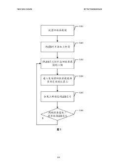
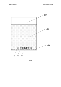
Method for recycling micro-element and recycling system therefor
PatentWO2021232450A1
Innovation
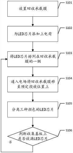
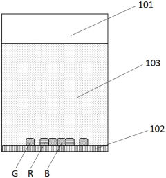
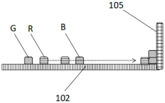
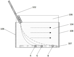
- By applying the first and second forces, the micro-elements that failed to be transferred are moved from the initial position to the target position, and the direction and intensity of the different forces are used to achieve the separation of different types of micro-elements, including the use of electric or magnetic fields to separate the charged micro-elements. The microcomponents move horizontally in a preset electric or magnetic field and fall into the collection device by gravity.
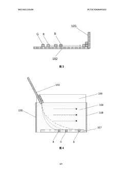
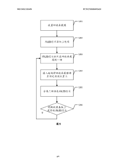
Micro-component recovery method and recovery system thereof
PatentActiveCN113707768A
Innovation
- By applying forces in different directions, the micro components are displaced from the initial position to the target position, and the electric field or magnetic field force is used to move horizontally. Separation and collection are achieved according to the different chip qualities. The recycling carrier film and collection device are used to separate and collect the micro components. Recycle.
Environmental Impact Assessment of MicroLED Manufacturing
The manufacturing processes of MicroLED displays involve numerous materials and chemicals that pose significant environmental concerns. Current production methods utilize rare earth elements, heavy metals, and various semiconductor materials that have substantial ecological footprints. The extraction of gallium, indium, and other critical elements for MicroLED fabrication contributes to habitat destruction, water pollution, and greenhouse gas emissions in mining regions.
Energy consumption represents another major environmental challenge. MicroLED manufacturing requires ultra-clean room environments, precise temperature control, and energy-intensive processes like metal-organic chemical vapor deposition (MOCVD) and photolithography. Studies indicate that the energy requirements for MicroLED production currently exceed those of conventional LED and LCD manufacturing by 30-45%, primarily due to the precision requirements and lower yields.
Water usage in MicroLED fabrication is particularly concerning, with estimates suggesting that producing a single 6-inch MicroLED wafer requires between 2,000-4,000 gallons of ultra-pure water. The resulting wastewater contains various contaminants including acids, solvents, and metal particulates that require extensive treatment before discharge.
Chemical waste management presents additional challenges. The etching processes utilize hydrofluoric acid, phosphoric acid, and other hazardous chemicals that require specialized handling and disposal protocols. Current industry practices vary significantly in effectiveness, with only approximately 60% of facilities implementing advanced chemical recovery systems.
Carbon emissions associated with MicroLED manufacturing stem from both direct energy consumption and the production of precursor materials. Life cycle assessments indicate that the carbon footprint of MicroLED displays currently exceeds that of OLED alternatives by approximately 15-20% when measured on a per-display-area basis, though this gap is narrowing with technological improvements.
Particulate emissions from manufacturing facilities also pose localized environmental and health concerns. The fine particulate matter generated during various fabrication steps can contribute to air quality degradation in surrounding communities if not properly filtered and controlled.
Despite these challenges, emerging manufacturing techniques show promise for reducing environmental impacts. Advanced recycling methods for process chemicals, closed-loop water systems, and more energy-efficient equipment are gradually being adopted by industry leaders, potentially reducing the ecological footprint of MicroLED production by 25-30% over the next five years according to industry projections.
Circular Economy Strategies for MicroLED Supply Chain
The circular economy approach to MicroLED manufacturing represents a paradigm shift from traditional linear production models toward sustainable, closed-loop systems. This strategy encompasses the entire supply chain, from raw material sourcing to end-of-life management, with the goal of minimizing waste and maximizing resource efficiency.
Material input optimization forms the foundation of circular economy strategies in the MicroLED supply chain. By designing components with recycling in mind, manufacturers can facilitate easier disassembly and material recovery. Advanced manufacturing techniques that reduce material waste during production, such as precision deposition methods and optimized lithography processes, contribute significantly to resource conservation.
Supplier engagement represents another critical aspect of circular economy implementation. Leading MicroLED manufacturers are establishing sustainability requirements for their suppliers, creating a ripple effect throughout the value chain. Collaborative initiatives between display manufacturers, material suppliers, and recycling facilities enable the development of standardized recovery protocols and technologies specifically tailored to MicroLED components.
Remanufacturing and refurbishment programs extend the useful life of MicroLED displays and components. These programs involve the collection, disassembly, inspection, and restoration of used products to functional condition, often with performance guarantees comparable to new products. The economic viability of such programs increases as MicroLED technology matures and becomes more widespread in consumer electronics.
Innovative business models are emerging to support circular economy principles in the MicroLED industry. Product-as-a-service offerings, where manufacturers retain ownership of physical products while customers pay for the service they provide, create incentives for producers to design for longevity and recyclability. These models align economic interests with environmental sustainability goals.
Technological innovations in recycling are particularly important for MicroLED sustainability. Advanced separation techniques using automated optical sorting, chemical processes, and mechanical methods enable the recovery of high-value materials like gallium nitride, indium, and rare earth elements from end-of-life displays. These recovered materials can then be reintroduced into the manufacturing process, reducing dependence on virgin resource extraction.
Policy frameworks and industry standards play a crucial role in accelerating circular economy adoption. Extended Producer Responsibility regulations, material passports that track component composition, and eco-design requirements create the necessary infrastructure for effective material cycling. Industry consortia are working to establish common standards for MicroLED recyclability and material recovery benchmarks.
Unlock deeper insights with Patsnap Eureka Quick Research — get a full tech report to explore trends and direct your research. Try now!
Generate Your Research Report Instantly with AI Agent
Supercharge your innovation with Patsnap Eureka AI Agent Platform!