Large Area Displays AR VR and Automotive Applications as MicroLED Case Studies
AUG 25, 20259 MIN READ
Generate Your Research Report Instantly with AI Agent
Patsnap Eureka helps you evaluate technical feasibility & market potential.
MicroLED Technology Background and Objectives
MicroLED technology represents a revolutionary advancement in display technology, emerging as a promising alternative to traditional LCD and OLED displays. Since its conceptual introduction in the early 2000s, MicroLED has evolved from laboratory experiments to commercial prototypes, with significant acceleration in development occurring over the past decade. The technology is characterized by arrays of microscopic LED elements that serve as individual pixel elements, typically measuring less than 100 micrometers.
The evolution of MicroLED technology has been marked by progressive miniaturization of LED chips, improvements in mass transfer techniques, and enhanced manufacturing processes. Initially limited by production challenges and high costs, recent breakthroughs in epitaxial growth techniques and pick-and-place technologies have significantly improved the commercial viability of MicroLED displays.
Current technological trends indicate a convergence toward more efficient manufacturing methods, including advances in wafer-level processing and innovative mass transfer techniques that enable the precise placement of millions of tiny LED elements. Additionally, there is a growing focus on improving the quantum efficiency of MicroLED emitters across different color spectrums, particularly in achieving balanced performance between red, green, and blue elements.
The primary technical objectives for MicroLED development center around addressing several key challenges. First, achieving cost-effective mass production capabilities that can compete with established display technologies. Second, developing reliable and scalable mass transfer processes that maintain high yield rates across large areas. Third, improving energy efficiency while maintaining superior brightness and contrast ratios that exceed current display technologies.
For large area displays, the objectives include developing seamless tiling solutions and addressing uniformity issues across expansive surfaces. In the AR/VR domain, the focus is on creating ultra-high pixel density displays with minimal power consumption and form factors suitable for wearable devices. For automotive applications, the goals include developing displays with extreme durability, wide operating temperature ranges, and exceptional visibility under varying lighting conditions.
The long-term vision for MicroLED technology encompasses achieving perfect black levels, wide color gamut coverage exceeding 120% of DCI-P3, brightness levels above 5,000 nits, and response times in microseconds rather than milliseconds. Additionally, there are aspirations to develop flexible and transparent MicroLED displays that can conform to various surfaces and integrate seamlessly with emerging form factors.
As the technology matures, the ultimate objective is to establish MicroLED as the dominant display technology across multiple sectors, offering unprecedented visual performance while achieving manufacturing economics that enable mass-market adoption across consumer electronics, professional displays, automotive interfaces, and next-generation augmented and virtual reality systems.
Market Analysis for MicroLED Displays
The global MicroLED display market is experiencing robust growth, projected to reach $21.1 billion by 2027, with a compound annual growth rate (CAGR) of 89.3% from 2021 to 2027. This exceptional growth trajectory is driven by several key factors, including increasing demand for brighter, more energy-efficient displays with superior color accuracy and contrast ratios across multiple application domains.
Large area displays represent a significant market segment, with MicroLED technology poised to disrupt the premium television and digital signage sectors. Samsung's The Wall and Sony's Crystal LED display systems have already demonstrated commercial viability in this space, though high production costs currently limit mass-market adoption. Industry analysts predict price points will decrease by approximately 60% over the next five years as manufacturing processes mature.
The AR/VR segment presents perhaps the most promising growth opportunity, with MicroLED displays addressing critical pain points in current headset designs. The technology's ability to deliver high brightness (exceeding 100,000 nits), ultra-low latency, and exceptional pixel density makes it ideal for near-eye display applications. Market research indicates that AR/VR device shipments incorporating MicroLED technology will grow at a CAGR of 124% through 2026.
Automotive applications constitute another rapidly expanding market segment, with MicroLED displays increasingly featured in heads-up displays (HUDs), digital dashboards, and center console displays. The automotive MicroLED market is expected to grow at a CAGR of 74.2% through 2027, driven by premium vehicle integration and the expanding autonomous vehicle sector requiring high-reliability display systems.
Regional analysis reveals Asia-Pacific as the dominant manufacturing hub, with Taiwan, South Korea, and China leading production capacity development. North America and Europe represent the largest initial markets for premium MicroLED products, though rapid adoption is anticipated across all regions as costs decrease.
Consumer electronics giants including Apple, Samsung, and LG Display have made substantial investments in MicroLED technology, with Apple alone filing over 50 MicroLED-related patents since 2018. Supply chain analysis indicates that mass production capabilities are developing rapidly, with key bottlenecks in mass transfer processes and yield rates gradually being resolved through innovative engineering approaches.
Market penetration is expected to follow a tiered approach, beginning with premium large-format displays and specialized AR/VR applications, followed by automotive integration, and eventually reaching mainstream consumer electronics as economies of scale reduce production costs to competitive levels against established OLED and mini-LED technologies.
Technical Challenges and Global Development Status
MicroLED technology faces significant technical challenges despite its promising potential for large area displays, AR/VR, and automotive applications. Mass transfer remains the foremost obstacle, as manufacturers struggle to efficiently place millions of microscopic LED chips with precise positioning and high yield rates. Current pick-and-place methods become increasingly inefficient as display resolution increases, creating a bottleneck in production scaling.
Defect management presents another critical challenge, as even minor defects can compromise display quality. The industry still lacks cost-effective inspection and repair processes for high-volume production, particularly for displays requiring millions of perfect pixels. This challenge is especially pronounced in AR/VR applications where pixel density requirements are extreme.
Color conversion and uniformity issues persist across the industry. Traditional approaches using phosphor conversion or RGB chips face efficiency trade-offs, with maintaining consistent brightness and color across large displays proving particularly difficult. Additionally, the driving circuits for MicroLED displays require sophisticated integration solutions that balance performance with manufacturing complexity.
Globally, MicroLED development shows distinct regional characteristics. North America leads in fundamental research and intellectual property, with companies like Apple making significant acquisitions and investments. Asia, particularly Taiwan, South Korea, and China, dominates in manufacturing infrastructure and supply chain development, with companies like Samsung, LG, and BOE advancing commercial production capabilities.
European entities focus on specialized applications and materials science innovations, particularly for automotive displays where stringent reliability requirements exist. Research institutions across Europe collaborate closely with automotive manufacturers to develop MicroLED solutions tailored to in-vehicle environments.
The development timeline reveals accelerating progress, with early research phase (2000-2015) giving way to rapid commercialization efforts since 2016. Recent years have seen significant breakthroughs in mass transfer techniques and manufacturing processes, though full commercial viability for consumer markets remains elusive.
Investment in MicroLED technology has surged globally, with estimated R&D spending exceeding $4.5 billion in 2022 alone. This reflects growing confidence in the technology's potential to disrupt multiple display markets. However, the technology readiness level varies significantly by application, with large-format displays approaching commercial viability while AR/VR implementations require further fundamental breakthroughs.
Standardization efforts remain fragmented, with multiple competing approaches to key manufacturing processes and materials. This lack of industry consensus potentially slows broader adoption and increases development costs across the ecosystem.
Current MicroLED Implementation Solutions
01 MicroLED fabrication and transfer techniques
Various methods for fabricating and transferring microLED devices from a source substrate to a target substrate. These techniques include mass transfer processes, selective transfer methods, and pick-and-place approaches that enable efficient production of microLED displays. The processes often involve temporary bonding layers, release mechanisms, and precision alignment systems to ensure accurate placement of the microLED elements.- MicroLED fabrication and transfer techniques: Various methods for fabricating and transferring microLED devices from a source substrate to a target substrate. These techniques include mass transfer processes, selective transfer methods, and pick-and-place approaches that enable efficient handling of microscale LED elements. The processes often involve temporary adhesive layers, carrier substrates, and precision alignment systems to ensure accurate positioning of the microLED elements on display panels.
- MicroLED display panel structures: Structural designs and configurations of microLED display panels, including pixel arrangements, substrate materials, and integration with driving circuits. These structures often incorporate thin-film transistor (TFT) backplanes, specialized electrode configurations, and optical enhancement layers to improve display performance. The designs focus on achieving high resolution, brightness uniformity, and color accuracy while maintaining thin form factors.
- MicroLED thermal management solutions: Thermal management approaches for microLED displays to address heat dissipation challenges. These solutions include specialized heat sink designs, thermally conductive materials, and structural configurations that facilitate efficient heat transfer away from the LED elements. Effective thermal management is crucial for maintaining device performance, reliability, and longevity, particularly in high-brightness applications.
- MicroLED driving and control systems: Electronic driving and control systems specifically designed for microLED displays. These systems include specialized integrated circuits, pulse width modulation techniques, and current control mechanisms to achieve precise brightness control and color reproduction. The driving architectures are optimized to handle the unique electrical characteristics of microLEDs while minimizing power consumption and ensuring uniform light output across the display.
- MicroLED semiconductor material innovations: Advancements in semiconductor materials used in microLED fabrication, including novel epitaxial structures, quantum well designs, and doping profiles. These innovations focus on improving the internal quantum efficiency, light extraction, and wavelength stability of microLEDs. Material developments also address challenges related to efficiency droop, color shift, and device degradation, particularly for blue and green microLED elements.
02 MicroLED display structures and configurations
Structural designs and configurations of microLED displays, including pixel arrangements, substrate layouts, and integration with driving circuits. These structures may incorporate various layers for improved light emission, electrical connectivity, and mechanical stability. The configurations often address challenges related to pixel density, color reproduction, and form factor requirements for different display applications.Expand Specific Solutions03 Thermal management in microLED devices
Solutions for managing heat generation and dissipation in microLED displays. These approaches include specialized heat sink designs, thermal interface materials, and cooling structures integrated into the display assembly. Effective thermal management is crucial for maintaining device performance, reliability, and longevity, especially in high-brightness applications where microLEDs generate significant heat.Expand Specific Solutions04 MicroLED driving and control systems
Circuit designs and control systems for driving microLED displays, including backplane technologies, addressing schemes, and power management solutions. These systems enable precise control of individual microLED elements for accurate brightness and color reproduction. Advanced driving architectures may incorporate compensation mechanisms for device variations and aging effects to maintain uniform display performance over time.Expand Specific Solutions05 MicroLED manufacturing processes and equipment
Specialized equipment and manufacturing processes developed specifically for microLED production, including epitaxial growth systems, lithography tools, and inspection equipment. These manufacturing solutions address challenges in mass production such as yield improvement, defect detection, and process automation. Advanced manufacturing techniques enable cost-effective production of microLED displays at commercial scale with consistent quality.Expand Specific Solutions
Key Industry Players and Ecosystem
MicroLED technology for large area displays, AR/VR, and automotive applications is currently in the early commercialization phase, with the market expected to grow significantly from approximately $2.7 billion in 2021 to over $10 billion by 2026. The competitive landscape features established display manufacturers like Samsung, LG Display, and BOE Technology alongside specialized MicroLED innovators such as VerLASE Technologies and Jade Bird Display. Major tech companies including Apple, Meta, and Google are investing heavily in MicroLED for AR/VR applications, while automotive players are exploring MicroLED for next-generation dashboards and lighting. Technical challenges in mass transfer, yield improvement, and cost reduction remain, though companies like Lumileds, OSRAM, and Kubos Semiconductors are making significant advances in addressing these barriers through innovative manufacturing processes and materials science breakthroughs.
BOE Technology Group Co., Ltd.
Technical Solution: BOE has developed an innovative MicroLED display technology platform utilizing chip-scale packaging and advanced mass transfer processes. Their approach features direct RGB emission MicroLEDs with sizes ranging from 30μm to 50μm, achieving pixel densities up to 2000 PPI for AR/VR applications. BOE's manufacturing process employs a proprietary fluidic assembly technique for large-area displays, allowing for efficient placement of millions of MicroLEDs simultaneously. For automotive applications, they've created high-brightness (>5000 nits) MicroLED displays with operating temperature ranges from -40°C to 105°C, meeting stringent automotive reliability standards. Their technology incorporates specialized thin-film encapsulation to protect MicroLEDs from environmental factors while maintaining optical performance. Recent innovations include development of a hybrid OLED-MicroLED architecture that combines the benefits of both technologies, and advancements in red MicroLED efficiency through quantum dot conversion layers.
Strengths: Large-scale manufacturing infrastructure allowing for rapid scaling of production; strong position in the Chinese domestic market providing significant capital for R&D; vertical integration from LED chip production to final display assembly. Weaknesses: Less established presence in premium automotive and AR/VR markets compared to competitors; challenges in achieving uniform color performance across very large displays; relatively newer entrant to MicroLED-specific technology development.
Meta Platforms Technologies LLC
Technical Solution: Meta has developed specialized MicroLED technology primarily focused on AR/VR applications, featuring ultra-high pixel density displays exceeding 5000 PPI with minimal screen door effect. Their approach utilizes monolithically integrated MicroLEDs on silicon backplanes, enabling extremely compact form factors essential for lightweight AR glasses. Meta's manufacturing process incorporates a proprietary wafer-level integration technique that allows for precise placement of RGB MicroLEDs at the micrometer scale. Their technology achieves brightness levels up to 20,000 nits while maintaining power efficiency below 5W for full-display operation, critical for battery-powered wearable devices. Meta has pioneered advanced optical waveguide integration with MicroLED displays, creating holographic and light field capabilities for enhanced AR experiences. Recent innovations include development of eye-tracking optimized variable resolution displays that concentrate pixel density where users are looking, and specialized color management systems that compensate for the unique optical characteristics of near-eye MicroLED implementations.
Strengths: Extensive research in human visual perception allowing for optimized MicroLED displays for AR/VR; significant financial resources dedicated to advanced display research; strong integration capabilities between display hardware and software systems. Weaknesses: Less experience in large-area display manufacturing compared to traditional display companies; limited presence in automotive applications; higher dependency on external suppliers for certain MicroLED components.
Core Patents and Technical Innovations
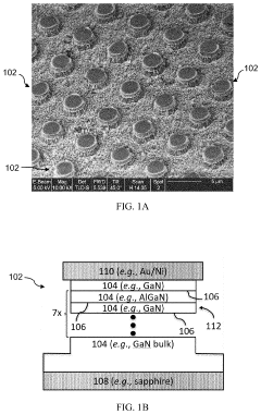
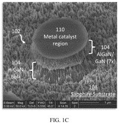
Light emitting diode (LED) structures for a microled device, and method for producing an array of LED structures
PatentPendingUS20230317871A1
Innovation
- The use of metal-assisted chemical etching to form heterostructure micropillars with semiconductor layers separated by heterojunctions, where the etching process is conducted using a solution or vapor with optional above-gap radiation, avoiding ion-induced defects by forming the micropillars with metal catalyst regions that can be removed post-processing.
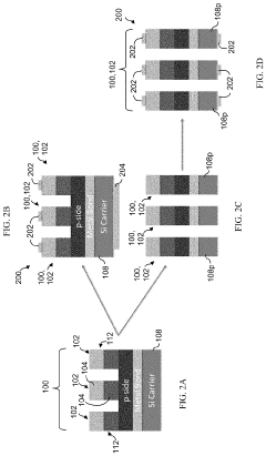
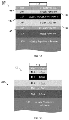
Semiconductor device comprising microled structures
PatentPendingEP4564435A1
Innovation
- The proposed solution involves growing microLED structures on InGaN platelets monolithically grown on an epiwafer, using an upper mask layer with apertures that are smaller than the top c-plane surface, allowing for precise control of microLED growth and emission wavelength.
Manufacturing Scalability and Cost Reduction Strategies
The manufacturing scalability of MicroLED technology represents one of the most significant challenges in its widespread adoption across large area displays, AR/VR devices, and automotive applications. Current manufacturing processes face substantial yield issues, particularly in the mass transfer process where millions of microscopic LED chips must be precisely positioned. Industry data indicates yield rates below 70% for high-resolution displays, significantly impacting production costs.
Several promising strategies are emerging to address these manufacturing challenges. Parallel transfer techniques, which can simultaneously position thousands of MicroLED chips, have demonstrated up to 5x improvement in production throughput compared to serial transfer methods. Companies like X-Celeprint and eLux have developed innovative approaches using elastomer stamps and fluidic assembly, respectively, showing potential for scaling to industrial production levels.
Cost reduction initiatives are focusing on substrate material optimization, with significant research directed toward silicon and glass substrates as alternatives to traditional sapphire. Silicon substrates could potentially reduce material costs by 30-40% while offering better integration with driving circuits. Additionally, equipment manufacturers are developing specialized tools for MicroLED production that combine higher precision with increased throughput.
Vertical integration of the supply chain represents another critical strategy, with major display manufacturers acquiring specialized MicroLED startups to consolidate intellectual property and manufacturing expertise. This integration has shown potential to reduce production costs by eliminating markup between supply chain segments and optimizing processes across the manufacturing pipeline.
Automation and AI-driven quality control systems are being implemented to address defect detection and repair processes. Advanced machine vision systems can now identify defective pixels at rates exceeding 99.9% accuracy, while automated repair mechanisms can replace or bypass faulty MicroLEDs, significantly improving final yield rates and reducing labor costs.
Standardization efforts across the industry are beginning to emerge, with consortiums working to establish common specifications for MicroLED components. These initiatives could potentially reduce development costs and accelerate manufacturing scalability by creating more unified supply chains and production methodologies.
Recent industry forecasts suggest that with continued implementation of these strategies, MicroLED manufacturing costs could decrease by 60-70% over the next five years, potentially bringing the technology to price parity with premium OLED displays for certain applications by 2027-2028, particularly in the automotive and AR/VR segments where the technology's advantages justify premium positioning.
Energy Efficiency and Environmental Impact
MicroLED technology represents a significant advancement in display technology with promising energy efficiency characteristics that position it as a sustainable alternative to conventional display technologies. When compared to traditional LCD displays, MicroLED consumes substantially less power due to its self-emissive nature, eliminating the need for backlighting systems that account for significant energy consumption in LCD panels.
The energy efficiency of MicroLED displays stems from their pixel-level light emission control, allowing precise illumination only where needed. This selective activation mechanism can reduce power consumption by up to 70% compared to conventional display technologies, particularly beneficial for large area displays where energy requirements scale with size. For AR/VR applications, this efficiency translates to extended battery life in portable devices, addressing one of the most significant limitations in current immersive technology adoption.
In automotive applications, MicroLED's energy efficiency contributes to extended range in electric vehicles, where display systems represent an increasingly significant portion of onboard power consumption. The technology's ability to maintain high brightness levels with lower power input makes it particularly suitable for automotive displays that must remain visible under varying lighting conditions while minimizing drain on vehicle electrical systems.
From an environmental perspective, MicroLED manufacturing processes currently present mixed implications. While the technology eliminates certain harmful materials found in competing technologies like mercury in LCDs, the production process involves specialized materials and precision manufacturing that can be resource-intensive. Industry analysis indicates that manufacturing energy requirements remain higher than established technologies, though economies of scale are expected to improve this aspect as production volumes increase.
The extended operational lifespan of MicroLED displays—estimated at 100,000+ hours compared to 30,000-50,000 hours for OLED—represents another environmental advantage through reduced electronic waste generation. This longevity is particularly valuable in automotive applications where displays are expected to match vehicle lifespans of 10+ years without degradation.
Carbon footprint assessments of complete lifecycle analyses show that despite higher initial manufacturing energy requirements, the operational efficiency of MicroLED technology results in net positive environmental impact for displays with moderate to heavy usage patterns. Recent industry initiatives focus on developing recycling protocols specifically for MicroLED components, addressing end-of-life considerations that will be crucial as the technology achieves mainstream adoption across large area displays, AR/VR devices, and automotive applications.
Unlock deeper insights with Patsnap Eureka Quick Research — get a full tech report to explore trends and direct your research. Try now!
Generate Your Research Report Instantly with AI Agent
Supercharge your innovation with Patsnap Eureka AI Agent Platform!