Wafer to Wafer versus Die to Wafer Trade Offs in MicroLED Assembly
AUG 25, 20259 MIN READ
Generate Your Research Report Instantly with AI Agent
Patsnap Eureka helps you evaluate technical feasibility & market potential.
MicroLED Assembly Background and Objectives
MicroLED technology has emerged as a promising next-generation display technology, offering superior brightness, energy efficiency, contrast ratio, and color gamut compared to traditional LCD and OLED displays. The evolution of MicroLED technology began in the early 2000s, with significant advancements occurring over the past decade as manufacturers sought alternatives to existing display technologies that could overcome inherent limitations in brightness and longevity.
The assembly process represents one of the most critical challenges in MicroLED commercialization. Two primary approaches have emerged: Wafer-to-Wafer (W2W) and Die-to-Wafer (D2W) assembly methods. Each approach presents distinct advantages and limitations that significantly impact manufacturing efficiency, yield rates, and ultimate product performance.
The W2W approach involves transferring entire arrays of MicroLEDs from a source wafer to a target wafer simultaneously. This method emerged from traditional semiconductor manufacturing techniques and offers potential advantages in throughput for mass production scenarios. Conversely, the D2W approach involves picking and placing individual MicroLED dies onto a target substrate, offering greater flexibility but potentially lower throughput.
The technical evolution trajectory shows a clear trend toward improving transfer efficiency, yield rates, and placement accuracy. Early MicroLED assembly techniques suffered from low yields and damage during transfer, but recent innovations have dramatically improved these metrics. The industry has witnessed a progression from rudimentary stamp-based transfer methods to sophisticated equipment utilizing electrostatic, laser-assisted, and fluidic self-assembly techniques.
The primary objective of this technical research is to comprehensively evaluate the trade-offs between W2W and D2W assembly approaches for MicroLED manufacturing. Specifically, we aim to analyze factors including throughput capabilities, defect management strategies, placement accuracy, scalability to different display sizes, and overall cost implications across various production volumes.
Additionally, this research seeks to identify potential hybrid approaches that might combine advantages from both methods, as well as emerging technologies that could fundamentally alter the current manufacturing paradigms. Understanding these trade-offs is crucial for strategic decision-making regarding manufacturing investments and technology development roadmaps.
The findings from this analysis will inform future R&D directions and help establish optimal manufacturing strategies for different MicroLED applications, ranging from small wearable displays to large-format televisions and specialized high-brightness displays for automotive and AR/VR applications.
Market Analysis for MicroLED Display Technologies
The MicroLED display market is experiencing significant growth, driven by increasing demand for high-performance displays across various applications. Current market projections indicate that the global MicroLED display market is expected to reach $19.8 billion by 2026, growing at a CAGR of 89.3% from 2021. This exponential growth reflects the technology's potential to disrupt traditional display markets dominated by LCD and OLED technologies.
Consumer electronics represents the largest application segment, with smartphones, smartwatches, and AR/VR headsets leading adoption. The automotive sector follows closely, where MicroLED displays offer advantages in brightness, durability, and energy efficiency for dashboard displays and infotainment systems. Television manufacturers are also investing heavily in MicroLED technology, particularly for premium large-format displays where its superior contrast ratio and color gamut provide competitive advantages.
Regional analysis shows Asia-Pacific dominating the MicroLED manufacturing landscape, with South Korea, Taiwan, and China leading in production capacity. North America and Europe focus primarily on research and development of advanced assembly techniques, including both Wafer-to-Wafer (W2W) and Die-to-Wafer (D2W) approaches.
Market segmentation by assembly method reveals interesting trends. W2W assembly currently accounts for approximately 35% of the market, primarily in applications requiring smaller displays with extremely high pixel density. D2W assembly represents about 65% of the market, favored for its flexibility in display size and better defect management capabilities.
Consumer demand is increasingly driven by performance metrics where MicroLED excels: brightness (up to 5,000 nits), contrast ratio (1,000,000:1), response time (under 1 microsecond), and energy efficiency (30-50% more efficient than OLED). These performance advantages are creating premium market segments where consumers are willing to pay significant price premiums.
Supply chain analysis reveals that mass production challenges remain the primary market constraint. The choice between W2W and D2W assembly methods significantly impacts production costs, yield rates, and scalability. Current production costs for MicroLED displays remain 5-8 times higher than equivalent OLED displays, primarily due to assembly complexities and yield issues.
Market forecasts indicate that as assembly technologies mature, particularly with improvements in D2W processes, production costs could decrease by 60-70% over the next five years. This cost reduction trajectory will likely trigger mass market adoption, particularly in mid-range consumer electronics and automotive applications where the technology's durability and performance advantages justify the premium.
Current Challenges in MicroLED Mass Transfer
MicroLED mass transfer represents one of the most critical bottlenecks in the commercialization pathway for MicroLED displays. The industry currently faces significant challenges in efficiently transferring millions of tiny LED chips from their growth substrate to the display backplane. Two dominant approaches have emerged: Wafer-to-Wafer (W2W) and Die-to-Wafer (D2W) transfer methods, each presenting distinct advantages and limitations.
The W2W approach involves transferring entire arrays of microLEDs simultaneously from the donor wafer to the receiving substrate. While this method offers higher throughput potential, it struggles with yield issues. When transferring complete arrays, any defective microLEDs in the donor wafer are also transferred, requiring subsequent repair processes. Additionally, W2W transfer demands precise alignment between differently sized wafers and struggles with thermal expansion coefficient mismatches between the donor and receiving substrates.
Conversely, D2W methods involve selecting and transferring individual dies or small groups of dies. This approach enables known-good-die selection, significantly improving final yield. However, D2W methods typically demonstrate lower throughput compared to W2W approaches, as individual or small batches of microLEDs must be picked and placed sequentially. This creates a fundamental trade-off between transfer speed and final display quality.
Both approaches face common challenges in handling extremely small microLED chips (typically <50μm) without causing damage. The delicate nature of these miniature components requires sophisticated pick-and-place tools with micron-level precision. Surface contamination and electrostatic discharge during transfer pose additional risks to device performance and reliability.
Mass transfer equipment manufacturers are actively developing hybrid approaches that attempt to combine the throughput advantages of W2W with the selective capabilities of D2W. These include selective stamp transfer methods and massively parallel pick-and-place systems utilizing microfluidic or electromagnetic manipulation techniques.
Another significant challenge lies in achieving consistent electrical and optical performance across transferred microLEDs. Variations in transfer pressure, adhesive properties, or thermal conditions during bonding can lead to inconsistent performance characteristics across the display, resulting in visible non-uniformities to end users.
The economic viability of mass transfer solutions remains problematic. Current equipment costs and processing times make microLED displays prohibitively expensive for most consumer applications. Industry estimates suggest that transfer costs need to decrease by an order of magnitude to enable widespread adoption in mainstream display products beyond premium segments.
W2W vs D2W Technical Implementation Approaches
01 Mass transfer techniques for microLED assembly
Various mass transfer techniques are employed for microLED assembly, including pick-and-place methods, fluidic assembly, and electrostatic transfer. These techniques enable the efficient transfer of large quantities of microLED chips from a donor substrate to a target substrate. The choice of transfer method impacts manufacturing throughput, placement accuracy, and yield rates. Advanced mass transfer techniques can significantly reduce assembly time while maintaining precise positioning of microLED elements.- Mass transfer techniques for MicroLED assembly: Various mass transfer techniques are employed for efficient MicroLED assembly, including pick-and-place methods, fluidic assembly, and elastomeric stamp transfer. These techniques allow for the simultaneous transfer of multiple microLED chips from a donor substrate to a target substrate, significantly improving manufacturing throughput. The choice of transfer method impacts yield, alignment precision, and compatibility with different substrate materials, presenting important trade-offs in the assembly process.
- Bonding methods and interface considerations: Different bonding methods for microLED assembly include eutectic bonding, thermocompression bonding, and adhesive bonding. Each method presents trade-offs between bonding strength, electrical conductivity, thermal management, and process complexity. The interface between microLEDs and the substrate is critical for device performance, with considerations for thermal expansion coefficient matching, electrical connectivity, and mechanical stability affecting the long-term reliability of the assembled devices.
- Repair and redundancy strategies: Assembly methods incorporate repair and redundancy strategies to address yield challenges in microLED manufacturing. These include in-line testing and repair processes, redundant pixel architectures, and reworkable assembly techniques. The trade-offs involve increased manufacturing complexity versus improved final product yield, with considerations for cost, time efficiency, and equipment requirements. Effective repair strategies are essential for commercial viability of microLED displays, particularly for high-resolution applications.
- Alignment and precision control systems: Precision alignment systems are crucial for microLED assembly, utilizing advanced optical recognition, fiducial markers, and automated positioning systems. The trade-offs involve balancing positioning accuracy with assembly speed and equipment complexity. Sub-micron alignment precision is often required, particularly for high-resolution displays, necessitating sophisticated control systems. The choice of alignment method impacts yield, throughput, and capital equipment costs in the manufacturing process.
- Scalability and automation considerations: Scalability and automation are key considerations in microLED assembly method selection. Fully automated assembly lines offer high throughput but require significant capital investment, while semi-automated approaches provide flexibility at lower volumes. Trade-offs exist between initial equipment costs, production volume capabilities, and manufacturing flexibility. Assembly methods must balance precision requirements with production speed to achieve commercially viable manufacturing processes, particularly as display sizes increase and pixel densities improve.
02 Bonding technologies for microLED integration
Different bonding technologies are used to secure microLEDs to substrates, including eutectic bonding, thermocompression bonding, and adhesive bonding. Each bonding method presents trade-offs between bond strength, electrical conductivity, thermal performance, and processing temperature requirements. The selection of appropriate bonding technology affects device reliability, operational lifetime, and manufacturing complexity. Advanced bonding approaches may incorporate hybrid techniques to optimize both mechanical stability and electrical performance.Expand Specific Solutions03 Substrate preparation and compatibility considerations
Substrate preparation plays a crucial role in microLED assembly, with considerations for surface treatment, planarization, and electrode patterning. The choice of substrate material (glass, silicon, flexible polymers) presents trade-offs in terms of thermal expansion matching, optical properties, and cost. Compatibility between the microLED chips and substrate affects yield, reliability, and device performance. Advanced substrate engineering techniques can improve alignment accuracy and reduce stress-induced failures during the assembly process.Expand Specific Solutions04 Alignment and positioning systems for precision assembly
Precision alignment systems are essential for accurate microLED placement, utilizing machine vision, fiducial markers, and automated positioning equipment. Trade-offs exist between alignment accuracy, throughput speed, and system complexity. High-precision alignment technologies can achieve sub-micron placement accuracy but may require longer processing times. The selection of alignment methodology impacts manufacturing yield, pixel pitch capabilities, and display uniformity in the final microLED devices.Expand Specific Solutions05 Testing and repair strategies in microLED manufacturing
Testing and repair strategies are implemented throughout the microLED assembly process to identify and address defects. In-line testing methods include electrical probing, optical inspection, and functional testing of assembled arrays. Repair techniques such as redundant pixel design and selective replacement of defective microLEDs present trade-offs between manufacturing complexity, yield improvement, and cost. Advanced testing protocols can enhance overall production efficiency by identifying defects early in the assembly process.Expand Specific Solutions
Key Industry Players in MicroLED Manufacturing
The MicroLED assembly market is currently in its early growth phase, characterized by significant technological competition between Wafer-to-Wafer (W2W) and Die-to-Wafer (D2W) approaches. The global MicroLED market is projected to expand rapidly, with major players developing distinct technological advantages. Companies like Samsung, BOE Technology, and Meta Platforms are advancing W2W bonding for high-density displays, while Intel, Micron, and TSMC are focusing on D2W techniques offering greater flexibility. Qualcomm and Imec are developing hybrid approaches to balance yield and cost efficiency. The technology maturity varies significantly, with W2W showing higher throughput but limited substrate compatibility, while D2W offers better yield for heterogeneous integration despite slower processing speeds. This competitive landscape reflects the industry's search for optimal mass-production solutions.
Interuniversitair Micro-Electronica Centrum VZW
Technical Solution: IMEC has developed cutting-edge research solutions for MicroLED assembly that address fundamental challenges in both W2W and D2W approaches. Their W2W technology focuses on heterogeneous integration of III-V LED structures with CMOS backplanes through advanced direct bonding techniques. This process utilizes plasma-activated surface preparation and sub-200°C bonding temperatures to create robust interfaces while preserving the integrity of both the LED and CMOS structures. IMEC's research has demonstrated bonding strength exceeding 2 J/m² with alignment accuracy better than 0.5μm across 300mm wafers. For D2W applications, IMEC has pioneered a parallel transfer approach using laser-assisted release mechanisms that can selectively transfer microLEDs as small as 1μm with precise placement control. Their technology incorporates in-situ metrology that provides real-time feedback on transfer quality and alignment accuracy. IMEC has also developed innovative repair strategies for both approaches, including localized laser repair for W2W defects and selective replacement techniques for D2W processes. Their research demonstrates pathways to achieving transfer yields above 99.999% through combined process optimization and repair strategies.
Strengths: World-class research capabilities with access to advanced process equipment; excellent understanding of fundamental material interfaces; innovative approaches to yield improvement. Weaknesses: Technologies still primarily in research phase rather than high-volume manufacturing; higher costs associated with precision equipment; challenges with scaling to commercial production volumes.
Samsung Electronics Co., Ltd.
Technical Solution: Samsung has pioneered a comprehensive approach to MicroLED assembly, developing both W2W and D2W technologies with distinct applications. Their W2W solution employs a proprietary low-temperature fusion bonding technique that creates direct semiconductor-to-semiconductor interfaces without intermediate adhesives, resulting in superior electrical and thermal performance. This process operates at temperatures below 300°C to prevent damage to the quantum well structures in the LED epitaxial layers. For their commercial display products, Samsung has implemented a sophisticated D2W process using elastomeric stamp transfer technology that can selectively pick and place thousands of microLEDs in a single operation. Their system incorporates machine vision alignment with sub-micron accuracy and real-time placement verification. Samsung's latest generation transfer equipment can handle dies as small as 3μm with pitch accuracy of ±0.5μm. The company has also developed repair strategies for both approaches, with automated detection and replacement systems that can identify and correct defective pixels post-transfer.
Strengths: Highly mature manufacturing processes with proven commercial implementation; excellent thermal management in W2W approach; superior flexibility in pixel distribution with D2W method. Weaknesses: D2W approach faces throughput limitations for very high-resolution displays; repair processes add manufacturing complexity and cost; challenges with ultra-small pixel handling.
Critical Patents and Innovations in Transfer Technologies
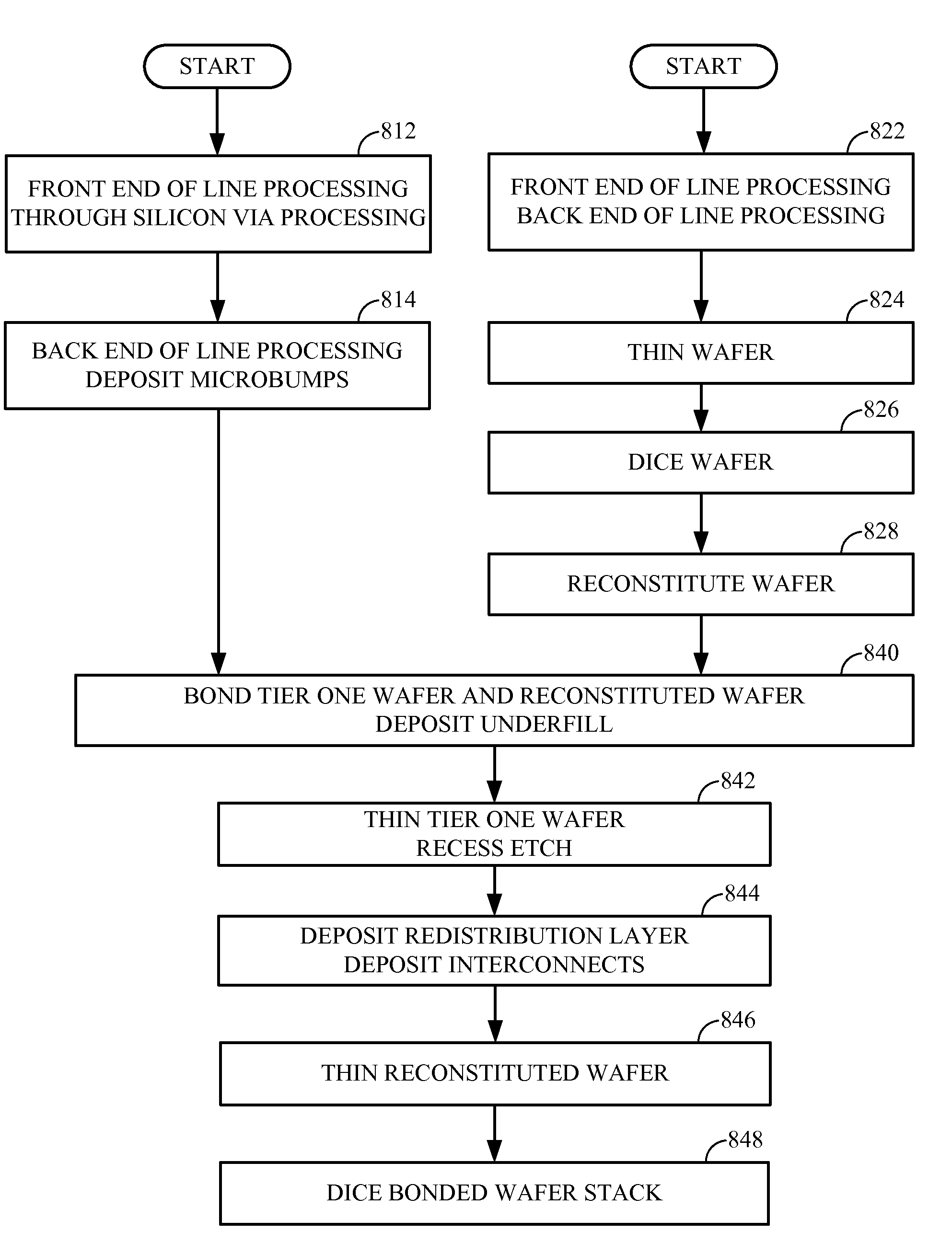
Low cost die-to-wafer alignment/bond for 3D IC stacking
PatentWO2010036579A2
Innovation
- The method involves orienting multiple die with an axis of symmetry for each tier, allowing for simultaneous alignment and bonding, reducing the number of alignment processes and enabling multiple die to be bonded in a single step, thereby increasing throughput and yield.
Semiconductor Wafer-To-Wafer Bonding For Dissimilar Semiconductor Dies And/Or Wafers
PatentActiveUS20110049694A1
Innovation
- The method involves aligning and bonding a reconstituted wafer with a first wafer, where the second die's interconnect structure on the reconstituted wafer aligns with the first die's interconnect on the first wafer, allowing for the creation of a stacked wafer with dissimilar die sizes using wafer-to-wafer bonding, which reduces the need for carrier wafers and enhances manufacturing efficiency.
Cost-Benefit Analysis of Assembly Methods
The economic analysis of MicroLED assembly methods reveals significant cost differentials between Wafer-to-Wafer (W2W) and Die-to-Wafer (D2W) approaches. W2W bonding typically offers lower per-unit costs at high volumes due to parallel processing capabilities, handling entire wafers simultaneously rather than individual dies. This efficiency translates to approximately 15-20% lower manufacturing costs when operating at full capacity with high yield rates.
However, the cost advantage of W2W diminishes considerably when yield factors are introduced. Since W2W bonding requires both the display backplane and the LED wafer to have matching yields, defects in either component affect the entire assembly. Industry data suggests that with current technology, W2W processes may waste 30-40% of good LEDs when paired with lower-yield backplanes, significantly increasing the effective cost per functional display.
D2W assembly, while initially more expensive due to the need for precise pick-and-place equipment and longer processing times, demonstrates superior cost-effectiveness when working with non-uniform materials or varying quality components. The ability to selectively place only known-good dies (KGD) results in material savings that can offset the higher equipment and process costs, particularly for larger display sizes where yield becomes increasingly critical.
Capital expenditure requirements also differ substantially between the two approaches. W2W bonding equipment typically requires 30-50% higher initial investment but offers greater throughput potential. D2W systems, while less expensive initially, often incur higher operational costs due to maintenance requirements for the precision placement mechanisms and longer cycle times.
Energy consumption analysis indicates that W2W processes generally consume 25-35% less energy per unit produced at scale, contributing to lower operational expenses in high-volume scenarios. This advantage stems from the batch processing nature of wafer-level handling versus the sequential operations required for individual die placement.
Labor costs favor W2W for high-volume production, requiring approximately 40% fewer operator hours per unit. However, D2W offers greater flexibility for specialized or lower-volume applications, allowing manufacturers to balance capital investment against production needs more effectively.
The break-even analysis suggests that W2W becomes economically advantageous when production volumes exceed 10,000-15,000 wafers annually and combined yield rates surpass 85%. Below these thresholds, D2W typically provides better return on investment and lower risk, particularly for emerging applications or specialized display configurations.
Supply Chain Considerations for MicroLED Production
The MicroLED supply chain presents unique challenges compared to traditional display technologies, requiring specialized equipment, materials, and expertise. When considering Wafer-to-Wafer (W2W) versus Die-to-Wafer (D2W) assembly approaches, supply chain implications become particularly significant.
W2W assembly necessitates a more vertically integrated supply chain structure, as it requires tight coordination between wafer fabrication facilities and assembly operations. This approach typically demands fewer suppliers but places greater emphasis on those suppliers' capabilities to deliver consistently high-quality wafers with minimal defects. The supply chain for W2W tends to be less geographically distributed, often concentrating manufacturing operations in technology hubs with established semiconductor infrastructure.
In contrast, D2W assembly enables a more distributed supply chain model. Individual dies can be sourced from multiple suppliers and locations, allowing for greater flexibility in procurement strategies. This approach facilitates a more modular supply chain where specialized vendors can focus on specific components or processes, potentially reducing dependency on single suppliers.
Material flow considerations differ significantly between these approaches. W2W requires synchronized delivery of complete wafers, creating potential bottlenecks if any supplier experiences delays. D2W allows for more granular inventory management, with dies being stored and transported more easily than full wafers, though requiring more sophisticated tracking systems to manage the increased number of individual components.
Quality control checkpoints must be strategically positioned throughout both supply chains, but with different emphases. W2W requires intensive pre-bonding inspection of entire wafers, while D2W enables more distributed quality control with opportunities to select only known-good dies, potentially reducing waste but increasing handling complexity.
Equipment suppliers face different challenges depending on the assembly method. W2W requires precision alignment tools capable of handling full wafers with minimal distortion, while D2W necessitates high-speed pick-and-place equipment with advanced vision systems for individual die handling. This divergence creates specialized niches within the equipment supply sector.
Regional considerations also impact supply chain design. Regions with established semiconductor infrastructure may favor W2W approaches, while emerging manufacturing hubs might find D2W's lower initial capital requirements more accessible. Regulatory environments regarding technology transfer and export controls can further influence supply chain geography, particularly for advanced MicroLED technologies with potential dual-use applications.
Unlock deeper insights with Patsnap Eureka Quick Research — get a full tech report to explore trends and direct your research. Try now!
Generate Your Research Report Instantly with AI Agent
Supercharge your innovation with Patsnap Eureka AI Agent Platform!