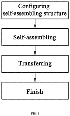
Electrostatic and Fluidic Approaches to MicroLED Mass Transfer
AUG 25, 20259 MIN READ
Generate Your Research Report Instantly with AI Agent
Patsnap Eureka helps you evaluate technical feasibility & market potential.
MicroLED Transfer Technology Background and Objectives
MicroLED technology has emerged as a revolutionary advancement in display technology, promising superior performance characteristics compared to traditional LCD and OLED displays. The evolution of this technology began in the early 2000s with the development of inorganic LED materials capable of emitting light at microscopic scales. Over the past decade, significant progress has been made in miniaturizing LEDs to dimensions below 50 micrometers, enabling high-resolution display applications.
The technical trajectory of MicroLED displays has been characterized by continuous improvements in pixel density, energy efficiency, and color reproduction. However, mass production has remained elusive due to manufacturing challenges, particularly in the transfer process of millions of tiny LED chips from growth substrates to display backplanes with precise positioning requirements.
Electrostatic and fluidic approaches represent two promising methodologies for addressing the mass transfer bottleneck in MicroLED production. Electrostatic transfer utilizes controlled electric fields to selectively pick and place MicroLED chips, while fluidic approaches leverage liquid medium dynamics to facilitate the movement and positioning of these microscopic components.
The primary technical objective in this domain is to develop scalable, high-throughput transfer processes capable of handling millions of MicroLED chips with sub-micron placement accuracy, minimal yield loss, and economically viable production costs. Current transfer technologies typically achieve throughput rates of thousands of units per hour, whereas commercial viability requires rates in the millions per hour while maintaining defect rates below 1 ppm.
Industry projections indicate that MicroLED displays could capture significant market share in premium display segments by 2025, with broader adoption contingent upon solving these manufacturing challenges. The global display industry has recognized this potential, with major investments in MicroLED technology exceeding $4 billion over the past five years.
The technical evolution trend points toward hybrid approaches that combine multiple transfer mechanisms, including electrostatic and fluidic principles, to overcome the limitations of individual methods. Recent advancements in microfluidic control systems and electrostatic field manipulation have demonstrated promising results in laboratory settings, achieving transfer yields above 99% for small-scale demonstrations.
As the technology continues to mature, we anticipate a convergence of complementary techniques that address different aspects of the transfer challenge, potentially enabling the first commercially viable mass production processes within the next 3-5 years. This would represent a significant milestone in display technology, potentially disrupting existing market dynamics and enabling entirely new product categories.
Market Analysis for MicroLED Display Applications
The MicroLED display market is experiencing significant growth, driven by the technology's superior performance characteristics compared to traditional display technologies. Current market projections indicate that the global MicroLED market is expected to reach $19.8 billion by 2026, with a compound annual growth rate of approximately 89.3% from 2021 to 2026. This explosive growth is fueled by increasing demand for brighter, more energy-efficient displays with higher resolution and contrast ratios.
Consumer electronics represents the largest application segment for MicroLED displays, with smartphones, smartwatches, and AR/VR headsets leading adoption. Apple's interest in the technology for future iPhone and Apple Watch models has been particularly notable, potentially serving as a catalyst for broader market acceptance. The automotive sector is emerging as another significant market, with luxury vehicle manufacturers incorporating MicroLED displays in dashboard and entertainment systems.
Market analysis reveals that mass transfer technology, particularly electrostatic and fluidic approaches, represents a critical bottleneck in the commercialization of MicroLED displays. The efficiency and cost-effectiveness of these transfer methods directly impact production yields and final product pricing. Currently, the high manufacturing costs associated with inefficient transfer methods are limiting mass market penetration, with MicroLED displays primarily targeting premium product segments.
Regional analysis shows Asia-Pacific dominating the MicroLED manufacturing landscape, with South Korea, Taiwan, and China making substantial investments in production capabilities. Companies like Samsung, LG Display, and BOE are leading commercial development efforts, while numerous startups focused on transfer technology innovations have emerged in North America and Europe.
Consumer demand trends indicate strong interest in MicroLED's unique benefits, particularly for applications requiring high brightness, durability, and energy efficiency. The gaming market shows particular promise, with enthusiasts willing to pay premium prices for displays offering superior refresh rates and response times. Similarly, the outdoor digital signage segment values MicroLED's exceptional brightness and weather resistance capabilities.
Market challenges include competition from mature OLED technology and emerging QD-OLED and Mini-LED alternatives. Price sensitivity remains high in consumer segments, with current MicroLED solutions significantly more expensive than competing technologies. Analysis suggests that achieving cost parity with premium OLED displays will require manufacturing yield improvements of at least 30%, highlighting the critical importance of advancing mass transfer technologies like electrostatic and fluidic approaches.
Current Challenges in MicroLED Mass Transfer
MicroLED mass transfer technology faces significant challenges that impede its widespread commercial adoption. The primary obstacle remains the efficient and reliable transfer of millions of microscopic LED chips from donor substrates to target display panels. Current transfer yields typically range from 99.5% to 99.9%, which appears impressive until considering that a 4K display with 25 million pixels requires a defect rate below 0.0001% to avoid visible imperfections.
Electrostatic transfer methods, while promising for their precision, struggle with consistent pick-up forces across large arrays. The electrostatic charge distribution often becomes non-uniform when scaling to industrial production levels, resulting in incomplete transfers or damaged microLEDs. Additionally, these methods are highly sensitive to environmental conditions such as humidity and temperature, which complicates manufacturing process control.
Fluidic approaches offer advantages in handling large quantities of microLEDs simultaneously but face challenges in alignment precision. The fluid dynamics governing these processes are complex and difficult to control at microscale levels. Surface tension effects, which are beneficial for self-alignment in some cases, can also cause microLED displacement or clustering during the transfer process.
Both approaches encounter significant difficulties with heterogeneous integration, particularly when transferring microLEDs of different sizes or materials within the same display. This challenge becomes more pronounced as display manufacturers pursue higher pixel densities and incorporate RGB microLEDs directly rather than using color conversion technologies.
The scalability of current transfer technologies presents another major hurdle. Laboratory demonstrations often achieve impressive results with small arrays, but maintaining performance metrics when scaling to mass production volumes remains problematic. Equipment throughput limitations create production bottlenecks that significantly impact manufacturing costs.
Energy efficiency during the transfer process also requires improvement. Current methods often require substantial power inputs for electrostatic field generation or fluid pumping systems. This energy consumption contributes to higher production costs and environmental impact, contradicting the energy-saving benefits that microLED displays ultimately provide.
Lastly, both electrostatic and fluidic approaches face integration challenges with existing display manufacturing infrastructure. The capital investment required to implement these new transfer technologies represents a significant barrier to adoption, particularly for manufacturers with established production lines for competing display technologies.
Electrostatic and Fluidic Transfer Solutions
01 Laser-assisted transfer methods for MicroLEDs
Laser-assisted transfer methods involve using laser energy to selectively release and transfer microLED devices from a donor substrate to a receiving substrate. This technique offers high precision and can be optimized for improved transfer efficiency by controlling laser parameters such as power, pulse duration, and beam profile. The process typically involves a laser beam passing through a transparent carrier to heat an interface layer, causing rapid expansion that propels the microLED to the target substrate.- Laser-assisted transfer methods for MicroLEDs: Laser-assisted transfer methods involve using laser energy to selectively release and transfer microLED devices from a donor substrate to a receiving substrate. This technique allows for precise control over the transfer process, improving efficiency by enabling selective transfer of only functional devices. The laser energy can be optimized to provide just enough force for release without damaging the delicate microLED structures, resulting in higher transfer yields and better placement accuracy.
- Adhesive and bonding technologies for microLED transfer: Various adhesive and bonding technologies are employed to improve microLED mass transfer efficiency. These include the use of specialized adhesive layers with controlled tackiness, temporary bonding materials that can be activated or deactivated under specific conditions, and surface treatment methods to enhance adhesion between microLEDs and target substrates. These approaches help ensure that microLEDs are effectively picked up from donor substrates and securely placed on receiver substrates with minimal loss.
- Mechanical transfer systems and equipment design: Specialized mechanical systems and equipment designs play a crucial role in microLED mass transfer efficiency. These include precision pick-and-place tools, elastomeric stamp-based transfer heads, and automated handling systems with multi-axis control. Advanced equipment incorporates real-time alignment correction, vibration dampening, and environmental control features to maintain consistent transfer conditions. The mechanical design focuses on minimizing stress on the microLED devices during transfer while maximizing throughput.
- Fluidic and electrostatic-assisted transfer techniques: Fluidic and electrostatic-assisted transfer techniques utilize liquid mediums or electrostatic forces to facilitate microLED transfer. Fluidic methods employ controlled fluid dynamics to guide and place microLEDs, while electrostatic approaches use charge differences to attract and position devices. These techniques can improve transfer efficiency by reducing mechanical stress on devices and enabling parallel transfer of multiple microLEDs simultaneously. They are particularly effective for handling very small microLED chips that are difficult to manipulate with conventional mechanical methods.
- Inspection and repair strategies for transfer yield improvement: Inspection and repair strategies are implemented to identify and address defects during the microLED mass transfer process. These include pre-transfer testing to select only functional devices, in-line optical inspection systems to verify successful transfers, and post-transfer repair capabilities to replace failed devices. Advanced systems incorporate machine learning algorithms to predict transfer failures and adjust process parameters in real-time. These strategies significantly improve overall transfer efficiency by reducing waste and ensuring that defective transfers are promptly identified and corrected.
02 Adhesive and interface materials for microLED transfer
The selection and engineering of adhesive and interface materials play a crucial role in microLED mass transfer efficiency. These materials facilitate the release of microLEDs from the source substrate and promote adhesion to the target substrate. Advanced formulations include thermally or optically responsive adhesives that change properties during the transfer process, temporary bonding materials that can be removed after transfer, and gradient adhesion layers that ensure reliable pick-and-place operations while minimizing damage to the delicate microLED structures.Expand Specific Solutions03 Mechanical transfer techniques and equipment
Mechanical transfer techniques for microLEDs involve specialized equipment designed to physically pick up and place large quantities of microLED devices simultaneously. These systems often utilize elastomeric stamps, micro-structured transfer heads, or array-based pick-and-place tools that can handle multiple devices in parallel. The efficiency of these mechanical systems depends on precise alignment mechanisms, controlled contact forces, and specialized gripper designs that minimize damage while maximizing yield during the transfer process.Expand Specific Solutions04 Fluidic assembly methods for microLED transfer
Fluidic assembly methods utilize liquid-based processes to transfer and position microLEDs onto target substrates. These techniques include microfluidic channels that guide devices to predetermined locations, self-assembly processes where surface tension forces align devices, and solution-based transfer methods where microLEDs are suspended in a carrier fluid and deposited onto receptor sites. These approaches can achieve high throughput and are particularly effective for transferring large quantities of microLEDs simultaneously, though they may require additional steps to ensure precise positioning.Expand Specific Solutions05 Transfer efficiency monitoring and optimization systems
Advanced monitoring and optimization systems are essential for achieving high transfer efficiency in microLED mass production. These systems incorporate real-time imaging and sensing technologies to track the position and status of microLEDs throughout the transfer process. Machine learning algorithms analyze transfer patterns to identify failure modes and optimize process parameters. Closed-loop control systems make dynamic adjustments to transfer parameters based on feedback data, while integrated inspection tools detect and compensate for transfer defects, significantly improving overall yield and efficiency.Expand Specific Solutions
Key Industry Players in MicroLED Manufacturing
The microLED mass transfer technology market is currently in an early growth phase, characterized by significant R&D investments but limited commercial deployment. The market is projected to expand rapidly as display manufacturers seek alternatives to OLED technology, with electrostatic and fluidic approaches emerging as promising mass transfer solutions. Key players include established display manufacturers like Samsung, BOE Technology, and TCL China Star, who are developing proprietary transfer technologies, alongside specialized companies like eLux focusing exclusively on microLED assembly solutions. Academic institutions such as Guangdong University of Technology, Tsinghua University, and California Institute of Technology are contributing fundamental research, while equipment manufacturers like SACMI and Point Engineering are developing specialized tools for mass transfer processes. The technology remains in pre-mature commercialization stage with competing approaches still being evaluated for manufacturing scalability.
eLux, Inc.
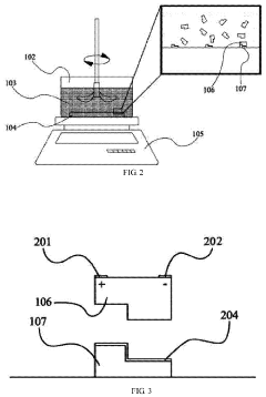
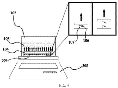
Technical Solution: eLux has developed a proprietary fluidic self-assembly (FSA) approach for microLED mass transfer that leverages surface tension and fluidic forces to achieve high-throughput placement. Their technology, called "Liquid-Pixel," uses a microfluidic delivery system where microLED chips are suspended in a carefully engineered carrier fluid with specific rheological properties[5]. The receptor substrate contains hydrophilic/hydrophobic patterned wells that create localized surface energy differences. When the microLED-containing fluid flows across the substrate, the surface tension forces guide individual chips into their designated receptor sites[6]. eLux has enhanced this basic principle with electrokinetic assistance, where mild electric fields help direct the microLEDs toward their target locations. The company has demonstrated the ability to transfer over 1 million microLEDs per minute using parallel processing across large substrate areas, with their latest generation achieving placement yields above 99% for chips as small as 5μm.
Strengths: Extremely high throughput capability, inherently parallel process that scales efficiently with display size, and minimal mechanical stress on delicate microLED structures. Weaknesses: Requires precise control of fluid properties and flow dynamics, potential for contamination from fluid residues, and challenges with achieving perfect RGB alignment for full-color displays.
BOE Technology Group Co., Ltd.
Technical Solution: BOE has pioneered a hybrid electrostatic-fluidic transfer approach for microLED mass production that combines the advantages of both methodologies. Their system utilizes electrostatically charged microfluidic channels to transport and precisely position microLED chips[2]. The process begins with microLEDs suspended in a specially formulated dielectric fluid with controlled viscosity and dielectric properties. Electrode arrays generate non-uniform electric fields that create dielectrophoretic forces, guiding the microLEDs through microfluidic pathways toward receptor sites[4]. BOE's technology incorporates a multi-stage transfer process with sequential alignment stations that progressively improve placement accuracy. The company has also developed proprietary surface treatments for both microLEDs and substrate materials to optimize adhesion forces during the final placement phase. This approach enables transfer rates of approximately 30 million units per hour with placement accuracy within 2μm.
Strengths: Excellent scalability for different display sizes, reduced mechanical stress on microLED chips compared to pure mechanical methods, and high transfer yield (>99%) across RGB chips. Weaknesses: Complex system integration requiring precise synchronization between fluidic and electrostatic components, and potential for fluid contamination affecting long-term reliability of transferred microLEDs.
Critical Patents in MicroLED Transfer Methods
Micro light-emitting diode mass transfer apparatus and method
PatentActiveUS20210384050A1
Innovation
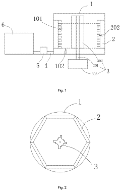
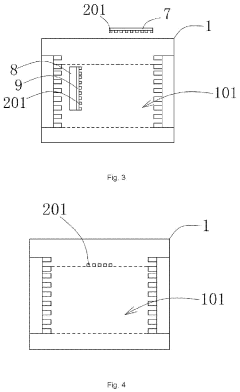
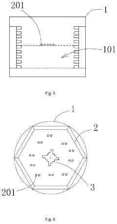
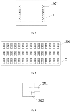
- A micro LED mass transfer apparatus and method using a solution container with a transfer solution, where micro LEDs float and are driven into chip mounting cells on display backplanes by centrifugal force, facilitated by a solution drive assembly and liquid level control, allowing for precise and efficient transfer with simple devices.
Mass transfer method for micro-leds with a temperature-controlled adhesive layer
PatentActiveUS20200203558A1
Innovation
- A mass transfer method utilizing a temperature-controlled adhesive layer on a transfer substrate with self-assembling microstructures that becomes sticky at temperatures above 40°C and loses stickiness below 25°C, allowing for reversible and repeatable attachment and detachment of Micro-LED dies, enabling efficient and precise transfer without electromagnetic interference.
Manufacturing Scalability Assessment
The scalability of manufacturing processes for microLED mass transfer using electrostatic and fluidic approaches represents a critical factor in determining commercial viability. Current manufacturing capabilities demonstrate significant variations in throughput rates, with electrostatic transfer methods achieving transfer rates of approximately 10,000-50,000 units per hour under optimal conditions. Fluidic approaches, while showing promise in laboratory settings, currently operate at lower throughput rates of 5,000-20,000 units per hour but offer advantages in handling smaller microLED sizes.
Equipment scaling considerations reveal that electrostatic transfer systems require substantial capital investment, with typical production-scale equipment costing between $2-5 million per installation. These systems occupy considerable cleanroom space, typically requiring 50-100 square meters per production line. Fluidic systems, though less established at industrial scale, potentially offer more compact footprints at 30-60 square meters but face challenges in process control standardization.
Yield analysis indicates that electrostatic approaches currently achieve 99.5% placement accuracy in controlled environments, with defect rates below 0.5% for LEDs larger than 30μm. However, this performance degrades significantly for sub-10μm devices. Fluidic approaches demonstrate more consistent performance across size ranges but with slightly lower overall yield rates of 98-99% in current implementations.
Cost modeling projections suggest that at volumes exceeding 1 million devices per day, electrostatic approaches offer a cost advantage of approximately $0.05-0.10 per transferred microLED. This advantage diminishes at lower production volumes due to fixed equipment costs. Fluidic approaches show more favorable economics at smaller batch sizes but currently lack the maturity for high-volume production environments.
Integration with existing semiconductor manufacturing infrastructure presents varying challenges. Electrostatic approaches benefit from compatibility with established pick-and-place equipment architectures, allowing for adaptation of existing production lines with moderate modifications. Fluidic approaches require more specialized equipment but potentially offer better integration with wafer-level processing techniques common in semiconductor fabrication.
Future scaling trajectories indicate that electrostatic transfer technologies could reach throughput rates of 100,000+ units per hour within 2-3 years through parallelization and process optimization. Fluidic approaches show potential for exponential improvement, with laboratory demonstrations suggesting possible throughput rates exceeding 200,000 units per hour, though commercial implementation remains several years from realization.
Environmental Impact of Transfer Processes
The environmental impact of microLED mass transfer processes represents a critical consideration as this technology moves toward widespread commercial adoption. Electrostatic and fluidic approaches, while offering promising solutions for efficient mass transfer, introduce specific environmental concerns that warrant careful examination.
Energy consumption constitutes a primary environmental factor in these transfer processes. Electrostatic methods typically require high-voltage power supplies to generate sufficient electric fields for reliable pick-and-place operations. This energy demand, when scaled to industrial production levels, could result in significant carbon footprints unless powered by renewable energy sources. Fluidic approaches may offer comparatively lower direct energy requirements but often necessitate additional processing steps for fluid management and recovery.
Chemical usage presents another environmental challenge. Fluidic transfer methods frequently employ specialized solutions containing surfactants, stabilizers, and other additives that facilitate precise microLED manipulation. The production, use, and disposal of these chemicals require careful management to prevent environmental contamination. Similarly, electrostatic processes often utilize specialized coatings or surface treatments that may contain potentially hazardous materials requiring proper handling protocols.
Waste generation across the microLED transfer lifecycle demands attention. Both approaches produce various waste streams including spent transfer media, contaminated fluids, and discarded substrate materials. The semiconductor industry's historical challenges with waste management highlight the importance of developing circular economy approaches for these new processes. Particularly concerning are nanomaterials and specialized polymers that may resist conventional degradation pathways.
Water consumption represents a significant concern, especially for fluidic approaches. These methods typically require ultra-pure water for solution preparation and post-transfer cleaning processes. In regions facing water scarcity, this intensive water usage could exacerbate existing resource pressures. Electrostatic methods generally demand less direct water consumption but may still require wet processing steps for preparation and cleaning.
Comparative lifecycle assessments between these transfer technologies remain limited, creating a knowledge gap regarding their comprehensive environmental impacts. Preliminary studies suggest that while electrostatic approaches may offer advantages in energy efficiency and reduced chemical usage, fluidic methods might provide benefits in terms of transfer yield and reduced material waste. The environmental calculus ultimately depends on specific implementation details and production scales.
Emerging regulatory frameworks worldwide increasingly emphasize environmental considerations in manufacturing processes. Companies developing microLED transfer technologies must anticipate stricter environmental standards and design processes accordingly. This proactive approach not only ensures regulatory compliance but potentially creates competitive advantages through sustainable manufacturing practices.
Unlock deeper insights with Patsnap Eureka Quick Research — get a full tech report to explore trends and direct your research. Try now!
Generate Your Research Report Instantly with AI Agent
Supercharge your innovation with Patsnap Eureka AI Agent Platform!