Electronic Transport In Electride Thin Films Measurement Protocols
AUG 28, 20259 MIN READ
Generate Your Research Report Instantly with AI Agent
Patsnap Eureka helps you evaluate technical feasibility & market potential.
Electride Thin Films Background and Research Objectives
Electride materials represent a unique class of compounds where electrons serve as anions, occupying specific positions in the crystal lattice. The concept of electrides was first theorized in the 1960s, but significant experimental progress only emerged in the late 1980s with the synthesis of organic electrides. The field experienced a revolutionary advancement in 2013 with the discovery of stable inorganic electrides, particularly mayenite-based C12A7:e- (12CaO·7Al2O3:e-), which demonstrated stability in ambient conditions.
The evolution of electride research has progressed from bulk materials to thin films, driven by the potential for integration into electronic devices and catalytic applications. Thin film electrides offer advantages in terms of scalability, integration capability, and tunability of electronic properties through thickness control and substrate engineering. This transition represents a critical step toward practical applications of these materials in next-generation electronics and energy technologies.
Current research objectives in electride thin films focus on several key areas. First, developing reliable and reproducible synthesis methods for high-quality electride thin films with controlled thickness and composition. Common approaches include pulsed laser deposition (PLD), molecular beam epitaxy (MBE), and magnetron sputtering, each presenting unique challenges in maintaining the electride state during deposition.
Second, establishing standardized protocols for measuring electronic transport properties in these films represents a critical research goal. The unusual electronic structure of electrides, with their localized anionic electrons, creates unique challenges for conventional measurement techniques. Understanding how to accurately characterize parameters such as carrier concentration, mobility, and conductivity mechanisms is essential for advancing the field.
Third, researchers aim to elucidate the fundamental relationship between structural characteristics and electronic properties in electride thin films. This includes investigating the effects of film thickness, crystallinity, defect concentration, and interfacial phenomena on electronic transport behavior.
Finally, there is significant interest in exploring novel electride compositions and heterostructures to expand the range of accessible properties and functionalities. This includes developing new synthesis routes for previously theoretical electride compounds and creating multilayer structures that combine electrides with other functional materials to achieve enhanced or entirely new properties.
The ultimate goal of this research direction is to establish electride thin films as a viable platform for next-generation electronic devices, catalysts, and energy conversion systems, leveraging their unique electronic structure and properties.
Market Applications and Demand Analysis for Electride Materials
The electride materials market is experiencing significant growth driven by their unique electronic properties, particularly their ability to emit electrons with minimal energy input. The global market for advanced electronic materials, including electrides, is projected to reach $12.7 billion by 2025, with a compound annual growth rate of 8.3% from 2020. This growth is primarily fueled by increasing demand for energy-efficient electronic components and catalysts across multiple industries.
In the semiconductor industry, electride thin films show promising applications in next-generation electronic devices. Their exceptional electron mobility characteristics make them potential candidates for high-speed transistors and memory devices. Major semiconductor manufacturers are exploring electride integration into their technology roadmaps, particularly for applications requiring low power consumption and high performance.
The energy sector represents another significant market for electride materials. Their catalytic properties make them valuable for ammonia synthesis and hydrogen production applications, potentially reducing energy requirements by up to 40% compared to conventional catalysts. This efficiency improvement translates to substantial cost savings and environmental benefits in industrial processes.
Display technology manufacturers have shown increasing interest in electride thin films for advanced display applications. The unique electron emission properties of electrides make them suitable for field emission displays and other electron emission-based technologies. Market research indicates that the advanced display materials segment is growing at 9.7% annually, with electrides positioned to capture a portion of this expanding market.
Aerospace and defense industries are exploring electride applications in specialized electronic components that must operate in extreme environments. The stability and performance characteristics of certain electride compositions under challenging conditions make them valuable for mission-critical applications where conventional materials fail.
Research institutions and material science companies are the primary consumers of electride materials currently, with demand focused on measurement protocols and characterization techniques. This research-driven demand is expected to transition to commercial applications within 3-5 years as manufacturing processes mature and costs decrease.
Geographical analysis shows that Asia-Pacific, particularly Japan, China, and South Korea, leads in electride research and potential commercial applications, followed by North America and Europe. This regional distribution aligns with centers of electronics manufacturing and advanced materials research.
Market barriers include high production costs, scalability challenges, and limited standardization of measurement protocols. As these barriers are addressed through ongoing research efforts like those focused on electronic transport measurement standardization, market penetration is expected to accelerate significantly.
Current Challenges in Electronic Transport Measurement
Despite significant advancements in electride thin film fabrication, electronic transport measurements in these materials face substantial technical challenges. The unique electron configuration of electrides, where electrons serve as anions without being bound to specific atomic nuclei, creates measurement complexities not encountered in conventional materials. Current measurement protocols struggle with the extreme sensitivity of electride surfaces to environmental conditions, particularly oxygen and moisture exposure, which can rapidly degrade their electronic properties and compromise measurement accuracy.
Sample preparation represents a critical bottleneck in the measurement process. The ultra-high vacuum conditions required for maintaining electride stability during measurements necessitate specialized equipment that is not widely available. Additionally, the interface between measurement probes and electride surfaces introduces contact resistance issues that can dominate and obscure the intrinsic electronic transport properties researchers aim to measure.
Temperature-dependent measurements present another significant challenge. Many electrides exhibit dramatic changes in their electronic structure across different temperature ranges, requiring measurement systems capable of maintaining stable conditions from cryogenic temperatures to several hundred degrees Celsius while simultaneously performing precise electrical measurements. The thermal expansion mismatch between electride films and measurement apparatus can induce mechanical stress, potentially altering the material's electronic properties during measurement.
The thickness-dependent properties of electride thin films further complicate measurement protocols. As film thickness approaches the nanometer scale, quantum confinement effects become pronounced, necessitating measurement techniques that can distinguish between bulk and surface transport mechanisms. Current methodologies often lack the spatial resolution to effectively separate these contributions.
Reproducibility remains a persistent issue in the field. The extreme sensitivity of electrides to preparation conditions means that seemingly identical samples can exhibit substantially different transport properties. This variability makes it difficult to establish standardized measurement protocols and complicates the comparison of results between different research groups.
Advanced characterization techniques such as Hall effect measurements and magnetoresistance studies face implementation challenges in electride systems due to their unusual carrier dynamics. The conventional models used to interpret these measurements may not accurately capture the behavior of anionic electrons in electrides, leading to potential misinterpretation of experimental data.
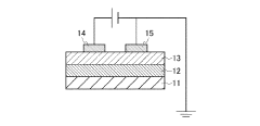
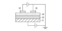
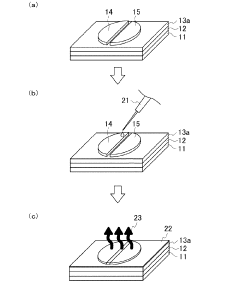
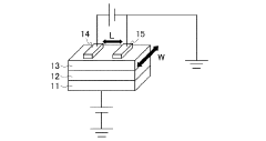
Established Protocols for Electronic Transport Measurements
01 Fabrication methods for electride thin films
Various techniques are employed to fabricate electride thin films with controlled electronic transport properties. These methods include vapor deposition, sputtering, and epitaxial growth processes that enable precise control over film thickness, composition, and crystallinity. The fabrication processes often involve specific temperature and pressure conditions to achieve the desired electride structure where electrons serve as anions. These techniques are crucial for developing electride films with optimal electronic transport characteristics for various applications.- Electride thin film fabrication methods: Various methods for fabricating electride thin films have been developed to achieve specific electronic transport properties. These methods include vapor deposition techniques, sputtering, and epitaxial growth processes that allow precise control over film thickness and composition. The fabrication techniques focus on creating stable electride structures where electrons serve as anions, resulting in unique electronic transport characteristics essential for advanced electronic applications.
- Electronic transport mechanisms in electride materials: Electride thin films exhibit distinctive electronic transport mechanisms characterized by electrons localized in structural cavities rather than bound to atoms. These materials demonstrate high electron mobility, low work function, and unique conductivity properties that differ significantly from conventional conductors and semiconductors. The transport properties can be tuned by controlling the structural parameters and composition of the electride films, enabling customization for specific electronic applications.
- Composition and structure optimization for enhanced conductivity: The electronic transport properties of electride thin films can be significantly enhanced through optimization of their composition and crystal structure. Incorporating specific elements or compounds, controlling defect concentrations, and engineering the crystal lattice can lead to improved conductivity and carrier mobility. Research has focused on developing electride materials with optimal electron concentration in interstitial spaces to maximize electronic transport efficiency while maintaining structural stability.
- Temperature and environmental effects on electride performance: The electronic transport properties of electride thin films are significantly influenced by temperature variations and environmental conditions. Studies have investigated how thermal fluctuations affect electron mobility and conductivity in these materials. Additionally, research has examined the stability of electride films under various atmospheric conditions, as exposure to oxygen, moisture, or other reactive species can alter their electronic properties. Understanding these effects is crucial for developing electride-based devices that can operate reliably under real-world conditions.
- Applications of electride thin films in electronic devices: Electride thin films with their unique electronic transport properties have found applications in various electronic and optoelectronic devices. These materials are being utilized in field emission displays, electron emitters, transparent conductors, and catalytic applications. The low work function and high electron mobility of electride films make them particularly suitable for electron injection layers in devices. Recent research has focused on integrating these materials into next-generation electronic components to take advantage of their distinctive electronic transport characteristics.
02 Electronic transport mechanisms in electride materials
Electride thin films exhibit unique electronic transport mechanisms due to their structure where electrons act as anions. These materials demonstrate distinctive conductivity behaviors, including temperature-dependent transport properties and quantum confinement effects in thin film geometries. The transport mechanisms are characterized by high electron mobility, low work function, and unusual carrier concentration behaviors. Understanding these mechanisms is essential for developing electride-based electronic devices with enhanced performance characteristics.Expand Specific Solutions03 Composition and structure engineering for enhanced properties
The electronic transport properties of electride thin films can be significantly enhanced through composition and structure engineering. By incorporating specific dopants, creating layered structures, or controlling defect concentrations, researchers can tune the electronic band structure and carrier concentration. Optimization of the crystal structure and interfaces between layers plays a crucial role in determining the overall electronic transport behavior. These engineering approaches enable the development of electride films with tailored properties for specific applications.Expand Specific Solutions04 Characterization techniques for electride thin films
Advanced characterization techniques are essential for analyzing the electronic transport properties of electride thin films. These include Hall effect measurements, scanning tunneling microscopy, angle-resolved photoemission spectroscopy, and various electrical conductivity testing methods. Temperature-dependent measurements provide insights into transport mechanisms, while spectroscopic techniques reveal electronic structure details. These characterization approaches are crucial for understanding structure-property relationships in electride materials and optimizing their performance for electronic applications.Expand Specific Solutions05 Applications of electride thin films in electronic devices
Electride thin films with their unique electronic transport properties find applications in various electronic devices. These include field-effect transistors, electron emitters, transparent conductive electrodes, and sensors. The low work function and high electron mobility of electride films make them particularly suitable for electron emission applications and energy conversion devices. Their stability under various operating conditions and compatibility with existing semiconductor processing techniques further enhance their potential for next-generation electronic technologies.Expand Specific Solutions
Leading Research Groups and Industrial Players in Electride Technology
The electronic transport measurement in electride thin films represents an emerging field at the intersection of materials science and electronics. Currently in its early development stage, this technology is characterized by a growing but still limited market size, with significant research activity but limited commercial applications. The technical maturity varies across key players, with research institutions like Tsinghua University and Max Planck Society leading fundamental research, while companies such as Samsung Electronics, Applied Materials, and Lam Research are developing practical applications and measurement protocols. Hitachi and Sumitomo Chemical are advancing materials characterization techniques, while Nova Ltd. and Excelitas focus on specialized measurement instrumentation. The field is transitioning from academic research to industrial implementation, with semiconductor and electronics manufacturers increasingly investing in electride technology for next-generation electronic devices.
Hitachi Ltd.
Technical Solution: Hitachi has developed advanced measurement protocols for electronic transport in electride thin films using their proprietary scanning probe microscopy (SPM) technologies. Their approach combines atomic force microscopy (AFM) with specialized conductive probes to measure local electronic properties at nanoscale resolution. Hitachi's system incorporates temperature-controlled sample stages (4K to 800K) allowing for temperature-dependent transport measurements critical for understanding electride behavior. Their protocol includes multi-point probe configurations that enable simultaneous measurement of Hall effect, magnetoresistance, and thermoelectric properties in ultra-thin electride films. Hitachi has also developed specialized sample preparation techniques to maintain the air-sensitive nature of many electride materials, using controlled atmosphere transfer systems between deposition chambers and measurement apparatus. Their data acquisition system incorporates real-time filtering algorithms to improve signal-to-noise ratios for the often weak electronic signals from atomically thin electride layers.
Strengths: Superior nanoscale spatial resolution allowing for mapping of electronic transport variations across thin films. Comprehensive temperature-dependent measurement capabilities provide insights into transport mechanisms. Weaknesses: Equipment complexity requires significant expertise to operate effectively. High cost of implementation limits accessibility to specialized research facilities.
Tsinghua University
Technical Solution: Tsinghua University has developed innovative measurement protocols for electronic transport in electride thin films with a focus on operando characterization under various environmental conditions. Their approach combines traditional transport measurements with in-situ X-ray photoelectron spectroscopy (XPS) to correlate electronic properties with surface chemical states during exposure to controlled atmospheres. Tsinghua's protocol incorporates custom-designed microfluidic cells that enable electronic transport measurements while exposing electride films to various gases or liquids, critical for understanding environmental stability and sensing applications. They've pioneered the use of scanning electrochemical microscopy specifically adapted for electride materials, allowing simultaneous mapping of electronic and electrochemical properties with micron resolution. Their measurement system includes capabilities for pressure-dependent transport studies (vacuum to 100 atm), revealing how mechanical stress affects the unique electron confinement in electride structures. Tsinghua researchers have also developed specialized impedance spectroscopy protocols that can separate bulk, grain boundary, and interface contributions to electronic transport in polycrystalline electride films.
Strengths: Excellent capabilities for studying environmental interactions and stability of electride films. Comprehensive correlation between electronic properties and chemical states. Weaknesses: Complex multi-modal measurements require significant expertise to interpret correctly. Some specialized setups have limited throughput for routine measurements.
Critical Analysis of Advanced Measurement Methodologies
Thin film, method for manufacturing thin film, and product comprising thin film
PatentInactiveJP2020063177A
Innovation
- A thin film comprising metal atoms or ions and a π-electron conjugated substance, where the metal atoms or ions are dispersed on the surface of the π-electron conjugated substance, is produced by a method involving a complex-containing droplet dropping step and a ligand removal step.
Compressed fluid formulation containing electron transporting material
PatentInactiveUS20040108510A1
Innovation
- A compressed fluid formulation containing an electron transporting material, such as Alq3, is used, where the material is dissolved, dispersed, or solubilized in a compressed fluid, allowing for solvent-free deposition and forming a solid film, enabling precise and high-speed patterning without the need for prepatterned substrates or evaporation steps.
Standardization Efforts in Electride Measurement Protocols
The standardization of measurement protocols for electride thin films represents a critical frontier in advancing the field of electronic transport studies. Currently, the research community faces significant challenges due to the lack of universally accepted methodologies, which has led to inconsistencies in reported data and difficulties in cross-laboratory validation of results.
Several international organizations have begun coordinating efforts to establish standardized measurement protocols specifically for electride materials. The International Union of Pure and Applied Chemistry (IUPAC) has formed a dedicated working group focused on developing guidelines for the characterization of electron-localized materials, with electrides being a primary focus. This initiative aims to create a comprehensive framework that addresses the unique challenges posed by these materials.
The IEEE Standards Association has also launched a project to standardize electronic transport measurements in novel materials, with a dedicated subsection on electride thin films. Their approach emphasizes reproducibility and reliability, particularly addressing the sensitivity of electrides to environmental conditions such as oxygen exposure and humidity.
A notable advancement in standardization has been the recent publication of the "Electride Characterization Protocol" (ECP) by a consortium of leading research institutions. The ECP outlines specific procedures for sample preparation, handling, and measurement techniques tailored to the unique properties of electrides. This protocol recommends controlled environment chambers with precise oxygen and moisture monitoring for all measurements, standardized electrode configurations, and specific temperature ramping rates to ensure consistent results.
Industry participation has been crucial in these standardization efforts. Companies developing electride-based technologies have contributed proprietary data to help establish baseline performance metrics and acceptable variation ranges. This collaboration between academia and industry has accelerated the development of practical standards that balance scientific rigor with industrial applicability.
Regional differences in standardization approaches present an ongoing challenge. Asian research institutions, particularly in Japan and China where significant electride research is conducted, have developed protocols that sometimes differ from those proposed by European and North American entities. Efforts to harmonize these regional standards are underway through international conferences and collaborative research initiatives.
The timeline for full implementation of standardized protocols remains uncertain, with most experts projecting a 3-5 year horizon before comprehensive standards are widely adopted. In the interim, many research publications have begun including detailed methodological appendices that specify exact measurement conditions, representing an important step toward greater reproducibility in the field.
Environmental Stability and Scalability Considerations
Electride thin films present unique challenges regarding environmental stability and scalable production that must be addressed for practical applications. These materials, characterized by their anionic electrons occupying interstitial sites, typically demonstrate high reactivity with atmospheric components, particularly oxygen and water vapor. Exposure to ambient conditions often leads to rapid degradation of their electronic properties, with some electrides showing complete loss of functionality within minutes of air exposure. This instability necessitates specialized handling protocols, including inert atmosphere processing and encapsulation techniques.
Current stability enhancement strategies include protective capping layers using materials such as Al2O3, HfO2, or h-BN that provide effective oxygen and moisture barriers while maintaining electrical contact with the electride layer. Recent advancements have demonstrated extended stability periods of up to several weeks for properly encapsulated Ca2N and Y-doped BaO thin films, representing significant progress from earlier generations that degraded within hours.
The scalability of electride thin film production presents another critical consideration. Laboratory-scale synthesis methods such as molecular beam epitaxy (MBE) and pulsed laser deposition (PLD) produce high-quality films but face significant challenges in scaling to industrial dimensions. These challenges include maintaining stoichiometric precision, structural uniformity, and crystalline quality across larger substrates. Alternative approaches using modified sputtering techniques have shown promise for larger-area deposition but typically result in films with reduced carrier mobility.
Temperature sensitivity during processing represents another scalability hurdle, as many electride materials require precise thermal conditions to form their characteristic electron-localized structures. Deviations of even 10-15°C can significantly alter electronic transport properties, necessitating advanced temperature control systems for industrial-scale production.
Standardized measurement protocols must account for these stability and scalability factors. This includes establishing baseline degradation rates under controlled exposure conditions, quantifying the effectiveness of various encapsulation methods, and developing accelerated aging tests that can predict long-term stability. For scalability assessment, measurement protocols should incorporate uniformity mapping across larger substrates and statistical process control metrics to ensure consistency in electronic transport properties.
Recent collaborative efforts between research institutions and semiconductor manufacturers have begun establishing industry standards for electride thin film characterization that specifically address these environmental stability and scalability considerations, potentially accelerating their integration into practical electronic devices.
Unlock deeper insights with Patsnap Eureka Quick Research — get a full tech report to explore trends and direct your research. Try now!
Generate Your Research Report Instantly with AI Agent
Supercharge your innovation with Patsnap Eureka AI Agent Platform!