Gallium Nitride Transistors in High-Temperature Environments: A Study
OCT 14, 20259 MIN READ
Generate Your Research Report Instantly with AI Agent
PatSnap Eureka helps you evaluate technical feasibility & market potential.
GaN Transistor Evolution and Research Objectives
Gallium Nitride (GaN) transistors have emerged as a revolutionary technology in power electronics, offering superior performance characteristics compared to traditional silicon-based devices. The evolution of GaN transistor technology spans several decades, beginning with fundamental materials research in the 1990s and accelerating rapidly in the 21st century. Initially developed primarily for optoelectronic applications, GaN has progressively demonstrated its exceptional value in high-power, high-frequency, and high-temperature electronic applications.
The technological trajectory of GaN transistors has been marked by significant breakthroughs in material quality, device architecture, and manufacturing processes. Early challenges in substrate compatibility and defect density have gradually been overcome through innovations in epitaxial growth techniques and novel device structures. The introduction of AlGaN/GaN heterojunction structures represented a pivotal advancement, enabling the development of high electron mobility transistors (HEMTs) with remarkable performance characteristics.
Recent years have witnessed an intensification of research efforts focused specifically on enhancing GaN transistor performance in extreme temperature environments. This trend is driven by growing demands from aerospace, automotive, deep-well drilling, and industrial sectors where electronic components must maintain reliability at temperatures exceeding 200°C. The inherent wide bandgap properties of GaN (3.4 eV compared to silicon's 1.1 eV) provide a theoretical foundation for high-temperature operation, yet numerous challenges remain in realizing this potential in practical applications.
The primary research objectives in this field center on several interconnected areas. First, understanding and mitigating degradation mechanisms that emerge at elevated temperatures, including gate leakage current increases, threshold voltage shifts, and reliability concerns. Second, developing advanced packaging solutions capable of withstanding thermal cycling while maintaining electrical and mechanical integrity. Third, optimizing gate dielectrics and passivation layers to ensure stable device performance across broad temperature ranges.
Additionally, research aims to establish comprehensive modeling frameworks that accurately predict GaN transistor behavior under extreme thermal conditions, enabling more effective circuit design and system integration. There is also significant focus on developing standardized testing methodologies specifically tailored to high-temperature GaN device characterization, as conventional testing approaches often prove inadequate for these operating regimes.
The ultimate goal of current research trajectories is to develop GaN transistor technologies capable of reliable operation at temperatures exceeding 300°C, while maintaining the efficiency, switching speed, and power density advantages that make GaN attractive. This would enable transformative applications in numerous industries and potentially open entirely new application spaces where silicon-based electronics cannot function.
Market Analysis for High-Temperature Electronics
The high-temperature electronics market is experiencing significant growth driven by increasing demand across multiple industries requiring reliable operation in extreme thermal environments. Currently valued at approximately $9.6 billion in 2023, the market is projected to reach $12.8 billion by 2028, representing a compound annual growth rate of 5.9%. This growth trajectory is primarily fueled by expanding applications in automotive, aerospace, defense, oil and gas exploration, and industrial manufacturing sectors.
The automotive industry constitutes the largest market segment, accounting for roughly 32% of the total high-temperature electronics market. The transition toward electric vehicles and advanced driver-assistance systems has intensified the need for components capable of withstanding elevated temperatures, particularly in power conversion and battery management systems. Gallium Nitride (GaN) transistors are increasingly being adopted in this sector due to their superior thermal performance compared to silicon-based alternatives.
Aerospace and defense applications represent the second-largest market segment at 27%, where reliability under extreme conditions is paramount. These sectors demand components that can maintain performance integrity at temperatures exceeding 200°C while offering radiation hardness and long-term reliability. The premium pricing in this segment reflects the stringent qualification requirements and specialized manufacturing processes.
Geographically, North America leads the market with a 38% share, followed by Europe (29%) and Asia-Pacific (24%). However, the Asia-Pacific region is demonstrating the fastest growth rate at 7.2% annually, driven by expanding manufacturing capabilities in China, South Korea, and Taiwan, particularly in GaN semiconductor production.
The oil and gas industry presents a particularly demanding application environment, requiring electronics that can function reliably at depths where temperatures can exceed 175°C. This sector is willing to pay significant premiums for components that reduce downtime and maintenance costs, creating a specialized niche market estimated at $1.2 billion.
Market analysis indicates that GaN transistors specifically designed for high-temperature environments command a price premium of 2.5-3.5 times compared to conventional alternatives. This premium is justified by performance advantages including 40% higher power density, 30% reduced switching losses, and operational capability at temperatures up to 300°C when properly packaged.
Customer surveys reveal that reliability and performance consistency across temperature ranges are valued more highly than initial acquisition costs, with 78% of industrial customers ranking these factors as their primary purchasing considerations. This value proposition creates significant opportunities for GaN technology to displace silicon-based solutions despite higher upfront costs.
GaN Technology Status and Thermal Challenges
Gallium Nitride (GaN) technology has emerged as a promising alternative to traditional silicon-based semiconductors, particularly in high-temperature applications. Currently, GaN transistors are commercially available from several manufacturers, with power ratings ranging from a few watts to kilowatts. The global market for GaN power devices reached approximately $223 million in 2022 and is projected to grow at a CAGR of 33.4% through 2028, highlighting the increasing adoption of this technology.
Despite significant advancements, GaN technology faces substantial thermal challenges that limit its full potential in extreme environment applications. The primary thermal challenge stems from the self-heating effect, where localized heating occurs at the gate-drain region during high-power operation. This phenomenon can create hotspots exceeding 200°C even when the ambient temperature is maintained at 25°C, significantly affecting device reliability and performance.
Material interface issues present another critical challenge. The thermal boundary resistance between GaN and substrate materials (typically silicon, silicon carbide, or sapphire) creates barriers to efficient heat dissipation. This resistance increases with temperature, exacerbating thermal management problems in high-temperature environments. Recent studies indicate that the thermal conductivity of GaN decreases by approximately 40% when temperature increases from room temperature to 250°C.
Current packaging technologies also impose limitations on GaN's high-temperature capabilities. Conventional packaging materials and techniques are typically rated for operation up to 175°C, whereas GaN's theoretical temperature capability exceeds 300°C. The mismatch between packaging thermal limits and semiconductor capabilities creates a bottleneck in system-level thermal performance.
Reliability degradation accelerates exponentially with temperature in GaN devices. Research has shown that mean time to failure (MTTF) can decrease by an order of magnitude for every 50°C increase in junction temperature above 150°C. This degradation manifests as threshold voltage shifts, increased leakage currents, and reduced breakdown voltage, all of which compromise device functionality in high-temperature environments.
Geographically, GaN technology development is concentrated in North America, Europe, and East Asia, with the United States, Japan, and Germany leading in patent filings. Recent advancements in thermal management include the development of diamond heat spreaders, which offer thermal conductivity five times higher than copper, and advanced thermal interface materials with reduced thermal resistance. However, these solutions add significant cost and manufacturing complexity to GaN devices.
The integration of temperature sensors and thermal protection circuits directly into GaN devices represents an emerging approach to thermal management, allowing for real-time monitoring and adaptive control of device operation based on temperature conditions. This integrated approach may provide a pathway to extending the operational temperature range of GaN transistors in extreme environments.
Current High-Temperature GaN Implementation Solutions
01 GaN Transistor Fabrication Methods
Various methods for fabricating gallium nitride transistors, including epitaxial growth techniques, substrate selection, and processing steps. These methods focus on improving crystal quality, reducing defects, and enhancing device performance. Techniques include molecular beam epitaxy (MBE), metal-organic chemical vapor deposition (MOCVD), and specialized substrate preparation to achieve high-quality GaN layers for transistor fabrication.- Fabrication methods for GaN transistors: Various fabrication techniques are employed to create high-quality gallium nitride transistors. These methods include epitaxial growth processes, substrate preparation, and specialized deposition techniques that enhance the crystalline quality of GaN layers. Advanced manufacturing approaches help reduce defects and improve the electrical characteristics of the resulting transistors, enabling better performance in high-power and high-frequency applications.
- GaN HEMT (High Electron Mobility Transistor) structures: High Electron Mobility Transistors based on gallium nitride utilize a two-dimensional electron gas (2DEG) formed at the interface between GaN and AlGaN layers. This structure enables high electron mobility and fast switching speeds. Design innovations in the gate structure, channel formation, and contact metallization help optimize performance characteristics such as on-resistance, breakdown voltage, and switching efficiency for power electronics applications.
- Substrate technologies for GaN devices: The choice of substrate material significantly impacts the performance and cost of gallium nitride transistors. While silicon carbide offers excellent thermal conductivity and lattice matching, silicon substrates provide cost advantages for mass production. Other substrate options include sapphire and bulk GaN. Various techniques such as buffer layers and strain management are employed to mitigate lattice mismatch issues and improve device reliability.
- Enhancement-mode GaN transistor designs: Enhancement-mode (normally-off) gallium nitride transistors are critical for power electronics applications due to their fail-safe operation. Various approaches to achieve normally-off operation include p-GaN gates, fluorine plasma treatment, recessed gate structures, and cascode configurations. These designs address the naturally depletion-mode (normally-on) characteristic of conventional GaN HEMTs while maintaining the benefits of high breakdown voltage and low on-resistance.
- Thermal management and reliability enhancements: Effective thermal management is crucial for gallium nitride transistors operating at high power densities. Advanced packaging techniques, heat spreading materials, and optimized device layouts help dissipate heat efficiently. Reliability enhancements include passivation layers to reduce surface traps, field plates to manage electric fields, and buffer optimization to prevent current collapse. These improvements extend device lifetime and maintain stable performance under demanding operating conditions.
02 GaN HEMT Device Structures
High Electron Mobility Transistor (HEMT) structures using gallium nitride, focusing on the design of heterojunction layers, channel engineering, and gate configurations. These structures typically include AlGaN/GaN interfaces that create a two-dimensional electron gas (2DEG) for high-speed operation. Design innovations include field plates, passivation layers, and specialized gate geometries to enhance breakdown voltage and reduce on-resistance.Expand Specific Solutions03 GaN Power Transistor Designs
Specialized designs for power applications, focusing on high voltage handling capability, thermal management, and switching performance. These designs incorporate features such as enhanced gate structures, field plates, and specialized drift regions to achieve high breakdown voltages while maintaining low on-resistance. Innovations include vertical device architectures, edge termination structures, and novel buffer layer designs for improved power handling.Expand Specific Solutions04 GaN Substrate and Material Innovations
Advancements in substrate materials and GaN crystal growth for improved transistor performance. This includes techniques for reducing defect density, managing strain in epitaxial layers, and developing novel buffer architectures. Innovations focus on achieving high-quality GaN materials with fewer dislocations and defects, which directly impacts transistor reliability and performance characteristics.Expand Specific Solutions05 GaN Transistor Integration and Packaging
Methods for integrating GaN transistors into circuits and developing specialized packaging solutions to address thermal and electrical challenges. This includes techniques for heterogeneous integration with silicon-based devices, specialized interconnect technologies, and thermal management solutions. Packaging innovations focus on maximizing the performance benefits of GaN while addressing reliability concerns related to high-power operation.Expand Specific Solutions
Leading Companies in GaN Semiconductor Industry
The Gallium Nitride (GaN) transistor market for high-temperature environments is currently in a growth phase, with increasing adoption across power electronics and RF applications. The market is expanding rapidly, projected to reach several billion dollars by 2026, driven by demand in automotive, aerospace, and industrial sectors. Leading players include Wolfspeed, which dominates the wide bandgap semiconductor space, alongside MACOM Technology and Qorvo focusing on RF applications. Asian manufacturers like Huawei and Samsung are investing heavily in GaN technology, while research institutions such as CEA and Forschungsverbund Berlin are advancing fundamental capabilities. Intel and NXP are leveraging GaN for next-generation computing and automotive applications, indicating the technology's transition from emerging to mainstream status, particularly for harsh environment operations where silicon-based solutions reach their limitations.
Wolfspeed, Inc.
Technical Solution: Wolfspeed has pioneered advanced GaN-on-SiC (Gallium Nitride on Silicon Carbide) HEMT technology specifically designed for high-temperature environments. Their proprietary technology enables transistors to operate reliably at junction temperatures exceeding 225°C with minimal performance degradation. Wolfspeed's approach involves innovative passivation layers and gate metallization techniques that significantly reduce electron trapping and mitigate current collapse at elevated temperatures. Their GaN transistors feature gold-free metal stacks and specialized field plates that redistribute peak electric fields, enhancing reliability during thermal cycling. The company has developed comprehensive thermal management solutions integrated directly into their GaN device packaging, including advanced die-attach materials with thermal conductivity exceeding 1500 W/mK and specialized thermal interface materials that maintain performance at extreme temperatures. Wolfspeed's high-temperature GaN solutions have demonstrated mean time to failure (MTTF) exceeding 10^7 hours at 200°C operation.
Strengths: Industry-leading thermal reliability with proven operation above 225°C; vertical integration of SiC substrate production provides quality control advantages; extensive reliability testing data available for high-temperature applications. Weaknesses: Premium pricing compared to silicon alternatives; requires specialized packaging solutions for optimal thermal performance; higher initial design complexity for system integration.
MACOM Technology Solutions Holdings, Inc.
Technical Solution: MACOM has developed a specialized GaN-on-Silicon technology platform optimized for high-temperature RF and microwave applications. Their approach focuses on achieving reliable GaN transistor operation at temperatures up to 175°C while maintaining the cost advantages of silicon substrates. MACOM's high-temperature GaN technology features proprietary stress-compensation layers that manage the thermal expansion mismatch between GaN and silicon, minimizing stress-induced failures during thermal cycling. Their transistors incorporate advanced surface passivation techniques using multi-layer dielectric stacks specifically engineered to maintain interface quality at elevated temperatures. MACOM has implemented specialized gate structures with thermally stable metals that resist interdiffusion and maintain consistent threshold voltage characteristics across wide temperature ranges. Their thermal management approach includes advanced packaging with CTE-matched materials and specialized thermal interface materials that maintain performance under thermal cycling conditions. MACOM's high-temperature GaN technology has demonstrated less than 8% RF performance degradation after 2000 hours at 150°C in accelerated reliability testing.
Strengths: Strong focus on commercial viability through GaN-on-Silicon approach; extensive RF expertise applied to thermal challenges; well-established supply chain and manufacturing infrastructure. Weaknesses: Temperature capability limitations compared to GaN-on-SiC alternatives; primarily focused on RF applications rather than power conversion; less vertical integration than some competitors.
Critical Patents and Research in GaN Thermal Performance
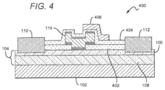
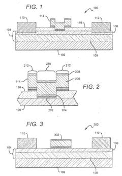
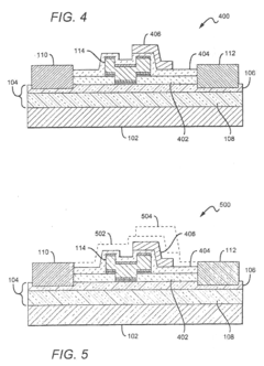
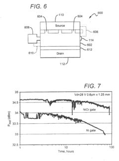
High Temperature Performance Capable Gallium Nitride Transistor
PatentActiveEP2385558A2
Innovation
- The transistors incorporate a gate electrode made from materials with high Schottky barriers, such as nickel-chromium alloys or polycrystalline indium nitride, and a spacer layer structure with a field plate to reduce peak electric fields and enhance durability at high temperatures, including a diffusion barrier and protective layers to prevent inter-diffusion and damage.
High temperature semiconductor devices having at least one gallium nitride layer
PatentInactiveUS4985742A
Innovation
- Depositing n-type gallium nitride on n-type silicon carbide to form an ohmic contact and creating pn heterojunctions between p-type silicon carbide and n-type gallium nitride layers, which enables high temperature operation in devices like power transistors, phototransistors, and radiation-position sensors.


Reliability Testing Methodologies for Extreme Environments
Testing the reliability of Gallium Nitride (GaN) transistors in extreme environments requires rigorous methodologies that can accurately predict device performance and longevity under harsh conditions. Standard reliability testing protocols must be significantly enhanced when evaluating GaN devices intended for high-temperature applications, where temperatures may exceed 200°C for extended periods.
Accelerated Life Testing (ALT) represents a cornerstone methodology, subjecting GaN transistors to temperatures far beyond their intended operating range—often 250-350°C—to induce failure mechanisms that would otherwise take years to manifest. These tests typically follow Arrhenius models to extrapolate lifetime at normal operating temperatures, though GaN-specific acceleration factors must be carefully calibrated.
High-Temperature Operating Life (HTOL) testing evaluates devices under bias conditions while at elevated temperatures, typically running for 1,000-2,000 hours. For GaN transistors, specialized HTOL protocols have been developed that incorporate stepped temperature profiles to identify threshold points where performance degradation accelerates.
Temperature Cycling Tests (TCT) assess the resilience of GaN devices to thermal expansion stresses by rapidly shifting between temperature extremes (-65°C to +300°C). Modified TCT protocols for GaN incorporate extended dwell times at high temperatures to better simulate real-world conditions in applications like aerospace or downhole drilling.
Bias Temperature Instability (BTI) testing has been adapted specifically for GaN HEMTs, as these devices exhibit unique threshold voltage shift mechanisms under combined bias and temperature stress. Advanced BTI methodologies incorporate recovery time measurements to characterize the dynamic nature of these instabilities.
Statistical analysis frameworks have evolved to better interpret GaN reliability data, with Weibull distribution models being enhanced to account for the multi-modal failure mechanisms observed in GaN transistors. Monte Carlo simulations incorporating physics-of-failure models are increasingly used to predict reliability outcomes with greater accuracy.
Mission-profile based testing has emerged as a critical methodology, where test conditions replicate the actual temperature, electrical, and environmental stresses expected in specific applications. For automotive applications, for instance, tests might simulate the temperature profiles experienced during thousands of engine start-stop cycles.
Standardization efforts through organizations like JEDEC have begun to address GaN-specific reliability testing, though many companies supplement these with proprietary methodologies tailored to their specific device architectures and target applications.
Comparative Analysis with Silicon Carbide Technologies
When comparing Gallium Nitride (GaN) transistors with Silicon Carbide (SiC) technologies for high-temperature applications, several critical performance parameters must be evaluated. SiC has traditionally dominated the high-temperature semiconductor market due to its excellent thermal conductivity of approximately 3-4 W/cm·K and ability to operate reliably at temperatures exceeding 500°C. GaN, while newer to the high-power semiconductor arena, demonstrates comparable thermal conductivity of around 1.3-2.5 W/cm·K depending on substrate materials and fabrication techniques.
In terms of bandgap properties, SiC offers a wide bandgap of 3.2 eV (for 4H-SiC), while GaN provides an even wider bandgap of 3.4 eV. This slight advantage gives GaN transistors potentially better performance in preventing leakage currents at elevated temperatures. However, SiC technologies currently demonstrate superior thermal interface stability, with less degradation of ohmic contacts at temperatures above 400°C compared to standard GaN implementations.
Switching performance represents another critical comparison point. GaN transistors typically exhibit faster switching speeds with lower switching losses, achieving frequencies up to 100 MHz with minimal performance degradation at temperatures up to 300°C. SiC devices, while slightly slower in switching, maintain more consistent performance across a broader temperature range, particularly above 350°C where many GaN devices begin to show significant performance deterioration.
Manufacturing maturity and cost considerations also factor significantly into this comparative analysis. SiC technology benefits from a more established manufacturing ecosystem, with multiple suppliers offering qualified high-temperature components. GaN high-temperature solutions remain more specialized, with fewer suppliers offering fully qualified devices for extreme temperature environments. This maturity gap translates to cost differences, with high-temperature SiC solutions currently offering better cost-performance ratios for many applications.
Reliability testing reveals that SiC devices generally demonstrate superior long-term stability at sustained high temperatures, with documented operational lifetimes exceeding 10,000 hours at 400°C for specialized components. GaN technology is rapidly improving but still faces challenges with gate reliability and contact metallization stability during extended high-temperature operation. Recent advancements in GaN passivation techniques and novel gate structures are narrowing this reliability gap.
For specific application domains, the comparative advantages shift based on requirements. SiC maintains dominance in ultra-high temperature applications (>400°C) such as deep-well drilling and jet engine monitoring, while GaN offers compelling advantages in the 200-350°C range where its superior switching performance and power density can be fully leveraged without exceeding reliability thresholds.
Unlock deeper insights with PatSnap Eureka Quick Research — get a full tech report to explore trends and direct your research. Try now!
Generate Your Research Report Instantly with AI Agent
Supercharge your innovation with PatSnap Eureka AI Agent Platform!