Impact of Technological Innovations on Gallium Nitride Transistor Market
OCT 14, 202510 MIN READ
Generate Your Research Report Instantly with AI Agent
Patsnap Eureka helps you evaluate technical feasibility & market potential.
GaN Transistor Evolution and Innovation Goals
Gallium Nitride (GaN) transistor technology has evolved significantly since its inception in the early 1990s, transforming from a laboratory curiosity to a commercial reality. The journey began with the development of the first GaN-based high electron mobility transistors (HEMTs) by researchers at the University of California and Cornell University. These early devices demonstrated the potential of GaN's wide bandgap properties for high-power and high-frequency applications, setting the stage for subsequent innovations.
The evolution of GaN transistors can be traced through several key technological milestones. In the early 2000s, researchers overcame critical challenges related to material quality and device reliability, enabling the first commercial GaN RF devices. By 2010, GaN-on-Silicon technology emerged as a cost-effective alternative to traditional GaN-on-SiC (Silicon Carbide), significantly reducing manufacturing costs and expanding potential applications.
Recent years have witnessed remarkable advancements in GaN transistor technology, particularly in terms of operating frequencies, power densities, and reliability. The introduction of enhancement-mode GaN transistors (e-GaN) around 2015 represented a paradigm shift, offering normally-off operation that simplified circuit design and improved safety characteristics. Concurrently, vertical GaN structures have been developed to push the boundaries of power handling capabilities.
The current technological trajectory aims to address several key innovation goals. Foremost among these is the continued improvement in power density and efficiency, with targets exceeding 10 W/mm and efficiencies approaching 90% for power conversion applications. Researchers are also focused on increasing the maximum operating frequency beyond 300 GHz to enable next-generation communication systems and radar technologies.
Another critical innovation goal involves enhancing reliability and robustness under extreme operating conditions. This includes improving thermal management solutions and developing more resilient passivation techniques to extend device lifetimes beyond 10^7 hours at elevated temperatures. Simultaneously, efforts are underway to reduce manufacturing costs through optimized epitaxial growth processes and larger wafer sizes.
Looking forward, the GaN transistor roadmap includes ambitious targets for monolithic integration with other semiconductor technologies, particularly silicon CMOS, to create highly integrated power and RF systems. Additionally, researchers are exploring novel device architectures such as GaN-based tunnel FETs and heterojunction bipolar transistors to expand the application space and performance envelope of GaN technology.
The ultimate innovation goal remains the development of a universal GaN platform that can seamlessly address both power and RF applications, offering unprecedented performance, reliability, and cost-effectiveness across multiple industries including telecommunications, automotive, renewable energy, and consumer electronics.
Market Demand Analysis for GaN Power Electronics
The global market for Gallium Nitride (GaN) power electronics has been experiencing robust growth, driven primarily by increasing demand for high-performance power devices across multiple industries. Current market analysis indicates that the GaN power electronics market is projected to reach $1.75 billion by 2026, growing at a CAGR of approximately 23% from 2021. This remarkable growth trajectory is underpinned by the superior properties of GaN transistors compared to traditional silicon-based alternatives.
Consumer electronics represents one of the largest application segments for GaN power electronics, with particular emphasis on fast chargers for smartphones, tablets, and laptops. The rapid adoption of USB-C Power Delivery standards has accelerated demand for GaN-based charging solutions that offer significantly reduced form factors while delivering higher power outputs. Major smartphone manufacturers have begun transitioning to GaN chargers as standard accessories or premium options, further expanding market penetration.
The automotive sector presents perhaps the most promising growth avenue for GaN power electronics. Electric vehicle (EV) manufacturers are increasingly incorporating GaN transistors in onboard chargers, DC-DC converters, and inverters to improve power conversion efficiency and reduce overall vehicle weight. Industry forecasts suggest that by 2025, approximately 15% of new EVs will incorporate GaN power electronics in at least one major powertrain component, representing a substantial market opportunity.
Renewable energy systems constitute another significant demand driver for GaN power electronics. Solar inverters utilizing GaN transistors demonstrate efficiency improvements of 1-2% over silicon-based alternatives, which translates to meaningful energy harvest gains over system lifetimes. The push toward distributed energy generation and storage solutions has further amplified demand for high-efficiency power conversion technologies where GaN excels.
Telecommunications infrastructure, particularly with the ongoing global 5G network deployment, has emerged as a critical market for GaN power electronics. Base station power amplifiers benefit from GaN's high-frequency performance and power density, enabling more compact and energy-efficient network equipment. The telecommunications segment is expected to grow at a CAGR of 27% through 2026, outpacing the overall GaN market growth rate.
Regional analysis reveals that Asia-Pacific currently dominates the GaN power electronics market, accounting for approximately 45% of global demand. This regional concentration aligns with the strong presence of consumer electronics manufacturing and aggressive 5G deployment schedules across countries like China, South Korea, and Japan. North America follows with roughly 30% market share, driven primarily by defense applications and early automotive adoption.
Current State and Challenges in GaN Transistor Technology
Gallium Nitride (GaN) transistor technology has witnessed significant advancements over the past decade, establishing itself as a promising alternative to traditional silicon-based semiconductors. Currently, GaN transistors are commercially available in two primary configurations: GaN-on-Si and GaN-on-SiC, with the former dominating the market due to cost advantages and manufacturing scalability. The global GaN transistor market reached approximately $220 million in 2022, with a compound annual growth rate (CAGR) of 18.2% projected through 2028.
Despite impressive progress, GaN transistor technology faces several critical challenges that impede its broader adoption. The most significant technical hurdle remains the "current collapse" phenomenon, where device performance degrades under high-voltage switching conditions due to electron trapping effects. This reliability issue particularly affects high-frequency and high-power applications, limiting GaN's penetration in mission-critical systems.
Manufacturing scalability presents another substantial challenge. While GaN-on-Si has improved cost structures, the epitaxial growth process still suffers from defect densities approximately 10^9 cm^-2, significantly higher than mature silicon technologies. These defects compromise yield rates and increase production costs, making GaN transistors 2-3 times more expensive than silicon counterparts for comparable specifications.
Thermal management represents a persistent challenge in GaN transistor design. Although GaN inherently offers superior thermal conductivity compared to silicon, practical implementations often encounter thermal bottlenecks at package interfaces. Current thermal solutions add complexity and cost to GaN-based systems, offsetting some of the technology's intrinsic advantages.
Geographically, GaN transistor technology development shows distinct regional characteristics. North America leads in innovation with approximately 42% of GaN-related patents, followed by Asia-Pacific (38%) and Europe (18%). Japan and South Korea dominate in materials science advancements, while the United States maintains leadership in circuit design and system integration. China has rapidly expanded its GaN research capabilities, particularly in manufacturing processes and cost optimization.
Standardization remains underdeveloped compared to silicon technologies. The lack of unified testing protocols and reliability standards creates market fragmentation and customer uncertainty. Industry consortia have begun addressing these issues, but comprehensive standards are still evolving, creating barriers to adoption in conservative industries like automotive and aerospace.
The supply chain for GaN transistors exhibits vulnerability due to material sourcing constraints. Gallium itself is not a primary mining target but rather a byproduct of aluminum and zinc production, creating potential supply bottlenecks as demand increases. This dependency on limited material sources represents a strategic risk for large-scale industrial adoption.
Current GaN Transistor Solutions and Applications
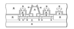
01 GaN Transistor Fabrication Methods
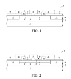
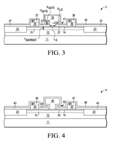
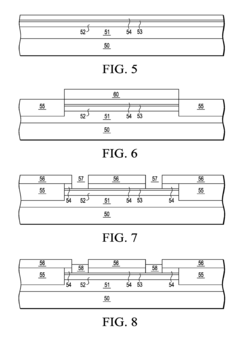
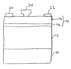
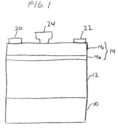
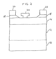
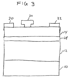
Various methods for fabricating gallium nitride transistors, including epitaxial growth techniques, substrate selection, and processing steps. These methods focus on improving crystal quality, reducing defects, and optimizing the transistor structure for better performance. The fabrication processes often involve specialized growth conditions and post-growth treatments to enhance electrical properties.- GaN transistor fabrication methods: Various methods for fabricating gallium nitride transistors, including epitaxial growth techniques, substrate selection, and processing steps. These methods focus on improving crystal quality, reducing defects, and enhancing device performance. Techniques include MOCVD growth, substrate preparation, and specialized processing to create high-quality GaN layers for transistor applications.
- GaN HEMT device structures: High Electron Mobility Transistor (HEMT) structures based on gallium nitride, featuring specific layer compositions and architectures. These structures typically include AlGaN/GaN heterojunctions that form a two-dimensional electron gas (2DEG) channel. Design innovations focus on improving electron mobility, reducing parasitic effects, and enhancing power handling capabilities through optimized layer structures.
- GaN substrate and crystal growth: Techniques for growing high-quality gallium nitride crystals and substrates for transistor applications. These methods address challenges in producing low-defect GaN materials, including specialized growth conditions, temperature control, and pressure management. Innovations in this area aim to create native GaN substrates with reduced dislocation densities for improved device performance.
- GaN power transistor designs: Specialized gallium nitride transistor designs optimized for power applications, featuring enhanced breakdown voltage, reduced on-resistance, and improved thermal management. These designs incorporate field plates, edge termination structures, and novel gate configurations to handle high voltages and currents while maintaining efficiency. Innovations focus on maximizing the inherent advantages of GaN for power switching applications.
- GaN transistor reliability and performance enhancement: Methods and structures to improve the reliability and performance of gallium nitride transistors, addressing issues such as current collapse, thermal management, and long-term stability. These innovations include surface passivation techniques, buffer layer optimization, and specialized electrode designs to mitigate degradation mechanisms. Approaches focus on extending device lifetime while maintaining the high-performance characteristics of GaN transistors.
02 GaN HEMT Structure and Design
High Electron Mobility Transistor (HEMT) designs using gallium nitride, focusing on the heterostructure layers, gate configurations, and channel engineering. These designs typically include AlGaN/GaN interfaces to create a two-dimensional electron gas (2DEG) with high carrier mobility. Various structural modifications are implemented to enhance power handling, switching speed, and thermal performance.Expand Specific Solutions03 GaN Substrate and Crystal Growth
Techniques for growing high-quality gallium nitride crystals and substrates for transistor applications. These methods address challenges in producing low-defect GaN materials, including specialized growth conditions, buffer layers, and doping strategies. The focus is on creating substrates with uniform properties and minimal lattice mismatch to improve device performance and reliability.Expand Specific Solutions04 GaN Power Transistor Applications
Applications of gallium nitride transistors in power electronics, focusing on high-voltage, high-frequency, and high-temperature operation. These transistors offer advantages over silicon-based devices, including higher breakdown voltage, faster switching speeds, and better thermal conductivity. Specific designs address challenges in power conversion efficiency, reliability under stress conditions, and integration with existing systems.Expand Specific Solutions05 GaN Transistor Performance Enhancement
Methods to enhance the performance of gallium nitride transistors through novel materials, structures, and processing techniques. These enhancements include surface passivation, field plate designs, gate engineering, and thermal management solutions. The focus is on improving key parameters such as breakdown voltage, on-resistance, switching speed, and reliability under various operating conditions.Expand Specific Solutions
Key Industry Players in GaN Semiconductor Market
The Gallium Nitride (GaN) transistor market is experiencing rapid growth, currently in its early maturity phase with significant technological advancements driving adoption. The market is projected to expand substantially due to GaN's superior performance over silicon in high-power applications. Key players form a competitive landscape across multiple regions: established semiconductor giants like Intel, Texas Instruments, and Infineon Technologies lead with extensive resources, while specialized GaN-focused companies such as GaN Systems, Navitas Semiconductor, and Nitronex drive innovation. Academic and research institutions including Xidian University and Peking University contribute to technological advancement. The market shows a collaborative ecosystem where companies are developing proprietary GaN technologies while forming strategic partnerships to accelerate commercialization and address manufacturing challenges.
GaN Systems, Inc.
Technical Solution: GaN Systems specializes in gallium nitride power transistors designed for efficient power conversion applications. Their Island Technology platform features a proprietary cell layout that maximizes current handling capability while minimizing dynamic losses. Their GaN transistors operate at switching frequencies up to 100MHz with power densities 4-5x higher than silicon alternatives. The company's GaNPX packaging technology eliminates wire bonds and provides superior thermal performance, reducing junction-to-case thermal resistance by approximately 50% compared to conventional packages. GaN Systems has developed comprehensive design tools including SPICE models, thermal models, and reference designs to accelerate customer adoption. Their E-mode (enhancement-mode) GaN transistors operate with standard gate drivers, simplifying the transition from silicon to GaN technology for power system designers.
Strengths: Industry-leading power density and switching performance; innovative packaging technology with superior thermal characteristics; comprehensive design ecosystem supporting rapid adoption. Weaknesses: Limited vertical integration compared to larger semiconductor manufacturers; focused primarily on discrete components rather than integrated solutions; higher cost structure than mass-market silicon alternatives.
Analog Devices, Inc.
Technical Solution: Analog Devices has developed a comprehensive GaN technology platform focused on high-performance RF and power applications. Their GaN portfolio includes both discrete transistors and integrated solutions incorporating driver, control, and protection functions. ADI's GaN RF devices operate at frequencies up to 40GHz with power-added efficiencies exceeding 60% in X-band applications, enabling next-generation radar and communication systems. For power applications, ADI has implemented a proprietary GaN-on-Silicon process that achieves breakdown voltages above 650V while maintaining low dynamic RDS(on) characteristics. Their integrated GaN solutions feature advanced gate drive techniques that optimize switching performance while protecting against parasitic turn-on effects. ADI has developed specialized packaging technologies that minimize parasitic inductances, enabling switching speeds exceeding 200V/ns while maintaining electromagnetic compatibility. Their GaN technology has been deployed in applications ranging from 5G infrastructure to industrial motor drives.
Strengths: Extensive signal chain expertise enabling optimized GaN system solutions; strong presence in both RF and power applications; sophisticated packaging and integration capabilities. Weaknesses: Less specialized in GaN compared to pure-play competitors; relatively higher cost structure for some applications; more conservative performance specifications in certain power applications.
Critical Patents and Technical Breakthroughs in GaN Technology
High Speed Gallium Nitride Transistor Devices
PatentActiveUS20150295075A1
Innovation
- A high-frequency, high-voltage gallium nitride field effect transistor device is developed with a thin dielectric passivation layer and gate electrode sidewall extensions spaced apart from the passivation layer, coated with conformal dielectric layers to form a vertical metal-insulator-semiconductor (MIS) sandwich, reducing leakage currents and maintaining high-voltage operation while minimizing capacitance increase.
Homoepitaxial gallium-nitride-based electronic devices and method for producing same
PatentInactiveUS8089097B2
Innovation
- A homoepitaxial GaN-based electronic device is fabricated using a single crystal GaN substrate with a dislocation density less than 10^5 per cm², grown using a supercritical solvent at high temperature and pressure, resulting in high-quality GaN layers with reduced impurities and improved thermal conductivity.
Supply Chain Resilience for GaN Materials
The resilience of the Gallium Nitride (GaN) supply chain has become increasingly critical as the GaN transistor market expands across multiple industries. The primary raw material, gallium, is predominantly obtained as a byproduct of aluminum and zinc processing, creating inherent vulnerabilities in the supply chain. Currently, China dominates global gallium production, accounting for approximately 80% of the world's supply, which introduces geopolitical risks for manufacturers in other regions.
Recent export restrictions and trade tensions have highlighted the fragility of this concentrated supply chain. In response, several strategic initiatives have emerged to enhance supply chain resilience. Material diversification represents one approach, with companies investigating alternative semiconductor materials that can complement or partially substitute GaN in certain applications, including silicon carbide (SiC) and aluminum nitride (AlN).
Geographical diversification of gallium extraction and processing facilities has gained momentum, with investments in Australia, Canada, and Vietnam aimed at establishing alternative supply sources. These efforts are supported by governmental policies in the US, EU, and Japan that provide incentives for domestic semiconductor material production through subsidies and tax benefits under various semiconductor acts and critical minerals strategies.
Recycling and circular economy approaches are showing promise for improving supply chain sustainability. Advanced recycling technologies can recover up to 85% of gallium from end-of-life electronics and manufacturing waste, significantly reducing dependence on primary extraction. Companies like Umicore and Aurubis have developed specialized processes for recovering gallium from production scrap and electronic waste.
Vertical integration strategies are being adopted by major GaN device manufacturers to secure their supply chains. Companies such as Infineon, Qorvo, and Wolfspeed have invested in controlling multiple stages of the value chain, from material sourcing to device fabrication. This approach provides greater visibility and control over potential supply disruptions.
Inventory management practices have evolved in response to recent supply chain shocks. The industry has moved away from just-in-time models toward strategic stockpiling of critical materials, with many manufacturers maintaining 6-12 month reserves of gallium and GaN substrates compared to the previous 2-3 month standards.
Technological innovations in material efficiency are also contributing to supply chain resilience. Advanced epitaxial growth techniques have reduced material waste by up to 40% in GaN wafer production, while thin-film and nanowire approaches allow for significantly reduced material usage while maintaining device performance. These efficiency improvements effectively extend existing gallium supplies and reduce vulnerability to supply disruptions.
Environmental Impact and Sustainability of GaN Manufacturing
The manufacturing processes for Gallium Nitride (GaN) transistors present both environmental challenges and sustainability opportunities that are increasingly influencing market dynamics. Traditional semiconductor manufacturing has historically involved energy-intensive processes and hazardous chemicals, but GaN production introduces specific environmental considerations that merit careful examination.
GaN manufacturing requires significantly less raw material compared to silicon-based alternatives due to the higher power density capabilities of the material. This reduction in material usage translates to lower resource extraction impacts and reduced waste generation throughout the production lifecycle. Additionally, the smaller die sizes of GaN transistors contribute to more efficient use of wafer space, further minimizing resource requirements per functional unit.
Energy consumption during manufacturing remains a critical environmental factor. While GaN production processes are energy-intensive, recent technological innovations have focused on improving energy efficiency in epitaxial growth processes and substrate production. Advanced molecular beam epitaxy (MBE) and metal-organic chemical vapor deposition (MOCVD) techniques have reduced energy requirements by 15-20% over the past five years, according to industry benchmarks.
Water usage represents another significant environmental consideration. GaN manufacturing typically requires ultra-pure water for cleaning and processing steps. Innovative water recycling systems and closed-loop processing techniques have emerged as sustainability solutions, with leading manufacturers reporting water reuse rates exceeding 80% in newer facilities. These improvements directly address water scarcity concerns in semiconductor manufacturing regions.
Chemical management presents both challenges and opportunities for sustainable GaN production. The industry has made substantial progress in replacing certain toxic substances with environmentally preferable alternatives. For instance, newer etching processes have reduced dependence on perfluorinated compounds with high global warming potential. However, certain specialized chemicals remain necessary for achieving the high-performance characteristics of GaN transistors.
End-of-life considerations are increasingly important as the GaN market expands. The durability and longer operational lifetime of GaN devices contribute positively to sustainability by reducing replacement frequency and associated waste. Furthermore, research into GaN recycling technologies has advanced significantly, with pilot programs demonstrating recovery rates of valuable materials exceeding 60%.
Carbon footprint assessments of GaN manufacturing reveal that while production emissions may be higher than conventional silicon in some cases, the lifetime energy savings from GaN device efficiency often result in net environmental benefits. Life cycle analyses indicate that GaN-based power systems can reduce overall carbon emissions by 40-60% compared to silicon alternatives when considering the full product lifecycle.
Unlock deeper insights with Patsnap Eureka Quick Research — get a full tech report to explore trends and direct your research. Try now!
Generate Your Research Report Instantly with AI Agent
Supercharge your innovation with Patsnap Eureka AI Agent Platform!