Gallium Nitride Transistors: Advanced Research in Electrode Efficiency
OCT 14, 20259 MIN READ
Generate Your Research Report Instantly with AI Agent
Patsnap Eureka helps you evaluate technical feasibility & market potential.
GaN Transistor Evolution and Research Objectives
Gallium Nitride (GaN) transistors represent a revolutionary advancement in semiconductor technology, offering significant advantages over traditional silicon-based devices. The evolution of GaN transistor technology began in the early 1990s with fundamental research into wide bandgap semiconductors. This material's exceptional properties, including a bandgap of 3.4 eV compared to silicon's 1.1 eV, enable operation at higher voltages, frequencies, and temperatures while maintaining smaller form factors.
The development trajectory of GaN transistors has been marked by several key milestones. Initial research focused on overcoming material growth challenges, particularly the lack of native substrates. The introduction of Metal-Organic Chemical Vapor Deposition (MOCVD) techniques in the mid-1990s represented a crucial breakthrough, enabling the growth of high-quality GaN epitaxial layers on various substrates. By the early 2000s, researchers had developed the first commercially viable GaN High Electron Mobility Transistors (HEMTs).
Electrode efficiency has emerged as a critical focus area in GaN transistor development. Traditional metal contacts often create performance bottlenecks due to contact resistance issues and thermal management challenges. Recent research has concentrated on novel electrode materials and structures to maximize the inherent advantages of GaN technology. Innovations in this domain aim to reduce parasitic resistances and capacitances while enhancing thermal conductivity at the electrode-semiconductor interface.
The current technical objectives in GaN electrode research encompass several dimensions. First, researchers are pursuing reduced contact resistance through novel metallization schemes and surface treatment techniques. Second, there is significant interest in developing electrode configurations that minimize current crowding effects, which can limit device reliability. Third, thermal management at the electrode level represents a crucial research direction, as GaN devices often operate at power densities that create substantial heat dissipation challenges.
Looking forward, the research roadmap for GaN transistor electrode efficiency includes exploring two-dimensional materials as interfacial layers, developing selective area doping techniques for optimized contact regions, and investigating advanced packaging solutions that integrate cooling mechanisms directly with electrode structures. These efforts align with the broader industry trend toward higher power density and efficiency in power electronics applications.
The ultimate goal of this research is to unlock the full potential of GaN technology by addressing the electrode efficiency bottleneck. Success in this domain could enable widespread adoption of GaN transistors in applications ranging from electric vehicles and renewable energy systems to advanced telecommunications infrastructure and aerospace electronics, potentially revolutionizing multiple industries through superior energy efficiency and performance.
Market Analysis for High-Efficiency Power Electronics
The power electronics market is experiencing a significant transformation driven by the demand for higher efficiency, smaller form factors, and improved thermal performance. Gallium Nitride (GaN) transistors are at the forefront of this revolution, offering substantial advantages over traditional silicon-based technologies. The global power electronics market is projected to reach $49.3 billion by 2027, growing at a CAGR of 5.7% from 2022, with GaN devices representing an increasingly important segment.
Consumer electronics constitutes the largest application sector, accounting for approximately 32% of the market share. The rapid adoption of smartphones, tablets, and other portable devices necessitates more efficient power management solutions, where GaN transistors' superior electrode efficiency provides tangible benefits in terms of reduced power consumption and heat generation.
The automotive sector represents the fastest-growing market segment for high-efficiency power electronics, with a growth rate exceeding 8% annually. The transition toward electric vehicles (EVs) has intensified the need for advanced power conversion technologies. GaN transistors, with their enhanced electrode efficiency, enable more compact and efficient onboard chargers, DC-DC converters, and inverters, directly addressing range anxiety concerns by improving overall vehicle efficiency.
Industrial applications form another substantial market, valued at $10.2 billion in 2022. Factory automation, industrial drives, and uninterruptible power supplies benefit significantly from GaN's higher switching frequencies and reduced switching losses, resulting in smaller passive components and improved system efficiency.
Regionally, Asia-Pacific dominates the high-efficiency power electronics market with a 45% share, driven by the concentration of consumer electronics manufacturing and aggressive EV adoption policies in China, Japan, and South Korea. North America follows with 28% market share, with particular strength in defense and aerospace applications where the radiation hardness of GaN provides additional advantages.
The market dynamics are further influenced by the increasing focus on renewable energy integration. Solar inverters and wind power converters benefit from GaN transistors' ability to operate at higher frequencies, reducing the size and weight of passive components while improving energy harvest efficiency. This segment is growing at 7.3% annually, creating substantial opportunities for advanced electrode designs in GaN transistors.
Pricing trends indicate that while GaN transistors currently command a premium over silicon alternatives, the gap is narrowing as manufacturing volumes increase. Industry analysts predict price parity with silicon MOSFETs in specific power ranges by 2025, which would accelerate adoption across multiple sectors and potentially reshape the competitive landscape of the power electronics industry.
Current Challenges in GaN Electrode Technology
Despite significant advancements in GaN transistor technology, electrode efficiency remains a critical bottleneck limiting overall device performance. Current GaN electrode designs face several interconnected challenges that impede the full realization of GaN's theoretical capabilities. The primary issue involves contact resistance at the metal-semiconductor interface, which typically ranges from 10^-5 to 10^-6 Ω·cm², significantly higher than the ideal values needed for high-frequency and high-power applications.
Surface contamination during fabrication processes presents another substantial challenge. Gallium oxide formation on GaN surfaces creates an insulating layer that degrades electrode performance. Conventional cleaning methods often prove insufficient for complete removal of these oxides, resulting in inconsistent device characteristics across production batches.
Thermal stability constraints further complicate electrode design. During high-power operation, GaN devices can reach temperatures exceeding 200°C, causing metal diffusion, interfacial reactions, and ultimately contact degradation. Traditional electrode materials like Ti/Al/Ni/Au stacks exhibit reliability issues under these thermal conditions, with observed degradation mechanisms including metal migration and void formation at interfaces.
Edge termination effects represent another significant challenge. The electric field crowding at electrode edges leads to premature breakdown and reliability concerns. Current field plate designs provide partial mitigation but introduce additional capacitance that compromises high-frequency performance, creating an engineering trade-off between breakdown voltage and switching speed.
Scalability issues persist in electrode fabrication techniques. While laboratory-scale devices demonstrate promising performance, transferring these results to mass production remains problematic. Techniques like electron beam evaporation provide excellent control but suffer from low throughput, while sputtering offers better production rates but less precise interface control.
The heterogeneous nature of GaN substrates introduces additional complexity. Variations in dislocation density and surface polarity across the wafer result in non-uniform electrode characteristics. This heterogeneity is particularly pronounced at the boundaries between different crystal domains, creating localized regions of high resistance that impact overall device performance.
Recent research has identified current crowding as a significant failure mechanism in GaN electrodes. Under high-current operation, non-uniform current distribution leads to localized heating and accelerated degradation. Simulation studies suggest that optimized electrode geometries could mitigate this effect, but experimental validation remains limited by fabrication constraints and measurement challenges at the microscale level.
State-of-the-Art Electrode Design Solutions
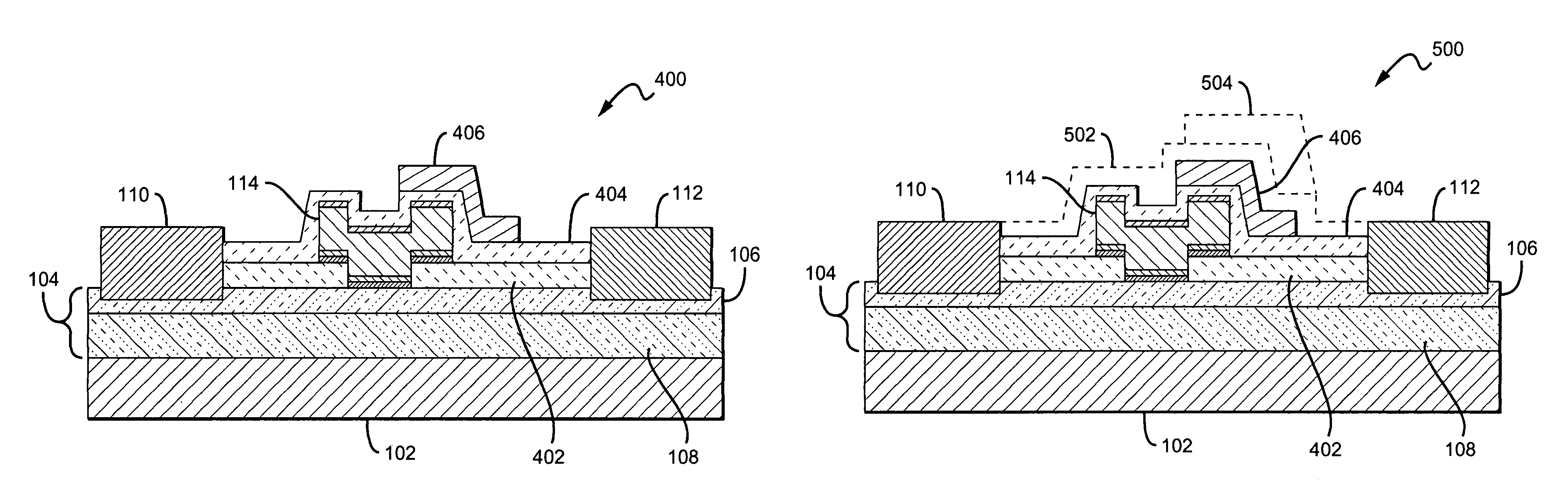
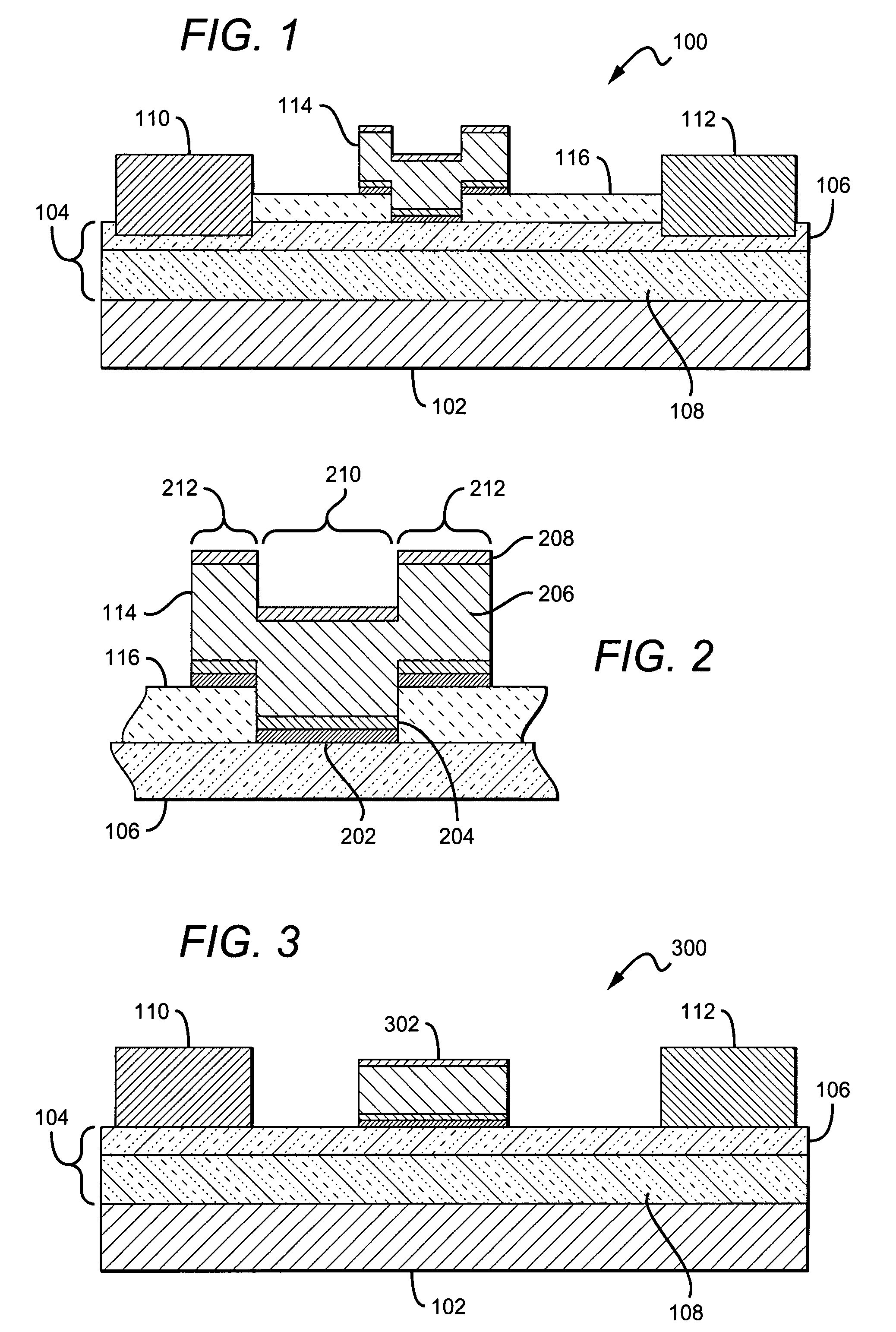
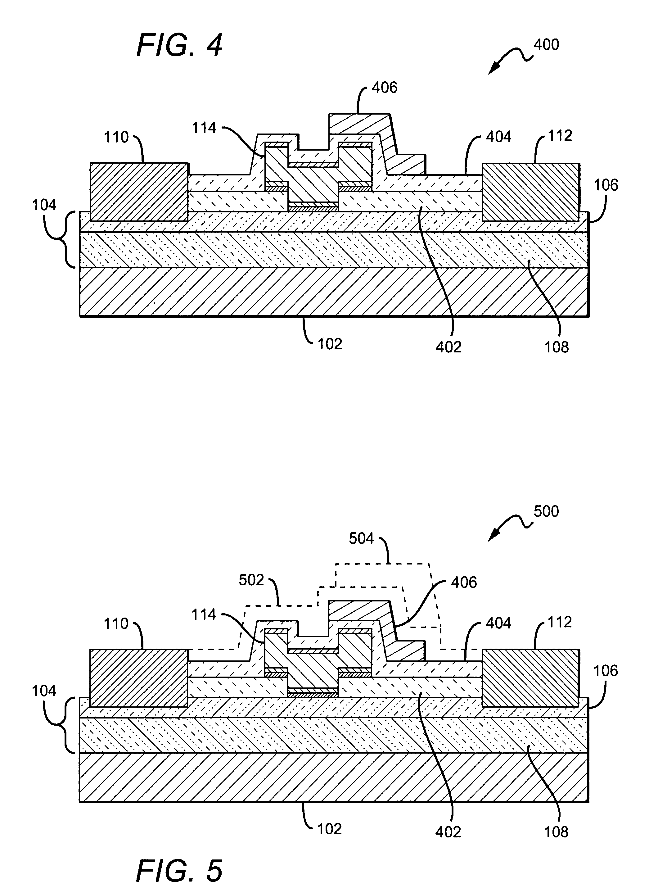
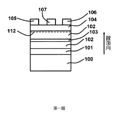
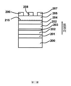
01 Electrode material optimization for GaN transistors
The choice of electrode materials significantly impacts the efficiency of gallium nitride transistors. Using materials with optimal work functions and low contact resistance can enhance electron transport and reduce power losses. Advanced metal stacks, such as Ti/Al/Ni/Au combinations, or novel materials like graphene and metal silicides, have been developed to improve the ohmic contact properties and overall device performance. These optimized electrode materials contribute to higher current densities and improved thermal stability in GaN transistor operations.- Electrode material optimization for GaN transistors: The choice of electrode materials significantly impacts the efficiency of gallium nitride transistors. Using materials with optimal work functions and low contact resistance, such as specific metal alloys or multilayer structures, can enhance electron transport at the electrode-semiconductor interface. Advanced electrode materials can reduce power losses, improve thermal management, and increase overall device efficiency. Proper selection of gate, source, and drain electrode materials is crucial for maximizing the performance advantages of GaN technology.
- Novel electrode structures and fabrication techniques: Innovative electrode structures and fabrication methods can significantly improve GaN transistor efficiency. These include recessed gate structures, field plates, T-shaped gates, and specialized electrode geometries that optimize electric field distribution. Advanced fabrication techniques such as selective area growth, regrowth processes, and precise etching methods enable the creation of these sophisticated electrode structures. These approaches help minimize parasitic resistances and capacitances while enhancing current handling capabilities and switching performance.
- Surface treatment and interface engineering: Surface treatments and interface engineering between electrodes and GaN layers are critical for improving transistor efficiency. Techniques such as plasma treatments, annealing processes, and the use of interfacial layers can reduce defects and traps at the electrode-semiconductor interface. Proper passivation and surface cleaning methods before electrode deposition minimize contact resistance and enhance carrier transport. These approaches lead to improved electrical characteristics, reduced leakage currents, and enhanced overall device reliability and efficiency.
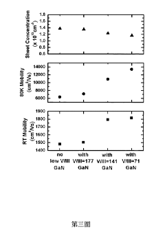
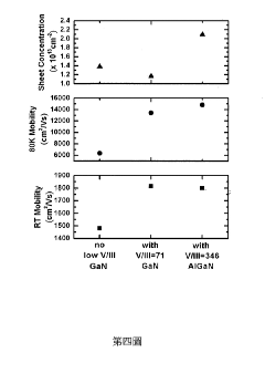
- Heterostructure design for enhanced electrode performance: The design of GaN-based heterostructures significantly impacts electrode efficiency in transistors. Optimized layer structures, including AlGaN/GaN interfaces, buffer layers, and cap layers, can enhance carrier concentration and mobility at the electrode contact regions. Engineering the composition, thickness, and doping profiles of these layers facilitates better charge transfer between electrodes and the active device regions. Advanced heterostructure designs enable higher current densities, lower on-resistance, and improved power handling capabilities.
- Thermal management and reliability enhancement: Thermal management strategies for electrodes are essential for maintaining GaN transistor efficiency during operation. Specialized electrode designs that facilitate heat dissipation, such as integrated heat spreaders or thermally conductive materials, help prevent performance degradation at high power levels. Reliability enhancement techniques, including edge termination structures and field management approaches, protect electrodes from electrical and thermal stress. These methods extend device lifetime while maintaining optimal efficiency under various operating conditions.
02 Electrode structure and geometry design
The physical structure and geometry of electrodes in GaN transistors play a crucial role in device efficiency. Field plate structures, recessed gate designs, and optimized source-drain spacing can effectively manage electric field distribution and reduce parasitic resistances. Innovative electrode geometries help mitigate current crowding effects and enhance heat dissipation. Advanced fabrication techniques allow for precise control of electrode dimensions and profiles, resulting in improved carrier transport efficiency and higher breakdown voltages in high-power applications.Expand Specific Solutions03 Surface treatment and interface engineering
Surface treatments and interface engineering between electrodes and GaN layers significantly impact transistor efficiency. Techniques such as plasma treatment, annealing processes, and surface passivation help reduce interface states and trap densities. The introduction of transition layers or specific dielectric materials can improve carrier injection and extraction at the electrode interfaces. These treatments minimize contact resistance and current leakage, leading to enhanced electron mobility and more efficient device operation under various operating conditions.Expand Specific Solutions04 Novel electrode fabrication techniques
Advanced fabrication techniques for electrodes in GaN transistors have been developed to enhance efficiency. These include selective area growth, regrowth techniques, atomic layer deposition, and advanced lithography methods. Such techniques enable precise control over electrode formation, reducing defects and improving interface quality. Self-aligned processes minimize parasitic capacitances and resistances, while novel deposition methods ensure uniform electrode coverage and adhesion. These fabrication innovations contribute to higher current handling capabilities and improved switching performance.Expand Specific Solutions05 Heterostructure and polarization engineering
Engineering the heterostructure and polarization effects in GaN transistors can significantly improve electrode efficiency. By carefully designing the composition and thickness of barrier layers, the two-dimensional electron gas (2DEG) concentration at the interface can be optimized. Polarization engineering techniques manipulate the built-in electric fields to enhance carrier transport properties. Integration of cap layers and buffer structures further improves the electrode-semiconductor interface characteristics. These approaches result in reduced access resistance and enhanced current flow between the electrodes and the active channel region.Expand Specific Solutions
Leading Companies in GaN Semiconductor Industry
Gallium Nitride (GaN) transistor technology for electrode efficiency is currently in a growth phase, with the market expanding rapidly due to increasing demand for high-power, high-frequency applications. The global GaN power device market is projected to reach significant scale as industries transition from silicon-based technologies. Companies like Wolfspeed, GaN Systems, and Transphorm are leading innovation in this space, while established semiconductor giants including Texas Instruments, Infineon Technologies, and NXP are investing heavily to secure market positions. The technology has reached commercial viability for specific applications but continues to evolve, with research institutions like Xidian University and University of Electronic Science & Technology of China collaborating with industry players to overcome remaining challenges in thermal management, reliability, and cost reduction.
GaN Systems, Inc.
Technical Solution: GaN Systems专注于开发高效率氮化镓晶体管,其核心技术方案围绕Island Technology®专利设计展开。该技术通过优化电极结构,实现了更高的电流密度和更低的导通电阻。公司的GaNPX®封装技术消除了传统引线键合,降低了寄生电感,使晶体管在高频应用中表现出色。在电极效率方面,GaN Systems采用专有的金属化工艺,显著改善了栅极和源极接触电阻,减少了热效应对器件性能的影响。其最新研究表明,优化的电极设计可将开关损耗降低约40%,同时提高功率密度达300W/in³。公司还开发了先进的表面钝化技术,有效抑制了界面陷阱效应,进一步提升了电极效率和器件可靠性。
优势:电极设计显著降低了寄生电感和电阻,使器件在高频应用中具有卓越性能;专有封装技术提供了优异的散热性能,支持更高功率密度。劣势:相比硅基器件,制造成本较高;在某些极端温度条件下,电极可靠性仍需进一步优化;市场渗透率相对较低,尚未实现大规模商业化。
Innoscience Suzhou Semiconductor Co. Ltd.
Technical Solution: Innoscience作为全球最大的8英寸GaN-on-Si晶圆制造商,在氮化镓晶体管电极效率研究方面投入了大量资源。公司的核心技术方案InnoGaN®平台采用创新的电极设计和工艺优化,实现了高效率和高可靠性。Innoscience开发的多层场板结构有效改善了电场分布,提高了器件的击穿电压,同时降低了动态导通电阻。在栅极设计方面,公司采用自对准工艺和优化的金属堆叠结构,显著降低了栅极电阻和寄生电容,提升了器件的开关速度。研究数据表明,其优化的电极结构可将开关损耗降低约25%,同时提高功率密度达3倍。Innoscience还开发了专有的源极和漏极电极工艺,通过优化金属化和退火参数,实现了极低的接触电阻,进一步提升了器件的电流承载能力和效率。
优势:拥有大规模8英寸GaN晶圆生产能力,具有成本优势;电极工艺标准化程度高,产品一致性好;产品覆盖低压到高压全系列应用。劣势:公司成立时间相对较短,产品在市场上的验证时间有限;在高端研究资源和专利积累方面不及部分老牌半导体公司;国际市场渗透率仍需提高。
Critical Patents in GaN Electrode Efficiency
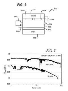
High temperature performance capable gallium nitride transistor
PatentActiveUS8212290B2
Innovation
- The use of a gate electrode made from materials with a high Schottky barrier, such as platinum (Pt), tungsten (W), molybdenum (Mo), chromium (Cr), or nickel-chromium alloys (NiCr), and the incorporation of spacer layers and field plates to reduce peak electric fields and enhance reliability, while maintaining low degradation at high temperatures.
Nitride transistor structure enhances the electron mobility and the carrier concentration of a two-dimensional electron gas channel to achieve efficacy of increasing performance
PatentActiveTW201721865A
Innovation
- Incorporating a nitride intermediate layer with a lower 5-3 ratio between the 2DEG channel and the substrate, using epitaxial growth methods such as MOCVD, to enhance electron mobility and concentration, thereby converting the transistor to an enhancement mode.
Thermal Management Strategies for GaN Devices
Thermal management represents a critical challenge in the development and application of Gallium Nitride (GaN) transistors, particularly when optimizing electrode efficiency. As power densities continue to increase in GaN devices, effective heat dissipation becomes paramount to ensure reliable operation and maximize performance potential.
The inherent material properties of GaN present both advantages and challenges for thermal management. While GaN's wide bandgap allows for higher operating temperatures compared to silicon-based devices, the high power density capabilities mean that localized heating remains a significant concern, especially at the electrode interfaces where current densities are highest.
Several innovative thermal management strategies have emerged to address these challenges. Advanced substrate materials such as silicon carbide (SiC) offer superior thermal conductivity compared to traditional silicon substrates, enabling more efficient heat transfer from the active device regions. Diamond substrates represent the cutting edge in this area, with thermal conductivity approximately five times that of SiC, though manufacturing challenges currently limit widespread adoption.
Electrode design optimization plays a crucial role in thermal management. Novel metallization schemes incorporating heat-spreading layers have demonstrated significant improvements in reducing thermal resistance. Multi-finger electrode configurations distribute heat more effectively across the device area, while advanced metal stacks with optimized thermal interfaces minimize thermal boundary resistance.
Integration of microfluidic cooling channels directly into device packaging represents another promising approach. These structures allow coolant to flow in close proximity to heat-generating regions, dramatically improving thermal extraction capabilities compared to conventional cooling methods. Recent research has demonstrated temperature reductions of up to 30% using such techniques.
Thermal simulation and modeling have become essential tools in the development process. Advanced computational fluid dynamics (CFD) models now incorporate detailed electrode geometries and material interfaces, enabling accurate prediction of thermal hotspots and optimization of cooling strategies before physical prototyping.
Emerging approaches include phase-change materials integrated into packaging to absorb thermal energy during power pulses, and graphene-based thermal interface materials that leverage graphene's exceptional in-plane thermal conductivity. These materials show particular promise for high-frequency GaN applications where thermal cycling is frequent and intense.
The industry continues to move toward holistic thermal management approaches that consider the entire thermal path from junction to ambient, recognizing that electrode efficiency and thermal performance are inextricably linked in next-generation GaN transistor designs.
Environmental Impact and Sustainability Considerations
The environmental impact of Gallium Nitride (GaN) transistor technology extends far beyond its performance advantages, representing a significant shift toward more sustainable semiconductor manufacturing. GaN transistors operate at higher temperatures and voltages than traditional silicon-based alternatives, resulting in substantially improved energy efficiency. This efficiency translates directly to reduced power consumption in end applications, with studies indicating potential energy savings of 10-20% in power conversion systems and up to 40% in certain high-frequency applications.
Manufacturing processes for GaN transistors demonstrate mixed environmental implications. While GaN production requires less water than silicon manufacturing—approximately 30-40% reduction per wafer—it often involves more energy-intensive crystal growth processes. The extraction of gallium, primarily as a byproduct of aluminum and zinc processing, presents fewer direct mining impacts compared to rare earth elements used in other semiconductor technologies.
Life cycle assessments reveal that GaN transistors' environmental advantages become most pronounced during operational phases. The extended operational temperature range (up to 300°C versus silicon's 150°C) results in longer device lifespans and reduced cooling requirements in applications. This characteristic is particularly valuable in power electronics and electric vehicle systems, where thermal management represents a significant sustainability challenge.
Waste management considerations for GaN technologies present both opportunities and challenges. The higher material efficiency of GaN manufacturing produces less waste per functional unit, but end-of-life recycling remains underdeveloped. Current recovery rates for gallium from electronic waste hover below 10%, representing a critical area for improvement as GaN adoption increases.
Recent electrode efficiency improvements in GaN transistors further enhance their sustainability profile. Advanced electrode designs that minimize contact resistance not only improve electrical performance but also reduce operational energy losses by 5-15% compared to earlier GaN implementations. These improvements compound over device lifetimes, significantly reducing carbon footprints in large-scale deployments.
Regulatory frameworks increasingly recognize GaN's sustainability advantages, with the technology receiving favorable classification under various energy efficiency standards worldwide. The European Union's Ecodesign Directive and similar regulations in North America and Asia have begun incorporating considerations that indirectly benefit GaN adoption through performance-based environmental standards.
As research continues to improve electrode efficiency in GaN transistors, the sustainability gap between this technology and conventional alternatives will likely widen, positioning GaN as a cornerstone technology for environmentally responsible electronics in the coming decades.
Unlock deeper insights with Patsnap Eureka Quick Research — get a full tech report to explore trends and direct your research. Try now!
Generate Your Research Report Instantly with AI Agent
Supercharge your innovation with Patsnap Eureka AI Agent Platform!