Gallium Nitride Transistors: Assessment of Electrical Conductivity Improvements
OCT 14, 20259 MIN READ
Generate Your Research Report Instantly with AI Agent
Patsnap Eureka helps you evaluate technical feasibility & market potential.
GaN Transistor Development History and Objectives
Gallium Nitride (GaN) transistor technology has evolved significantly since its inception in the early 1990s. The journey began with the pioneering work of researchers at the University of California, Santa Barbara, who demonstrated the first GaN-based high electron mobility transistor (HEMT) in 1993. This breakthrough laid the foundation for subsequent developments in GaN transistor technology, marking the beginning of a new era in power electronics.
The evolution of GaN transistors has been driven by the inherent material advantages of GaN over traditional silicon. With a bandgap of 3.4 eV compared to silicon's 1.1 eV, GaN offers superior electrical properties, including higher breakdown voltage, faster switching speeds, and reduced on-resistance. These characteristics make GaN transistors particularly suitable for high-power and high-frequency applications, where silicon-based devices face significant limitations.
Throughout the 2000s, significant progress was made in addressing the early challenges of GaN technology, such as current collapse and gate leakage. The introduction of AlGaN/GaN heterostructures and field plates represented critical advancements that substantially improved device performance and reliability. By 2010, commercial GaN transistors began entering the market, primarily targeting RF applications in telecommunications and defense sectors.
The past decade has witnessed accelerated development in GaN transistor technology, with a particular focus on enhancing electrical conductivity. Researchers have explored various approaches, including optimizing the two-dimensional electron gas (2DEG) at the AlGaN/GaN interface, implementing novel buffer layer designs, and developing advanced doping techniques. These efforts have resulted in significant improvements in current density and on-resistance, pushing the boundaries of what GaN transistors can achieve.
The primary objective in GaN transistor development has been to maximize electrical conductivity while maintaining the material's inherent advantages in breakdown voltage and switching speed. This involves addressing the trade-offs between these parameters, as improvements in one often come at the expense of others. Recent research has focused on novel device architectures, such as vertical GaN transistors and hybrid structures, which aim to overcome these limitations and provide a more balanced performance profile.
Looking forward, the technical goals for GaN transistor development include achieving even higher electrical conductivity through innovative material engineering and device design. This encompasses reducing contact resistance, enhancing carrier mobility, and optimizing channel design. Additionally, there is a growing emphasis on improving thermal management and reliability, which are critical factors for widespread adoption in commercial applications.
Market Demand Analysis for High-Conductivity GaN Transistors
The global market for high-conductivity Gallium Nitride (GaN) transistors is experiencing unprecedented growth, driven primarily by the increasing demand for high-power and high-frequency electronic applications. Current market valuations indicate that the GaN power device market is projected to reach $1.1 billion by 2025, with a compound annual growth rate of approximately 22% from 2020 to 2025.
The automotive sector represents one of the most significant market opportunities for high-conductivity GaN transistors. With the rapid expansion of electric vehicles (EVs), there is a growing need for more efficient power conversion systems. GaN transistors with improved electrical conductivity can significantly reduce power losses in EV charging infrastructure and on-board power management systems, extending vehicle range by up to 5-10% compared to silicon-based alternatives.
Telecommunications infrastructure, particularly with the global rollout of 5G networks, constitutes another major market driver. Base stations require high-frequency, high-power amplifiers where GaN transistors excel. Industry reports suggest that GaN-based RF power amplifiers can achieve 15-20% higher efficiency than traditional technologies, translating to substantial energy savings across network deployments.
Consumer electronics manufacturers are increasingly adopting GaN technology for fast-charging solutions. The market for GaN-based chargers grew by 52% in 2022, as consumers demand smaller form factors and faster charging capabilities. Improved conductivity in GaN transistors directly addresses these needs by enabling higher power density in compact designs.
Industrial power systems represent a growing application area where enhanced GaN conductivity provides significant advantages. Factory automation, renewable energy inverters, and data center power supplies all benefit from the higher switching frequencies and reduced power losses that advanced GaN transistors offer. Energy savings of 30-40% have been documented in several industrial applications when replacing silicon-based power devices with GaN alternatives.
Defense and aerospace applications continue to drive premium segment demand for high-performance GaN transistors. Radar systems, electronic warfare equipment, and satellite communications require the exceptional high-frequency performance that only advanced semiconductor materials like GaN can provide.
Market research indicates that customers across all segments are willing to pay a premium of 15-25% for GaN solutions that demonstrate measurable improvements in electrical conductivity, as the operational cost savings and performance benefits outweigh the initial investment. This price elasticity creates significant revenue opportunities for companies that can achieve technological breakthroughs in GaN conductivity enhancement.
Current State and Challenges in GaN Electrical Conductivity
Gallium Nitride (GaN) transistors have emerged as a promising alternative to silicon-based devices due to their superior electrical properties. Currently, GaN technology has achieved significant advancements in power electronics, RF applications, and optoelectronics. The wide bandgap (3.4 eV) and high electron mobility (up to 2000 cm²/Vs) of GaN enable devices to operate at higher frequencies, temperatures, and voltages compared to silicon counterparts.
Despite these advantages, GaN transistors face several critical challenges in electrical conductivity. The primary limitation stems from the lack of native substrates, necessitating heteroepitaxial growth on foreign substrates like sapphire, silicon carbide, or silicon. This mismatch introduces high dislocation densities (10⁶-10¹⁰ cm⁻²) that significantly impair electron transport and reduce overall conductivity performance.
Current-collapse phenomena and dynamic ON-resistance issues represent another major challenge. These reliability concerns manifest as temporary increases in device resistance after high-voltage operation, directly impacting electrical conductivity stability. Research indicates these effects result from electron trapping at surface states and buffer/substrate interfaces, creating depletion regions that restrict current flow.
Contact resistance remains a persistent obstacle in GaN technology. The formation of low-resistance ohmic contacts, particularly to p-type GaN, continues to challenge researchers worldwide. Typical specific contact resistances for n-type GaN range from 10⁻⁵ to 10⁻⁶ Ω·cm², while p-type contacts often exhibit values orders of magnitude higher, limiting overall device performance and efficiency.
Polarization effects inherent to the wurtzite crystal structure of GaN create both opportunities and challenges. While spontaneous and piezoelectric polarization enable the formation of two-dimensional electron gas (2DEG) with high carrier density (>10¹³ cm⁻²) at AlGaN/GaN interfaces, these same effects can cause unpredictable shifts in threshold voltage and conductivity under thermal or mechanical stress.
The global landscape of GaN electrical conductivity research shows concentrated efforts in Japan, the United States, and increasingly China. Japanese institutions like Nagoya University and companies such as Panasonic have pioneered vertical GaN device structures to improve current handling. American entities including MIT, Stanford, and Texas Instruments focus on novel buffer layer designs and surface passivation techniques. European research centers emphasize reliability enhancement through advanced characterization methods.
Material quality inconsistencies across different manufacturing processes present additional challenges. Variations in crystal quality, impurity concentrations, and defect densities directly impact electrical conductivity parameters, making standardization difficult and hindering mass production capabilities for high-performance GaN transistors.
Current Solutions for Enhancing GaN Conductivity
01 Doping techniques to enhance electrical conductivity
Various doping techniques are employed to enhance the electrical conductivity of Gallium Nitride (GaN) transistors. These include the incorporation of specific impurities into the GaN crystal structure to increase carrier concentration. Different dopants can be used to create n-type or p-type regions, which are essential for transistor functionality. The doping concentration and distribution significantly impact the electrical conductivity and overall performance of GaN transistors.- Doping techniques for controlling GaN conductivity: Various doping methods are employed to control the electrical conductivity of gallium nitride (GaN) transistors. These include n-type doping with elements like silicon to increase electron concentration and p-type doping with elements like magnesium to create hole carriers. The doping concentration directly affects the conductivity of the GaN layers, allowing for customization of electrical properties for specific applications. Advanced techniques such as selective area doping and gradient doping profiles enable the creation of optimized device structures with enhanced performance characteristics.
- Two-dimensional electron gas (2DEG) formation in GaN heterostructures: The formation of a two-dimensional electron gas (2DEG) at the interface between GaN and AlGaN layers is crucial for high electron mobility transistors (HEMTs). This 2DEG creates a channel with high carrier concentration and mobility, significantly enhancing electrical conductivity. The sheet carrier density and mobility of the 2DEG can be engineered by adjusting the aluminum content in the AlGaN barrier layer, the layer thickness, and the interface quality. These heterostructures enable transistors with superior high-frequency performance and power handling capabilities compared to conventional semiconductor devices.
- Crystal quality improvement for enhanced conductivity: The electrical conductivity of GaN transistors is significantly influenced by the crystal quality of the semiconductor material. Techniques to reduce defect density, such as dislocations and point defects, are essential for improving carrier mobility and reducing scattering. Advanced growth methods like metal-organic chemical vapor deposition (MOCVD) and molecular beam epitaxy (MBE) with optimized parameters help achieve high-quality GaN crystals. Buffer layer engineering and substrate selection also play crucial roles in minimizing lattice mismatch and associated defects that would otherwise impair electrical conductivity.
- Surface treatment and passivation for conductivity enhancement: Surface treatments and passivation techniques are employed to enhance the electrical conductivity of GaN transistors by reducing surface states and traps. These processes include plasma treatments, chemical cleaning, and deposition of dielectric passivation layers that minimize surface recombination and electron trapping. Proper surface passivation reduces current collapse phenomena and improves dynamic performance by stabilizing the surface potential. Additionally, these treatments can reduce contact resistance at metal-semiconductor interfaces, further enhancing the overall conductivity and performance of GaN transistor devices.
- Polarization engineering for conductivity modulation: Polarization effects in GaN-based materials can be engineered to modulate electrical conductivity in transistor structures. The strong spontaneous and piezoelectric polarization in III-nitride semiconductors creates fixed charges at interfaces, which can be utilized to induce or deplete carriers. By carefully designing layer compositions, thicknesses, and strain states, the polarization fields can be manipulated to enhance channel conductivity. Advanced techniques include the use of polarization-matched interlayers, graded composition regions, and novel heterostructure designs that optimize the distribution of polarization-induced charges for improved device performance.
02 Crystal structure optimization for improved conductivity
The crystal structure of Gallium Nitride plays a crucial role in determining its electrical conductivity properties. Techniques to optimize the crystal structure include reducing defect density, controlling crystal orientation, and improving crystalline quality. Advanced growth methods such as MOCVD and MBE are utilized to achieve high-quality GaN crystals with fewer dislocations and defects, resulting in enhanced electron mobility and electrical conductivity in GaN transistors.Expand Specific Solutions03 Two-dimensional electron gas (2DEG) formation
The formation of a two-dimensional electron gas (2DEG) at the interface between GaN and AlGaN layers significantly enhances the electrical conductivity of GaN transistors. This 2DEG creates a high-mobility channel with high carrier concentration without intentional doping. The thickness ratio and composition of the AlGaN/GaN heterostructure are critical factors that affect the 2DEG density and consequently the electrical conductivity of the transistor channel.Expand Specific Solutions04 Surface treatment and passivation techniques
Surface treatment and passivation techniques are employed to improve the electrical conductivity of GaN transistors by reducing surface states and traps. These techniques include plasma treatments, dielectric deposition, and chemical passivation. Proper surface passivation minimizes current collapse and dispersion effects, leading to more stable and higher conductivity in GaN transistors. The interface quality between GaN and the passivation layer significantly impacts the electrical performance.Expand Specific Solutions05 Contact metallization and ohmic contact formation
The development of low-resistance ohmic contacts is crucial for maximizing the electrical conductivity of GaN transistors. Various metallization schemes and annealing processes are used to create optimal contacts with minimal contact resistance. The selection of appropriate metal stacks and deposition techniques significantly affects the quality of ohmic contacts. Advanced contact technologies enable efficient carrier injection and extraction, enhancing the overall electrical conductivity and performance of GaN transistors.Expand Specific Solutions
Key Industry Players in GaN Semiconductor Market
Gallium Nitride (GaN) transistors are currently in a growth phase, with the market expanding rapidly due to their superior electrical conductivity compared to silicon-based alternatives. The global GaN power device market is projected to reach significant scale, driven by applications in power electronics, RF devices, and automotive sectors. In terms of technological maturity, industry leaders like GaN Systems, Efficient Power Conversion, and Navitas Semiconductor have made substantial advancements in commercializing GaN technology, while established semiconductor companies including Texas Instruments, NXP, Intel, and TSMC are investing heavily in GaN development. Research institutions such as CEA and universities in China are contributing to fundamental improvements in GaN conductivity. The competitive landscape features specialized GaN-focused startups competing against diversified semiconductor giants, with manufacturing capabilities becoming a key differentiator in this rapidly evolving market.
Innoscience Suzhou Semiconductor Co. Ltd.
Technical Solution: Innoscience has developed a unique approach to GaN transistor fabrication using 8-inch silicon wafers, enabling cost-effective mass production while improving electrical conductivity. Their InnoGaN™ technology employs proprietary epitaxial growth techniques that minimize lattice mismatch between GaN and silicon, reducing defect density and improving electron mobility in the 2DEG channel. The company has pioneered advanced gate structures and field plate designs that optimize the electric field distribution throughout the device, allowing for lower on-resistance without compromising breakdown voltage. Their latest generation devices feature sophisticated channel engineering techniques that enhance carrier concentration while maintaining high mobility. Innoscience has achieved industry-leading specific on-resistance values for both low-voltage (80-150V) and high-voltage (650V) GaN transistors, with RDS(on) values as low as 1.2mΩ for 100V devices and 34mΩ for 650V devices in standard packages.
Strengths: Massive manufacturing capacity (over 10,000 wafers per month) enabling economies of scale; comprehensive product portfolio spanning 30V to 650V; excellent price-performance ratio making GaN more accessible. Weaknesses: Less established brand recognition in some markets compared to industry incumbents; relatively newer entrant to high-voltage GaN segment; less extensive application support infrastructure compared to larger semiconductor companies.
GaN Systems, Inc.
Technical Solution: GaN Systems has developed a proprietary Island Technology® die design, combined with GaNPX® packaging and Drive Assist™ technology to significantly improve electrical conductivity in GaN transistors. Their approach uses a unique cell layout that reduces the die resistance by up to 30% compared to conventional designs. The company's GaNPX® packaging eliminates wire bonds and features a near-chipscale footprint with low inductance and thermal resistance, allowing for higher switching frequencies and improved thermal management. Their latest generation devices achieve on-resistance (RDS(on)) values as low as 8mΩ in 100V devices and 50mΩ in 650V devices, representing a significant improvement over silicon-based alternatives. Additionally, their patented embedded cooling technology enables higher current density operation without compromising reliability.
Strengths: Superior power density with up to 4x smaller footprint than competing solutions; excellent thermal performance allowing operation at higher temperatures; significantly lower switching losses enabling higher efficiency systems. Weaknesses: Higher cost compared to silicon alternatives; requires specialized gate drivers; relatively newer technology with less established reliability data compared to silicon MOSFETs.
Critical Patents and Research in GaN Conductivity Enhancement
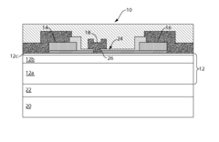
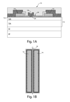
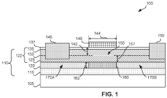
Gallium nitride material transistors and methods associated with the same
PatentInactiveUS7994540B2
Innovation
- The development of gallium nitride material transistors with active regions formed in a gallium nitride layer, integrated with a matching circuit to transform impedance, enabling the amplification of input signals to produce output signals with an adjacent channel power ratio (ACPR) of less than or equal to −20 dBc, while maintaining high drain efficiencies and output powers.
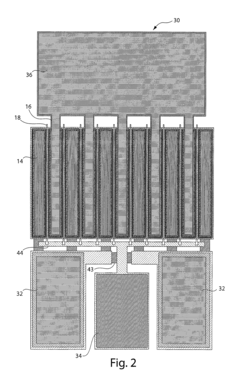
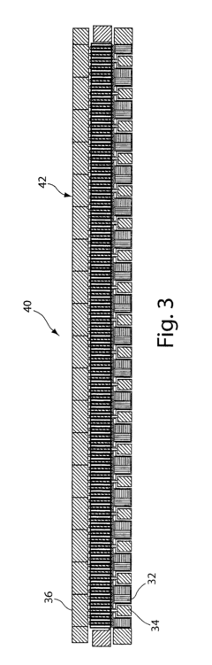
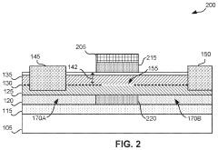
Gallium nitride enhancement mode device
PatentInactiveUS20220093779A1
Innovation
- The fabrication of enhancement mode GaN-based semiconductor devices with a buried p-type region under the two-dimensional electron gas (2DEG) region, allowing for a normally off switching mechanism, achieved by patterning and configuring the p-type material to deplete the 2DEG region and control the threshold voltage, thereby reducing circuit complexity.
Material Science Advancements Supporting GaN Technology
The evolution of Gallium Nitride (GaN) transistor technology has been significantly propelled by concurrent advancements in material science. These developments have been instrumental in addressing the fundamental challenges associated with GaN's electrical conductivity properties, which directly impact transistor performance and efficiency.
Recent breakthroughs in substrate engineering have revolutionized GaN crystal growth techniques. The transition from traditional sapphire substrates to silicon carbide (SiC) and native GaN substrates has dramatically reduced lattice mismatch issues, decreasing defect densities from 10^9 cm^-2 to below 10^6 cm^-2. This reduction in crystallographic defects has directly contributed to improved carrier mobility and reduced scattering, enhancing overall electrical conductivity.
Novel doping methodologies have emerged as another critical advancement area. Precision-controlled silicon doping for n-type conductivity has achieved carrier concentrations exceeding 10^19 cm^-3 while maintaining mobility values above 1000 cm²/V·s. The persistent challenge of effective p-type doping has seen progress through magnesium implantation techniques combined with advanced thermal activation processes, reducing activation energies from 170 meV to approximately 130 meV.
Interface engineering represents another significant material science contribution. The development of specialized AlGaN/GaN heterojunctions with optimized aluminum content (typically 25-30%) has enhanced two-dimensional electron gas (2DEG) formation, achieving sheet carrier densities of 1-2×10^13 cm^-2. These improvements directly translate to higher current densities and lower on-resistance in transistor applications.
Surface passivation technologies have evolved substantially, with silicon nitride and aluminum oxide emerging as superior passivation materials. These advanced dielectrics have reduced surface trap densities by over 70%, minimizing current collapse phenomena and enhancing device reliability under high-field operation conditions.
Thermal management materials have also undergone significant development. Diamond-based heat spreaders with thermal conductivities exceeding 2000 W/m·K have been integrated with GaN devices, enabling more efficient heat dissipation and allowing for higher power density operation without conductivity degradation due to self-heating effects.
The integration of these material science advancements has collectively elevated GaN transistor performance, pushing theoretical limits closer to practical realization. As research continues in areas such as defect engineering and novel heterostructure designs, further improvements in electrical conductivity parameters are anticipated, reinforcing GaN's position as a cornerstone technology for next-generation power electronics and RF applications.
Thermal Management Strategies for High-Power GaN Applications
Effective thermal management is critical for maximizing the performance and reliability of Gallium Nitride (GaN) transistors in high-power applications. As GaN devices operate at higher power densities than traditional silicon-based semiconductors, they generate significant heat that must be efficiently dissipated to maintain optimal electrical conductivity and prevent premature device failure.
The primary thermal management approaches for high-power GaN applications include advanced packaging technologies that utilize materials with superior thermal conductivity. Diamond-based composite substrates have emerged as promising solutions, offering thermal conductivity values exceeding 1500 W/mK compared to conventional silicon carbide substrates (approximately 370 W/mK). These materials significantly enhance heat dissipation pathways from the active device region.
Active cooling techniques represent another crucial strategy for thermal management in GaN transistors. Microfluidic cooling channels integrated directly into device packages can remove heat more efficiently than traditional air cooling methods. Recent research demonstrates that such liquid cooling systems can reduce junction temperatures by up to 40°C under high-power operation conditions, directly improving electrical conductivity by reducing phonon scattering effects in the semiconductor material.
Thermal interface materials (TIMs) play a vital role in the thermal management stack. Novel carbon nanotube-based TIMs and graphene-enhanced thermal greases have demonstrated thermal resistances below 5 mm²K/W, representing a significant improvement over conventional materials. These advanced TIMs minimize thermal boundary resistance between the GaN device and heat sink, enabling more efficient heat transfer across interfaces.
Innovative heat spreading techniques using embedded vapor chambers have shown promising results for managing thermal hotspots in GaN power amplifiers. These solutions distribute heat more uniformly across larger surface areas, preventing localized overheating that can degrade electrical performance. Experimental data indicates that such approaches can maintain temperature gradients below 5°C across the active device area even at power densities exceeding 40 W/mm².
Computational fluid dynamics (CFD) modeling has become essential for optimizing thermal management solutions for specific GaN applications. Advanced simulation tools now incorporate electro-thermal coupling effects, allowing designers to predict how temperature distributions affect electrical conductivity parameters with greater accuracy. These models enable the development of application-specific cooling solutions that maximize electrical performance while ensuring long-term reliability.
Unlock deeper insights with Patsnap Eureka Quick Research — get a full tech report to explore trends and direct your research. Try now!
Generate Your Research Report Instantly with AI Agent
Supercharge your innovation with Patsnap Eureka AI Agent Platform!