Gallium Nitride Transistor Development and Compliance with International Standards
OCT 14, 202510 MIN READ
Generate Your Research Report Instantly with AI Agent
Patsnap Eureka helps you evaluate technical feasibility & market potential.
GaN Transistor Evolution and Development Objectives
Gallium Nitride (GaN) transistor technology has evolved significantly since its inception in the early 1990s, marking a revolutionary advancement in semiconductor materials beyond traditional silicon. The journey began with rudimentary research into wide bandgap semiconductors, with GaN emerging as a promising candidate due to its exceptional electron mobility and breakdown voltage characteristics. By the late 1990s, researchers had successfully demonstrated the first functional GaN High Electron Mobility Transistors (HEMTs), setting the foundation for future development.
The early 2000s witnessed critical breakthroughs in epitaxial growth techniques, particularly Metal-Organic Chemical Vapor Deposition (MOCVD), which enabled the production of high-quality GaN layers on various substrates. This period also saw significant advancements in device architecture, with the introduction of field plates and improved gate designs that substantially enhanced performance metrics. The evolution continued with the commercialization of the first GaN RF devices around 2005, primarily targeting defense and telecommunications applications.
From 2010 onwards, GaN transistor technology expanded into power electronics, driven by the increasing demand for higher efficiency and power density in energy conversion systems. This transition was facilitated by improvements in substrate technology, particularly the development of GaN-on-Silicon, which dramatically reduced production costs while maintaining performance advantages. Concurrently, enhanced passivation techniques and surface treatment methods addressed reliability concerns, enabling broader commercial adoption.
The current technological trajectory aims to further optimize GaN transistor performance across multiple parameters. Key objectives include increasing the maximum operating frequency beyond 300 GHz for RF applications, enhancing power handling capabilities to exceed 10 kW/cm², and improving thermal management to allow operation at junction temperatures above 250°C. Additionally, there is a focused effort to reduce on-resistance below 1 mΩ·cm² for power devices, which would represent a significant advantage over silicon-based alternatives.
International standardization represents another critical development objective, with organizations such as JEDEC, IEC, and IEEE working to establish unified testing protocols and reliability standards specific to GaN technology. These standards aim to address the unique characteristics of GaN devices, including dynamic on-resistance, current collapse phenomena, and long-term reliability under various operating conditions. Compliance with these emerging standards is becoming increasingly important for market acceptance and regulatory approval.
Looking forward, the GaN transistor development roadmap emphasizes several key goals: achieving monolithic integration with control and protection circuitry, developing normally-off (enhancement-mode) devices with improved threshold voltage stability, and creating vertical GaN structures capable of handling ultra-high voltage applications exceeding 1200V. These advancements will be essential to enable GaN technology's expansion into emerging markets such as electric vehicles, renewable energy systems, and next-generation communication infrastructure.
Market Analysis for GaN Power Electronics
The global market for Gallium Nitride (GaN) power electronics has experienced remarkable growth in recent years, driven by increasing demand for high-efficiency power conversion systems across multiple industries. Current market valuations place the GaN power device sector at approximately 1.4 billion USD in 2023, with projections indicating a compound annual growth rate (CAGR) of 25% through 2028, potentially reaching 4.3 billion USD by the end of this forecast period.
Consumer electronics represents the largest application segment, accounting for roughly 32% of the total market share. This dominance stems from the integration of GaN transistors in fast chargers, wireless charging systems, and power adapters, where their superior efficiency and smaller form factors provide significant competitive advantages over traditional silicon-based solutions.
The automotive sector follows closely as the second-largest market segment, currently representing 28% of GaN power electronics applications. With the accelerating transition toward electric vehicles (EVs), demand for GaN-based power conversion systems in onboard chargers, DC-DC converters, and traction inverters has intensified. Industry analysts predict this segment will overtake consumer electronics by 2026, as automotive manufacturers increasingly adopt GaN technology to improve vehicle range and charging efficiency.
Industrial applications constitute approximately 22% of the market, with significant implementation in motor drives, industrial power supplies, and renewable energy systems. The telecommunications sector accounts for 15% of market share, primarily utilizing GaN in base station power amplifiers and data center power delivery systems.
Regionally, Asia-Pacific dominates the GaN power electronics market with 45% share, driven by strong manufacturing capabilities in Japan, South Korea, Taiwan, and China. North America follows at 30%, with Europe representing 20% of the global market. The remaining 5% is distributed across other regions, though Middle Eastern and African markets are showing accelerated adoption rates.
Key market drivers include the growing emphasis on energy efficiency regulations worldwide, miniaturization trends in electronics, and the expanding electric vehicle ecosystem. The superior performance characteristics of GaN transistors—including higher switching frequencies, reduced power losses, and improved thermal management—position them favorably against silicon carbide (SiC) and traditional silicon technologies in applications requiring high power density.
Market challenges include relatively higher production costs compared to silicon alternatives, supply chain constraints for high-quality GaN substrates, and the need for specialized design expertise. Additionally, compliance with evolving international standards presents both challenges and opportunities for market participants as regulatory frameworks continue to develop around this emerging technology.
Technical Barriers and Global GaN Development Status
Despite significant advancements in Gallium Nitride (GaN) transistor technology, several technical barriers continue to impede its widespread adoption and standardization. Material quality remains a primary challenge, with defect densities in GaN substrates still higher than those in silicon, leading to reliability concerns and performance limitations. These defects, including threading dislocations and point defects, can significantly impact device performance and longevity, particularly in high-power applications.
Thermal management presents another substantial hurdle. GaN devices generate significant heat during operation due to their high-power density capabilities. Current packaging technologies struggle to efficiently dissipate this heat, limiting the full potential of GaN transistors in high-performance applications. This challenge is particularly pronounced in compact designs where thermal solutions must be increasingly sophisticated.
Dynamic Ron effects and current collapse phenomena continue to plague GaN transistor performance, especially in high-voltage switching applications. These reliability issues stem from charge trapping mechanisms that are not fully understood or controlled in current manufacturing processes, creating inconsistencies in device behavior under varying operational conditions.
Globally, GaN development shows distinct regional characteristics. The United States leads in defense and aerospace applications, with significant investment from both government agencies and private corporations. Japan maintains strength in optoelectronics and high-frequency GaN applications, while South Korea focuses on consumer electronics integration. Europe has established a robust ecosystem for automotive and industrial applications, particularly in Germany and France.
China has rapidly expanded its GaN research and production capabilities, particularly in telecommunications infrastructure, though gaps remain in advanced manufacturing techniques. Taiwan leverages its semiconductor manufacturing expertise to position itself as a key player in GaN production scaling.
Standardization efforts vary significantly across regions. The IEEE in North America, IEC in Europe, and various national standards bodies in Asia have developed different approaches to GaN transistor specifications. This fragmentation creates compliance challenges for manufacturers targeting global markets, as devices must meet multiple, sometimes conflicting requirements.
The lack of unified testing protocols for reliability assessment further complicates international standardization efforts. Different regions emphasize different performance parameters and reliability metrics, making cross-market certification processes complex and costly for manufacturers seeking global distribution of their GaN products.
Current GaN Transistor Design Architectures
01 GaN transistor fabrication methods
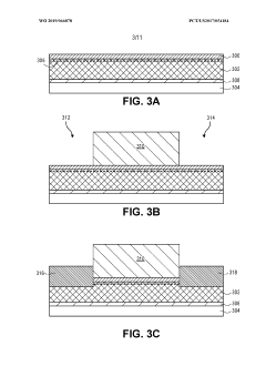
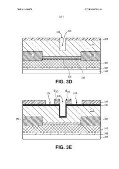
Various methods for fabricating gallium nitride transistors, including epitaxial growth techniques, substrate preparation, and device structure formation. These methods focus on improving the quality of GaN layers, reducing defects, and enhancing overall device performance. Specific techniques include MOCVD growth, substrate engineering, and specialized layer structures to optimize transistor characteristics.- Fabrication methods for GaN transistors: Various methods for fabricating gallium nitride transistors have been developed to improve performance and reliability. These methods include specific growth techniques for GaN layers, substrate preparation processes, and specialized etching procedures. The fabrication processes often focus on reducing defects in the crystal structure and improving the interface quality between different layers, which directly impacts the transistor's electrical characteristics and operational stability.
- GaN transistor structural designs: Different structural designs for gallium nitride transistors have been developed to enhance performance characteristics. These designs include various gate configurations, channel structures, and layer arrangements. Innovations in transistor architecture focus on improving parameters such as breakdown voltage, on-resistance, switching speed, and thermal management. Advanced structural designs often incorporate features like field plates, recessed gates, or specialized buffer layers to optimize device performance.
- GaN substrate and epitaxial growth technology: The quality of gallium nitride substrates and epitaxial layers is crucial for high-performance transistors. Technologies have been developed for growing high-quality GaN crystals, reducing defect density, and controlling doping profiles. Methods include MOCVD (Metal Organic Chemical Vapor Deposition), HVPE (Hydride Vapor Phase Epitaxy), and MBE (Molecular Beam Epitaxy) techniques. Innovations in this area focus on achieving uniform, defect-free layers with precise thickness and composition control.
- High-frequency and power GaN transistor applications: Gallium nitride transistors are particularly valuable for high-frequency and high-power applications due to their wide bandgap properties. Specialized designs have been developed for RF amplifiers, power converters, and high-temperature electronics. These applications leverage GaN's ability to operate at higher voltages, frequencies, and temperatures compared to silicon-based devices. Innovations focus on optimizing parameters such as power density, efficiency, linearity, and reliability under extreme operating conditions.
- GaN transistor enhancement techniques: Various techniques have been developed to enhance the performance of gallium nitride transistors. These include surface passivation methods, novel contact materials, and specialized doping profiles. Enhancement techniques focus on reducing parasitic resistances, improving carrier mobility, minimizing leakage currents, and enhancing thermal dissipation. Advanced approaches may incorporate heterojunctions, quantum wells, or novel dielectric materials to achieve superior electrical characteristics and reliability.
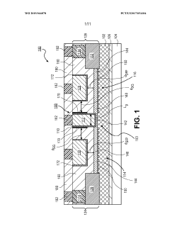
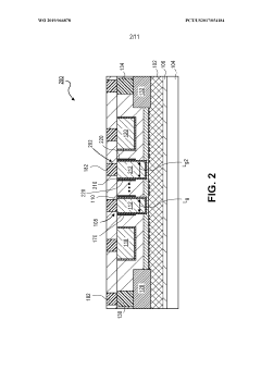
02 High electron mobility transistor (HEMT) structures
Design and implementation of GaN-based high electron mobility transistors (HEMTs), which utilize the two-dimensional electron gas (2DEG) formed at the interface between GaN and AlGaN layers. These structures feature high electron mobility, high breakdown voltage, and excellent high-frequency performance. Various approaches to enhance the 2DEG formation, reduce parasitic effects, and improve thermal management are included.Expand Specific Solutions03 GaN substrate and crystal growth technologies
Technologies related to the growth of high-quality gallium nitride crystals and substrates for transistor applications. This includes methods for reducing dislocation density, controlling crystal orientation, and producing larger substrate sizes. Various approaches such as hydride vapor phase epitaxy (HVPE), ammonothermal growth, and defect reduction techniques are employed to create substrates suitable for high-performance GaN transistors.Expand Specific Solutions04 Power and RF GaN transistor designs
Specialized designs for gallium nitride transistors targeting power electronics and radio frequency (RF) applications. These designs focus on high breakdown voltage, low on-resistance, high current density, and efficient heat dissipation. Various gate structures, field plates, passivation techniques, and packaging solutions are employed to maximize performance in high-power and high-frequency applications.Expand Specific Solutions05 GaN heterostructure and interface engineering
Engineering of heterostructures and interfaces in gallium nitride transistors to enhance performance characteristics. This includes the development of novel buffer layers, barrier layers, cap layers, and interface treatments to improve carrier transport, reduce leakage currents, and enhance reliability. Various material combinations and layer sequences are explored to optimize the electronic properties at critical interfaces within the transistor structure.Expand Specific Solutions
Leading GaN Semiconductor Manufacturers and Competitors
The Gallium Nitride (GaN) transistor market is currently in a growth phase, characterized by increasing adoption across power electronics, RF applications, and telecommunications. The global market is projected to reach significant scale, driven by demand for high-efficiency power conversion and high-frequency performance. Leading players demonstrate varying levels of technological maturity: Wolfspeed, Efficient Power Conversion, and GaN Systems have established commercial product lines, while Intel, NXP, and Infineon are leveraging their semiconductor expertise to advance GaN integration. Asian manufacturers like Huawei, TSMC, and Silan are rapidly developing capabilities, particularly in epitaxial growth and device fabrication. Research institutions including Arizona State University and North Carolina State University continue to push fundamental innovations, while compliance with international standards remains a critical focus area for market expansion.
Analog Devices, Inc.
Technical Solution: Analog Devices has developed a specialized GaN transistor platform targeting precision RF and mixed-signal applications. Their approach focuses on integrating GaN power devices with advanced analog circuitry to create complete signal chain solutions. ADI's GaN technology features proprietary epitaxial layer structures that minimize charge trapping effects, resulting in superior linearity performance critical for communications infrastructure. Their manufacturing process incorporates advanced thermal management techniques including through-substrate vias and copper-filled thermal pathways that reduce junction-to-case thermal resistance to below 0.5°C/W[9]. ADI has established comprehensive qualification procedures that address both commercial and defense standards, including MIL-PRF-38534 for high-reliability applications. Their GaN devices demonstrate exceptional ruggedness with survival capabilities under 10:1 VSWR conditions at full rated power. ADI has pioneered integrated power management and protection features within their GaN solutions, including on-chip temperature sensing and current limiting functionality[10]. Their compliance framework includes extensive electromagnetic compatibility testing to ensure their GaN solutions meet global regulatory requirements.
Strengths: Superior integration capabilities combining GaN with precision analog; excellent linearity performance for communications applications; comprehensive qualification for both commercial and defense standards. Weaknesses: More focused on specialized applications rather than high-volume power conversion; higher cost structure compared to pure-play power semiconductor companies; limited voltage ratings compared to power-focused competitors.
Wolfspeed, Inc.
Technical Solution: Wolfspeed has pioneered vertical GaN transistor technology with their proprietary CAVET (Current Aperture Vertical Electron Transistor) architecture that enables higher breakdown voltages and current densities than lateral devices. Their technology incorporates advanced epitaxial growth techniques to minimize defect densities and optimize carrier mobility. Wolfspeed's GaN-on-SiC platform delivers superior thermal conductivity (>3.5 W/cm·K) compared to GaN-on-Si alternatives, enabling higher power density applications[1]. Their compliance strategy includes comprehensive reliability testing protocols that exceed JEDEC standards, with devices demonstrating MTTF (Mean Time To Failure) exceeding 10^7 hours at 175°C junction temperatures[3]. Wolfspeed has also developed specialized passivation techniques to mitigate surface-related degradation mechanisms common in GaN HEMTs.
Strengths: Industry-leading thermal performance with SiC substrates; vertical device architecture enables higher voltage operation; established reliability testing framework exceeding international standards. Weaknesses: Higher manufacturing costs compared to silicon-based alternatives; limited economies of scale compared to silicon manufacturing; challenges in achieving full compatibility with existing silicon manufacturing infrastructure.
Critical Patents and Innovations in GaN Technology
Gallium nitride high electron mobility transistor
PatentInactiveUS20230411509A1
Innovation
- Incorporating p-type gallium nitride islands between the gate and drain electrodes, which act as electrically floating islands to recombine redundant electrons on the barrier layer, thereby maintaining the concentration of two-dimensional electron gas and enhancing the transistor's reliability.
Gallium nitride transistors with source and drain field plates and their methods of fabrication
PatentWO2019066878A1
Innovation
- Incorporating source and drain field plates in GaN transistors, which are biased independently of the gate voltage, allows for improved control of the drain field distribution, increasing breakdown voltage and linearity by adjusting the distance of the field plates from the respective regions.
International Standards Compliance Framework
The international standards landscape for Gallium Nitride (GaN) transistors is complex and multifaceted, requiring manufacturers to navigate various regulatory frameworks across different regions. The International Electrotechnical Commission (IEC) has established several standards specifically addressing wide bandgap semiconductors, including IEC 63068 which covers reliability assessment methods for GaN power conversion devices. This standard provides crucial guidelines for testing procedures and reliability metrics that GaN transistors must meet.
In the United States, the JEDEC Solid State Technology Association has developed JEP180 and JEP173 standards which outline specific guidelines for GaN power devices, including reliability testing methodologies and qualification requirements. These standards have become increasingly important as GaN transistors transition from military and specialized applications to mainstream commercial markets.
The European Union's regulatory framework includes compliance with the RoHS (Restriction of Hazardous Substances) Directive and the REACH (Registration, Evaluation, Authorization and Restriction of Chemicals) regulation, which impact the materials and manufacturing processes used in GaN transistor production. Additionally, the EU's Ecodesign Directive increasingly influences power efficiency requirements that favor GaN technology's superior performance characteristics.
In Asia, Japan's JEITA (Japan Electronics and Information Technology Industries Association) and China's GB standards have established region-specific requirements for semiconductor devices, including emerging provisions for GaN transistors. These standards often focus on quality control, reliability testing, and environmental considerations specific to local manufacturing conditions.
Safety certification bodies such as UL (Underwriters Laboratories) and TÜV have developed specialized testing protocols for GaN-based power systems, addressing the unique characteristics of these devices compared to traditional silicon-based components. These certifications are becoming increasingly mandatory for market access in many regions.
Electromagnetic compatibility (EMC) standards, including IEC 61000 series and CISPR requirements, present unique challenges for GaN transistors due to their faster switching speeds and potential for higher electromagnetic interference. Manufacturers must design GaN systems with careful consideration of EMC compliance from early development stages.
The automotive industry has particularly stringent requirements outlined in the AEC-Q101 qualification for discrete semiconductors, which has been adapted to address the specific characteristics of GaN transistors. As GaN technology increasingly penetrates automotive applications, compliance with these standards becomes critical for market acceptance.
Harmonization efforts between different standards bodies are ongoing, with organizations like the International Standards Organization (ISO) working to create more unified approaches to GaN semiconductor qualification and testing methodologies, potentially simplifying the compliance landscape for manufacturers in the coming years.
Thermal Management Solutions for GaN Devices
Thermal management represents a critical challenge in the development and deployment of Gallium Nitride (GaN) transistors. Due to their high power density and operating frequencies, GaN devices generate significant heat that must be efficiently dissipated to maintain performance and reliability. Current thermal management solutions for GaN devices can be categorized into several approaches, each with distinct advantages and limitations.
Advanced packaging technologies have emerged as a primary thermal management strategy. Flip-chip configurations, where the active device surface faces the substrate, provide shorter thermal paths compared to traditional wire-bonded packages. Diamond-copper composite substrates offer thermal conductivity up to 3-5 times higher than conventional materials, significantly enhancing heat dissipation capabilities.
Integrated cooling solutions represent another innovative approach. Microfluidic cooling channels directly integrated into device packages can remove heat at the source, achieving thermal resistances below 0.1 K/W. These systems utilize specialized coolants with high thermal capacity circulating through microscale channels fabricated within the device substrate or package.
Novel material interfaces have also shown promising results. Thermal interface materials (TIMs) incorporating graphene, carbon nanotubes, or metal-matrix composites demonstrate thermal conductivities exceeding 25 W/m·K, substantially reducing thermal boundary resistance between device layers and heat sinks.
Computational fluid dynamics (CFD) modeling has become essential for optimizing thermal management solutions. Advanced simulation tools now incorporate multi-physics capabilities that simultaneously model electrical, thermal, and mechanical behaviors of GaN devices, enabling more accurate prediction of hotspots and thermal gradients under various operating conditions.
Industry standards for thermal management of GaN devices continue to evolve. JEDEC JEP180 and IEC 60747-9 provide guidelines for thermal characterization and measurement techniques specific to wide-bandgap semiconductors. Compliance with these standards ensures consistent thermal performance evaluation across different manufacturers and applications.
Recent advancements include phase-change cooling systems that utilize the latent heat of vaporization to achieve cooling capacities exceeding 500 W/cm². These systems are particularly effective for high-power RF and power conversion applications where transient thermal loads can be significant. Additionally, three-dimensional heat spreading structures using conformal vapor chamber technology have demonstrated the ability to reduce peak temperatures by up to 40% compared to conventional cooling methods.
Unlock deeper insights with Patsnap Eureka Quick Research — get a full tech report to explore trends and direct your research. Try now!
Generate Your Research Report Instantly with AI Agent
Supercharge your innovation with Patsnap Eureka AI Agent Platform!