Why Gallium Nitride Transistors are Preferred in High-Frequency Electronics
OCT 14, 202510 MIN READ
Generate Your Research Report Instantly with AI Agent
Patsnap Eureka helps you evaluate technical feasibility & market potential.
GaN Technology Background and Objectives
Gallium Nitride (GaN) technology represents a revolutionary advancement in semiconductor materials that has transformed high-frequency electronics over the past two decades. Initially developed in the 1990s, GaN has emerged as a superior alternative to traditional silicon-based semiconductors for high-power, high-frequency applications. The wide bandgap properties of GaN (3.4 eV compared to silicon's 1.1 eV) enable it to withstand significantly higher electric fields and operate at elevated temperatures, making it particularly valuable for demanding electronic environments.
The evolution of GaN technology has been marked by continuous improvements in material quality, device design, and manufacturing processes. Early research focused primarily on addressing fundamental material challenges, such as reducing defect densities and developing suitable substrates. As these issues were gradually resolved, attention shifted toward optimizing device structures and enhancing performance characteristics, including power density, efficiency, and reliability.
Market demands for more efficient power conversion, higher data transmission rates, and more compact electronic systems have been key drivers behind GaN technology development. The increasing need for energy-efficient power electronics in automotive, renewable energy, and data center applications has further accelerated GaN adoption. Additionally, the expansion of 5G networks and advanced radar systems has created substantial demand for high-frequency GaN devices capable of operating in the millimeter-wave spectrum.
The primary technical objectives for GaN technology development include improving power density to enable more compact and efficient systems, enhancing thermal management capabilities to ensure reliable operation under extreme conditions, and reducing manufacturing costs to facilitate broader commercial adoption. Researchers are also focused on extending the frequency range of GaN devices into the terahertz domain, which would unlock new applications in sensing, imaging, and communications.
Current research efforts are concentrated on several fronts: developing vertical GaN device architectures for ultra-high-voltage applications, integrating GaN with complementary materials like silicon carbide to leverage the advantages of both, and creating novel packaging solutions that can effectively dissipate heat from increasingly power-dense chips. There is also significant work being done to improve the reliability and lifetime of GaN devices, particularly under high-stress operating conditions.
The trajectory of GaN technology suggests continued expansion into new application domains as performance improves and costs decrease. With ongoing advancements in epitaxial growth techniques, device fabrication processes, and circuit design methodologies, GaN is positioned to become the dominant semiconductor technology for high-frequency electronics in the coming decade, potentially displacing silicon in numerous applications where performance requirements exceed silicon's fundamental limitations.
Market Demand Analysis for High-Frequency Electronics
The high-frequency electronics market has experienced substantial growth driven by increasing demand for faster data transmission, improved power efficiency, and miniaturization across multiple industries. The global high-frequency electronics market was valued at approximately 42.8 billion USD in 2022 and is projected to reach 69.3 billion USD by 2028, growing at a CAGR of 8.4% during the forecast period.
Telecommunications represents the largest market segment, with 5G infrastructure deployment creating unprecedented demand for high-frequency components capable of operating efficiently in the 24-100 GHz range. Network providers are investing heavily in equipment that can support wider bandwidths and higher data rates, making GaN transistors particularly attractive due to their superior performance at these frequencies.
The defense and aerospace sectors constitute another significant market, with military radar systems, electronic warfare equipment, and satellite communications requiring components that can deliver high power at high frequencies while maintaining reliability in harsh environments. The defense electronics market alone is expected to grow at 4.6% annually through 2027, with a substantial portion dedicated to high-frequency applications where GaN excels.
Consumer electronics represents a rapidly expanding application area, particularly with the proliferation of wireless charging technologies, high-speed Wi-Fi routers, and IoT devices. The consumer demand for faster wireless connections and more efficient power management is driving adoption of advanced semiconductor technologies like GaN.
Industrial applications, including industrial automation, medical equipment, and scientific instrumentation, are increasingly requiring high-frequency components for improved precision and performance. The industrial IoT market is expected to reach 106.1 billion USD by 2026, with communication components being a key growth segment.
Automotive electronics represents an emerging market for high-frequency components, particularly with the advancement of autonomous driving technologies, vehicle-to-everything (V2X) communications, and advanced driver assistance systems. The automotive radar market alone is projected to grow at 11.7% annually, creating significant opportunities for GaN technology.
Regional analysis indicates that North America and Asia-Pacific dominate the high-frequency electronics market, with China, Japan, South Korea, and Taiwan being major manufacturing hubs. Europe follows closely, with significant research and development activities in countries like Germany and France.
Market challenges include high initial costs of GaN technology compared to silicon alternatives, though this gap is narrowing as manufacturing scales up. Supply chain constraints and geopolitical factors affecting rare earth materials also present potential market limitations that industry players must navigate.
Current State and Challenges of GaN Transistors
Gallium Nitride (GaN) transistors have emerged as a revolutionary technology in high-frequency electronics, offering significant advantages over traditional silicon-based devices. Currently, GaN transistors are being widely adopted in various applications including telecommunications, radar systems, satellite communications, and power electronics due to their superior performance characteristics.
The global market for GaN power devices is experiencing rapid growth, with projections indicating a compound annual growth rate (CAGR) of approximately 22% from 2021 to 2026. This growth is primarily driven by increasing demand for high-frequency applications in 5G infrastructure, defense systems, and electric vehicles. Major semiconductor manufacturers have significantly increased their investments in GaN technology development and production capacity expansion.
Despite the promising advancements, GaN transistor technology faces several critical challenges. The most significant technical hurdle remains the "current collapse" phenomenon, where device performance degrades under high-voltage switching conditions due to electron trapping effects. This issue particularly impacts reliability in power conversion applications and requires sophisticated passivation techniques and buffer layer designs to mitigate.
Thermal management presents another substantial challenge. GaN devices generate significant heat during operation at high frequencies and power densities. Current cooling solutions often prove inadequate for maintaining optimal operating temperatures, necessitating advanced thermal management strategies including novel packaging technologies and integration of diamond heat spreaders.
Cost factors continue to constrain widespread adoption. The manufacturing processes for GaN transistors remain more expensive than silicon alternatives, with substrate costs being particularly prohibitive. While silicon carbide (SiC) substrates offer better thermal performance, they significantly increase production expenses. The industry is actively pursuing cost reduction through economies of scale and development of GaN-on-silicon technology.
Reliability and standardization issues persist as barriers to broader implementation. Long-term reliability data remains limited compared to mature silicon technologies, creating hesitation among conservative industries. Additionally, the lack of standardized qualification procedures and testing methodologies specific to GaN devices complicates quality assurance processes.
Geographically, GaN technology development shows distinct regional patterns. North America leads in research and innovation, particularly for defense and aerospace applications. Asia-Pacific dominates manufacturing capacity, with significant investments in production facilities in Japan, Taiwan, and China. European entities focus primarily on automotive and industrial applications, with substantial research initiatives supported by EU funding programs.
The integration of GaN with complementary technologies represents both a challenge and opportunity. Creating hybrid systems that combine GaN with silicon CMOS or other semiconductor technologies requires addressing interface issues, packaging constraints, and design tool limitations that currently impede optimal system performance.
Current GaN Transistor Solutions and Implementations
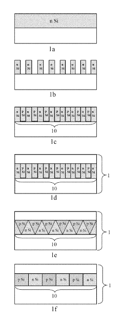
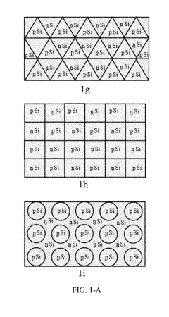
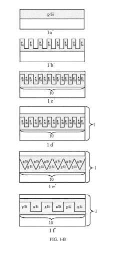
01 GaN HEMT structure for high-frequency applications
Gallium Nitride High Electron Mobility Transistors (HEMTs) are designed with specific structural features to enhance high-frequency performance. These transistors utilize a two-dimensional electron gas (2DEG) at the AlGaN/GaN interface, which provides high electron mobility and velocity. The structure typically includes optimized gate length, barrier layers, and channel designs to minimize parasitic capacitance and resistance, enabling operation at frequencies reaching into the millimeter-wave range.- High-frequency GaN transistor structures: Gallium Nitride (GaN) transistors can be designed with specific structural features to enhance high-frequency performance. These structures include optimized gate configurations, advanced channel designs, and specialized substrate materials that reduce parasitic capacitance and resistance. Such structural optimizations allow for improved electron mobility and reduced signal delay, enabling operation at higher frequencies with better efficiency and power handling capabilities.
- GaN growth techniques for high-frequency applications: Advanced growth techniques for Gallium Nitride materials significantly impact the performance of high-frequency transistors. Methods such as molecular beam epitaxy (MBE), metal-organic chemical vapor deposition (MOCVD), and hydride vapor phase epitaxy (HVPE) can be optimized to reduce defect density and improve crystal quality. These techniques enable the production of high-purity GaN layers with controlled doping profiles, which are essential for achieving superior high-frequency characteristics in transistors.
- Power amplification in GaN high-frequency transistors: Gallium Nitride transistors offer exceptional power amplification capabilities at high frequencies due to their wide bandgap properties and high electron mobility. These transistors can be designed with specific features to enhance power handling, thermal management, and linearity for RF and microwave applications. Advanced power amplifier configurations using GaN transistors enable higher output power, improved efficiency, and broader bandwidth operation compared to conventional semiconductor technologies.
- Thermal management in high-frequency GaN devices: Effective thermal management is crucial for high-frequency GaN transistors operating at elevated power levels. Various approaches include advanced heat sink designs, diamond heat spreaders, microfluidic cooling channels, and optimized device layouts to minimize thermal resistance. These thermal management techniques help maintain device reliability and performance by preventing excessive junction temperatures that could otherwise lead to performance degradation or premature device failure during high-frequency operation.
- Integration of GaN transistors in high-frequency circuits: Integration of Gallium Nitride transistors into high-frequency circuit designs requires specialized approaches to maximize performance. This includes optimized impedance matching networks, novel interconnect strategies, and co-integration with other semiconductor technologies. Advanced packaging techniques and circuit topologies specifically designed for GaN devices enable the full exploitation of their high-frequency capabilities while addressing challenges related to parasitic effects and signal integrity at microwave and millimeter-wave frequencies.
02 GaN transistor fabrication techniques for high-frequency performance
Advanced fabrication methods are crucial for producing high-frequency GaN transistors. These techniques include epitaxial growth processes like MOCVD or MBE to create high-quality GaN layers with minimal defects, specialized gate formation processes to achieve short gate lengths, and surface passivation to reduce trapping effects. Additionally, advanced metallization schemes and thermal management solutions are implemented to handle the high power densities while maintaining high-frequency performance.Expand Specific Solutions03 Power amplifier designs using GaN transistors
GaN transistors are integrated into power amplifier circuits specifically designed to leverage their high-frequency capabilities. These designs include matching networks optimized for GaN's unique characteristics, bias circuits that ensure stable operation under varying conditions, and thermal management solutions. The power amplifiers utilize GaN's high breakdown voltage and power density to achieve superior performance in terms of output power, efficiency, and linearity at high frequencies for applications in telecommunications, radar, and satellite communications.Expand Specific Solutions04 GaN-based RF switching and control circuits
GaN transistors are employed in high-frequency switching and control circuits that benefit from their fast switching speeds and high breakdown voltages. These circuits include RF switches, phase shifters, and modulators that operate at microwave and millimeter-wave frequencies. The designs incorporate specialized topologies to minimize insertion loss and maximize isolation, while addressing challenges related to linearity and power handling in high-frequency applications.Expand Specific Solutions05 Integration and packaging of GaN transistors for high-frequency systems
Advanced integration and packaging techniques are developed for GaN high-frequency transistors to maintain performance while enabling system-level functionality. These approaches include multi-chip modules, heterogeneous integration with other semiconductor technologies, and advanced thermal management solutions. The packaging designs minimize parasitic effects that would degrade high-frequency performance, incorporate efficient heat dissipation structures, and provide electromagnetic shielding to prevent interference in complex RF systems.Expand Specific Solutions
Key Industry Players in GaN Transistor Market
Gallium Nitride (GaN) transistors have emerged as a disruptive technology in high-frequency electronics, with the market currently in a growth phase characterized by increasing adoption across multiple sectors. The global GaN power device market is expanding rapidly, projected to reach $1.5-2 billion by 2025 with a CAGR of approximately 25%. Technology maturity varies across players, with established companies like Wolfspeed, GaN Systems, and Cambridge GaN Devices leading innovation in commercial applications, while Intel, Analog Devices, and MACOM are advancing integration capabilities. Newer entrants such as Dynax Semiconductor and Suzhou Jingzhan are focusing on specialized applications. Research institutions including CEA and KAUST are pushing fundamental boundaries, while defense contractors like Raytheon and Boeing are developing military-grade implementations, collectively driving GaN technology toward mainstream adoption in power electronics and RF applications.
MACOM Technology Solutions Holdings, Inc.
Technical Solution: MACOM has developed a comprehensive GaN-on-Silicon technology platform specifically optimized for RF and microwave applications. Their proprietary GaN-on-Si approach enables cost-effective manufacturing using standard 6-inch and 8-inch silicon wafer processing facilities. MACOM's GaN transistors operate at frequencies up to 40GHz with power densities of 4-5W/mm, delivering 70% power-added efficiency in S-band applications. Their scalable technology supports both discrete transistors and highly integrated multi-function MMICs (Monolithic Microwave Integrated Circuits). MACOM's GaN solutions feature advanced thermal management techniques including copper-filled through-wafer vias and diamond heat spreaders, enabling reliable operation at high power levels. Their devices demonstrate mean-time-to-failure exceeding 1 million hours at 200°C channel temperature with less than 10% performance degradation.
Strengths: Cost-effective GaN-on-Si manufacturing approach leveraging standard silicon infrastructure; extensive RF system expertise enabling optimized solutions; broad product portfolio spanning discrete devices to integrated MMICs. Weaknesses: Lower thermal conductivity compared to GaN-on-SiC alternatives; frequency limitations compared to competing technologies; challenges in very high-power applications.
GaN Systems, Inc.
Technical Solution: GaN Systems has pioneered island technology architecture for GaN power transistors, enabling higher current handling, superior thermal performance, and lower inductance. Their GaNPX packaging eliminates wire bonds and provides optimal thermal management, allowing frequencies up to 100MHz. The company's enhancement-mode GaN transistors operate at 650V and 100V ratings with switching speeds exceeding 100V/ns. Their patented design reduces parasitic inductance by over 90% compared to traditional packages, enabling power densities 4-5x higher than silicon solutions. GaN Systems' transistors demonstrate reliability with over 100 million device-hours of testing, showing stable performance even after 1000 hours of stress testing at 150°C.
Strengths: Industry-leading power density and switching speeds with minimal parasitic inductance; proprietary packaging technology enabling superior thermal performance; comprehensive reliability testing. Weaknesses: Higher initial cost compared to silicon alternatives; requires specialized gate drivers; thermal management remains challenging in extremely high-power applications.
Core Patents and Technical Literature on GaN Technology
Nitride power transistor and manufacturing method thereof
PatentActiveUS20190140088A1
Innovation
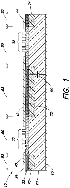
- A nitride power transistor is developed with a silicon substrate featuring a differently doped semiconductor composite structure forming a space charge depletion region, combined with a nitride epitaxial layer, which increases the breakdown voltage and includes a GaN capping layer and AlN insertion layer to enhance electron mobility and reduce surface defects.
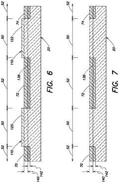
Parasitic capacitance reduction in GaN devices
PatentActiveUS11929364B2
Innovation
- Replacing a portion of the substrate between interconnects and the ground with a material having a lower dielectric constant, such as silicon dioxide, formed using a LOCOS process, to reduce parasitic capacitance.
Thermal Management Strategies for GaN Devices
Effective thermal management is critical for Gallium Nitride (GaN) devices due to their high power density and operating temperatures. As GaN transistors operate at significantly higher frequencies and power levels than silicon counterparts, they generate substantial heat that must be efficiently dissipated to maintain reliability and performance. The thermal conductivity of GaN (130-230 W/mK) is higher than silicon but lower than silicon carbide, necessitating specialized cooling strategies.
Active cooling techniques represent the first line of defense in GaN thermal management. Liquid cooling systems have proven particularly effective for high-power GaN applications, offering thermal resistance values as low as 0.1°C/W. Advanced microchannel coolers placed directly beneath GaN devices can remove heat fluxes exceeding 1000 W/cm², enabling operation at maximum power without thermal degradation.
Passive cooling approaches complement active systems through materials innovation. Diamond heat spreaders, with thermal conductivity up to 2000 W/mK, are increasingly integrated with GaN devices despite manufacturing challenges. Composite materials like copper-diamond and aluminum-silicon carbide provide balanced thermal performance at lower cost points, with thermal conductivities ranging from 400-700 W/mK.
Thermal interface materials (TIMs) play a crucial role in the thermal stack. Next-generation metal TIMs and graphene-enhanced compounds achieve thermal conductivities of 20-80 W/mK while maintaining necessary compliance for coefficient of thermal expansion matching. These materials reduce thermal boundary resistance at critical interfaces by up to 60% compared to conventional solutions.
Advanced packaging technologies further enhance thermal performance. Direct die-attach methods eliminate packaging layers that impede heat flow, reducing junction-to-case thermal resistance by 30-50%. Three-dimensional integrated cooling architectures embed microfluidic channels directly into device substrates, enabling junction temperature reductions of up to 40°C under maximum load conditions.
Computational fluid dynamics (CFD) modeling has become essential for optimizing GaN thermal solutions. Multiphysics simulation platforms now accurately predict temperature profiles within 5% of measured values, allowing designers to identify and address hotspots before physical prototyping. These tools enable evaluation of complex thermal interactions across multiple time scales, from microsecond transients to steady-state operation.
Industry standards for GaN thermal management continue to evolve, with JEDEC and IEEE developing specialized guidelines for wide-bandgap semiconductor cooling. These standards establish consistent measurement protocols and performance metrics, facilitating comparison between different thermal solutions and accelerating industry-wide adoption of best practices.
Cost-Performance Analysis of GaN vs Silicon Technologies
When evaluating the economic viability of Gallium Nitride (GaN) transistors compared to traditional silicon technologies, a comprehensive cost-performance analysis reveals several critical factors that influence adoption decisions in high-frequency electronics applications.
Initial manufacturing costs for GaN devices remain significantly higher than silicon counterparts, with production expenses typically 2-3 times greater due to more complex fabrication processes and lower manufacturing yields. The substrate materials for GaN transistors, particularly silicon carbide (SiC) or sapphire, contribute substantially to this cost differential, with high-quality substrates commanding premium prices in the supply chain.
However, the total cost of ownership calculation shifts favorably toward GaN when considering system-level economics. GaN-based systems often require fewer components due to higher power density capabilities, resulting in smaller form factors and reduced material costs for peripheral components. This integration advantage typically translates to 15-25% savings in overall bill of materials for complete electronic systems.
Energy efficiency represents another crucial economic factor. GaN transistors operate with significantly lower switching losses compared to silicon MOSFETs, with efficiency improvements of 5-10% commonly observed in power conversion applications. Over product lifetimes, these efficiency gains translate to substantial energy cost savings, particularly in data centers, telecommunications infrastructure, and other high-power applications where operating expenses dominate total ownership costs.
Reliability metrics further strengthen GaN's value proposition despite higher upfront costs. The superior thermal performance and breakdown characteristics of GaN devices extend operational lifetimes in demanding environments, reducing replacement frequency and associated maintenance costs. Mean time between failures (MTBF) data increasingly demonstrates favorable long-term economics for GaN solutions in mission-critical applications.
Market analysis indicates a steady decline in GaN manufacturing costs as production volumes increase and fabrication processes mature. Industry projections suggest price parity with silicon technologies in specific application segments within 3-5 years, driven by economies of scale and manufacturing innovations. This trend is accelerated by increasing competition among GaN device manufacturers and expanding application ecosystems.
The performance premium of GaN enables new capabilities that create value beyond direct component cost comparisons. In radar systems, wireless infrastructure, and satellite communications, the exceptional high-frequency performance of GaN enables functionality that silicon-based alternatives simply cannot match at any price point, creating entirely new market opportunities with distinct economic considerations.
Unlock deeper insights with Patsnap Eureka Quick Research — get a full tech report to explore trends and direct your research. Try now!
Generate Your Research Report Instantly with AI Agent
Supercharge your innovation with Patsnap Eureka AI Agent Platform!