Gallium Nitride Transistors vs Conventional Transistors: A Performance Review
OCT 14, 20259 MIN READ
Generate Your Research Report Instantly with AI Agent
Patsnap Eureka helps you evaluate technical feasibility & market potential.
GaN Transistor Evolution and Objectives
Gallium Nitride (GaN) transistors represent a significant evolution in semiconductor technology, emerging as a promising alternative to conventional silicon-based transistors. The development of GaN transistors began in the early 1990s, with initial research focusing on overcoming material growth challenges and understanding the unique properties of GaN as a wide-bandgap semiconductor. By the early 2000s, researchers had made substantial progress in developing viable GaN transistor prototypes, demonstrating their potential for high-frequency, high-power applications.
The technological trajectory of GaN transistors has been characterized by continuous improvements in material quality, device architecture, and manufacturing processes. Early GaN transistors suffered from reliability issues and high production costs, limiting their commercial viability. However, advancements in epitaxial growth techniques, particularly metal-organic chemical vapor deposition (MOCVD), have significantly enhanced the quality and consistency of GaN layers, enabling more reliable device performance.
A pivotal development in GaN transistor evolution was the introduction of High Electron Mobility Transistors (HEMTs) based on AlGaN/GaN heterostructures. These devices leverage the formation of a two-dimensional electron gas (2DEG) at the interface between AlGaN and GaN layers, resulting in exceptional electron mobility and current-carrying capability. This breakthrough has positioned GaN transistors as superior alternatives to silicon-based devices in applications requiring high power density and frequency response.
Recent trends in GaN transistor development include the integration with silicon substrates (GaN-on-Si), which has substantially reduced manufacturing costs while maintaining performance advantages. Additionally, researchers are exploring novel device architectures such as vertical GaN transistors and enhancement-mode GaN transistors to address specific application requirements and further improve performance metrics.
The primary objectives of current GaN transistor research and development efforts are multifaceted. First, there is a strong focus on enhancing reliability and operational lifetime to match or exceed those of conventional silicon devices. Second, researchers aim to reduce manufacturing costs through process optimization and economies of scale, making GaN technology more accessible across various market segments. Third, there is significant interest in expanding the application scope of GaN transistors beyond their traditional strongholds in RF and power electronics.
Looking forward, the evolution of GaN transistors is expected to continue along several trajectories: increasing power density capabilities, improving thermal management, enhancing integration with complementary technologies, and developing specialized variants for emerging applications such as electric vehicles, renewable energy systems, and next-generation communication infrastructure. The ultimate goal is to establish GaN transistors as a mainstream technology that can effectively address the limitations of conventional transistors in meeting the demands of future electronic systems.
Market Demand Analysis for GaN Power Devices
The global market for GaN power devices is experiencing robust growth, driven primarily by the increasing demand for high-efficiency power electronics across multiple sectors. Current market valuations place the GaN power device market at approximately 223 million USD in 2022, with projections indicating a compound annual growth rate (CAGR) of 33.4% through 2028, potentially reaching 1.24 billion USD by the end of the forecast period.
This accelerated market expansion is largely attributed to the superior performance characteristics of GaN transistors compared to conventional silicon-based alternatives. The automotive sector represents one of the most significant growth drivers, with electric vehicles (EVs) and hybrid electric vehicles (HEVs) requiring increasingly efficient power conversion systems. The adoption of GaN technology in onboard chargers and DC-DC converters has demonstrated efficiency improvements of 5-10% over silicon-based systems, translating to extended vehicle range and reduced charging times.
Consumer electronics constitutes another substantial market segment, with manufacturers increasingly incorporating GaN-based chargers and power adapters into their product ecosystems. The rapid charging capabilities and compact form factors enabled by GaN technology have resonated strongly with consumers, leading to premium pricing opportunities for manufacturers and accelerated adoption rates.
Industrial applications represent the third major market segment, with particular emphasis on renewable energy systems, industrial motor drives, and data center power supplies. The higher switching frequencies achievable with GaN transistors enable more compact and efficient power conversion systems, addressing critical pain points in these applications such as energy density, thermal management, and overall system efficiency.
Regional analysis reveals that Asia-Pacific currently dominates the GaN power device market, accounting for approximately 45% of global demand. This regional concentration is primarily due to the strong presence of semiconductor manufacturing infrastructure and consumer electronics production. North America and Europe follow with approximately 30% and 20% market share respectively, with particularly strong growth in automotive and industrial applications.
Market penetration analysis indicates that GaN technology has achieved approximately 3% penetration in the broader power semiconductor market, suggesting substantial room for growth as manufacturing scales and costs decrease. Industry forecasts suggest that by 2030, GaN devices could capture up to 15% of the power semiconductor market in specific application segments where their performance advantages are most pronounced.
Customer surveys indicate that the primary adoption barriers include cost premiums (currently 1.5-2x compared to silicon alternatives), reliability concerns in new applications, and the need for redesigned driver circuits and control systems to fully leverage GaN's performance capabilities.
GaN vs Silicon: Technical Challenges and Limitations
Despite the promising advantages of Gallium Nitride (GaN) transistors over conventional silicon-based transistors, several significant technical challenges and limitations hinder their widespread adoption. The fundamental material properties of GaN present unique fabrication difficulties. The lack of native GaN substrates forces manufacturers to grow GaN on foreign substrates like silicon carbide or sapphire, creating lattice mismatches that introduce defects and dislocations. These structural imperfections compromise device performance and reliability, particularly under high-stress operating conditions.
Thermal management represents another critical challenge. While GaN devices can operate at higher temperatures than silicon counterparts, they generate substantial heat during high-power operations. The thermal conductivity of GaN (130 W/mK) is superior to silicon (150 W/mK) but inferior to silicon carbide (490 W/mK), necessitating sophisticated thermal management solutions that add complexity and cost to overall system designs.
Gate leakage current remains problematic in GaN high-electron-mobility transistors (HEMTs). The Schottky barrier between the metal gate and semiconductor allows significant leakage current under high voltage conditions, degrading efficiency and reliability. Various gate insulation technologies are being explored, but each introduces additional manufacturing complexities and potential new failure modes.
Current collapse phenomenon, where dynamic on-resistance increases during switching operations, significantly impacts GaN transistor performance in power applications. This effect, attributed to electron trapping at surface states or in buffer layers, reduces efficiency and reliability in high-frequency switching applications. Passivation techniques and buffer layer optimization help mitigate this issue but add manufacturing complexity.
Manufacturing scalability presents substantial economic barriers. Silicon benefits from decades of manufacturing optimization and enormous economies of scale. GaN processing requires specialized equipment and techniques, resulting in higher production costs. The industry faces challenges in transitioning from small-diameter wafers to larger formats that would enable cost reduction through volume production.
Reliability concerns persist, particularly regarding device degradation mechanisms under high-field, high-temperature conditions. Time-dependent breakdown mechanisms in GaN devices differ from well-understood silicon failure modes, requiring new reliability models and accelerated life testing methodologies.
Integration challenges with conventional silicon-based circuitry create additional complications. The voltage levels, driving requirements, and protection circuits for GaN devices often differ from silicon counterparts, necessitating redesigned driver and control circuitry that increases system complexity and cost.
These technical limitations collectively explain why, despite GaN's superior theoretical performance metrics, silicon-based technologies continue to dominate many application spaces. Overcoming these challenges requires coordinated advances in materials science, device design, manufacturing processes, and system integration approaches.
Current GaN Implementation Approaches
01 High-frequency performance enhancement in GaN transistors
Gallium Nitride (GaN) transistors demonstrate superior high-frequency performance due to their wide bandgap properties. Various structural modifications and fabrication techniques can enhance their frequency response, making them suitable for RF and microwave applications. These enhancements include optimized gate designs, reduced parasitic capacitances, and improved electron mobility, resulting in higher cutoff frequencies and better power gain at high frequencies.- High-frequency performance enhancement techniques: Various techniques can be employed to enhance the high-frequency performance of Gallium Nitride (GaN) transistors. These include optimizing gate structures, reducing parasitic capacitances, and implementing advanced epitaxial layer designs. By carefully engineering these aspects, GaN transistors can achieve superior switching speeds and higher operating frequencies, making them suitable for RF and microwave applications. These enhancements enable improved power gain and efficiency at high frequencies compared to conventional semiconductor materials.
- Thermal management solutions for GaN transistors: Effective thermal management is crucial for maintaining the performance of GaN transistors under high-power operation. Various approaches include integrating heat dissipation structures, using advanced packaging techniques, and implementing thermal interface materials. These solutions help to reduce junction temperatures, prevent thermal runaway, and ensure reliable operation under demanding conditions. Improved thermal management directly contributes to enhanced device lifetime and sustained performance characteristics at elevated power levels.
- Material quality and defect reduction methods: The performance of GaN transistors is significantly influenced by the quality of the semiconductor material and the presence of defects. Advanced growth techniques, buffer layer optimization, and defect reduction strategies are employed to minimize dislocations and impurities in GaN epitaxial layers. By improving material quality, key performance parameters such as breakdown voltage, leakage current, and carrier mobility can be enhanced, leading to more efficient and reliable transistor operation.
- Novel device structures for performance improvement: Innovative device architectures are being developed to push the performance boundaries of GaN transistors. These include vertical device structures, field-plate designs, polarization engineering, and heterojunction configurations. Such novel structures help to overcome traditional limitations in power handling, breakdown voltage, and on-resistance. By optimizing the electric field distribution and charge transport mechanisms, these advanced designs enable GaN transistors to achieve superior figures of merit for power switching and amplification applications.
- Reliability enhancement and degradation mitigation: Ensuring long-term reliability is essential for GaN transistor performance in practical applications. Various approaches focus on mitigating degradation mechanisms such as current collapse, threshold voltage instability, and hot electron effects. These include surface passivation techniques, gate dielectric optimization, and field management structures. By addressing these reliability concerns, GaN transistors can maintain consistent performance characteristics over extended operating lifetimes under various stress conditions, making them suitable for demanding applications in power electronics and communications.
02 Thermal management and reliability improvements
GaN transistors exhibit excellent thermal conductivity and stability at high temperatures, which is crucial for high-power applications. Innovations in substrate materials, heat dissipation structures, and packaging techniques have significantly improved the thermal management of these devices. Enhanced thermal performance leads to better reliability, longer device lifetime, and sustained electrical performance under extreme operating conditions.Expand Specific Solutions03 Power handling capabilities and efficiency
GaN transistors offer superior power density and efficiency compared to conventional semiconductor materials. Their high breakdown voltage and electron saturation velocity enable them to handle higher power levels while maintaining efficiency. Advanced designs incorporating field plates, optimized buffer layers, and improved ohmic contacts have further enhanced their power handling capabilities, making them ideal for power amplification and high-voltage switching applications.Expand Specific Solutions04 Growth and fabrication techniques for improved performance
Various epitaxial growth methods and fabrication techniques have been developed to enhance GaN transistor performance. These include MOCVD, MBE, and advanced lithography processes that improve crystal quality and reduce defect density. Innovations in substrate selection, buffer layer design, and surface passivation have led to better electrical characteristics, reduced leakage currents, and enhanced overall device performance.Expand Specific Solutions05 Novel device structures and heterostructures
Innovative device architectures and heterostructures have been developed to push the performance boundaries of GaN transistors. These include AlGaN/GaN HEMTs, MIS-HEMTs, and vertical GaN transistors with novel gate configurations. The incorporation of other materials like InGaN and AlN in strategic device regions has enabled better carrier confinement, reduced short-channel effects, and improved switching characteristics, leading to enhanced overall performance metrics.Expand Specific Solutions
Key Manufacturers and Competitive Landscape
Gallium Nitride (GaN) transistors are emerging as a disruptive technology in the semiconductor industry, currently in the growth phase of market development. The global GaN power device market is expanding rapidly, projected to reach $1.75 billion by 2026 with a CAGR of approximately 35%. Technologically, GaN transistors offer superior performance over conventional silicon transistors with higher switching speeds, better thermal conductivity, and smaller form factors. Leading players like Wolfspeed, Navitas Semiconductor, and GaN Systems are driving innovation, while established semiconductor giants including Texas Instruments, Intel, NXP, and Panasonic are increasing investments in GaN technology. Research institutions such as Xidian University and Cambridge Enterprise are advancing fundamental research, while companies like MACOM and Raytheon focus on defense and RF applications. The technology is approaching mainstream adoption in power electronics, telecommunications, and automotive sectors.
Texas Instruments Incorporated
Technical Solution: Texas Instruments has developed an extensive portfolio of GaN transistors and supporting components targeting high-efficiency power conversion applications. Their GaN technology utilizes a GaN-on-Si approach to balance performance and cost-effectiveness. TI's latest generation devices feature enhancement-mode operation with threshold voltages compatible with conventional gate drivers, simplifying implementation. Their GaN FETs achieve RDS(on) values as low as 2mΩ with breakdown voltages up to 700V[7]. TI has implemented advanced field plate structures in their GaN transistors to manage peak electric fields and enhance reliability. Their devices demonstrate switching speeds exceeding 200V/ns with minimal dynamic RDS(on) effects that plague many competing solutions. TI's manufacturing approach leverages their existing silicon infrastructure, enabling high-volume production with excellent process control. Their GaN portfolio includes both discrete transistors and integrated solutions that combine GaN power stages with optimized drivers and protection features. TI has developed comprehensive design tools and reference designs that help customers transition from silicon to GaN technology while maximizing performance benefits[8].
Strengths: Extensive ecosystem of supporting components and design resources, enhancement-mode operation simplifies implementation, and manufacturing approach enables competitive pricing. Weaknesses: Performance metrics slightly behind some GaN-only specialists, thermal management can be challenging in high-power applications, and requires careful attention to layout to minimize parasitic inductances.
NXP USA, Inc.
Technical Solution: NXP has developed a comprehensive GaN transistor portfolio targeting automotive, industrial, and communications applications. Their RF GaN technology utilizes a proprietary GaN-on-SiC process that achieves power-added efficiencies exceeding 70% at frequencies up to 3.5 GHz[5]. For power applications, NXP offers GaN-on-Si devices with breakdown voltages up to 650V and RDS(on) values as low as 25mΩ. Their transistors feature advanced thermal management designs with junction-to-case thermal resistances below 0.5°C/W, enabling sustained high-power operation. NXP's GaN devices incorporate sophisticated gate structures that minimize threshold voltage shifts over temperature and time, addressing a key reliability concern with GaN technology. Their manufacturing process employs advanced epitaxial growth techniques that reduce defect densities to below 10⁹ cm⁻², significantly enhancing long-term reliability[6]. NXP has also developed specialized driver ICs optimized for their GaN transistors, creating complete solution sets that simplify customer implementation and maximize performance benefits compared to conventional silicon transistors.
Strengths: Comprehensive product portfolio spanning multiple applications, excellent thermal performance enabling sustained high-power operation, and specialized driver ICs that optimize system-level performance. Weaknesses: Higher cost structure compared to silicon alternatives, requires careful PCB layout to minimize parasitic effects, and faces competition from both established semiconductor companies and GaN specialists.
Critical Patents and Breakthroughs in GaN Technology
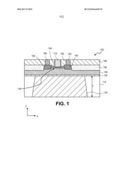
Gallium nitride transistor with underfill aluminum nitride for improved thermal and RF performance
PatentWO2017171870A1
Innovation
- Incorporating an aluminum nitride layer under the gallium nitride transistor or circuit block, utilizing a low resistivity silicon substrate, which provides both high thermal conductivity and high resistivity through the aluminum nitride's insulating properties and superior thermal conductivity compared to silicon.
Bidirectional transistor having a low resistance heterojunction in an on state
PatentActiveUS20200098908A1
Innovation
- A bidirectional heterojunction field-effect transistor design with a silicon substrate, featuring a GaN layer and an AlGaN barrier layer, where the control gates extend transversely and are biased relative to reference electrodes, reducing the on-state resistance and footprint by optimizing the distance between conduction electrodes and control gates.
Thermal Management Solutions for GaN Devices
Thermal management represents a critical challenge in the widespread adoption of Gallium Nitride (GaN) transistor technology. While GaN devices offer superior performance characteristics compared to conventional silicon-based transistors, they generate significant heat during operation due to their high power density capabilities. This thermal challenge necessitates innovative cooling solutions to maintain optimal performance and reliability.
Traditional cooling methods such as passive heat sinks and forced-air cooling have proven inadequate for high-power GaN applications. The thermal conductivity of GaN (130 W/mK) is higher than silicon (150 W/mK), but the concentrated heat generation in smaller device footprints creates localized hotspots that conventional cooling struggles to address effectively.
Advanced thermal interface materials (TIMs) have emerged as a promising solution for GaN devices. Diamond-based TIMs with thermal conductivity exceeding 1500 W/mK offer superior heat dissipation compared to conventional thermal greases (1-5 W/mK). These materials create more efficient thermal pathways from the GaN device to the heat sink, reducing junction temperatures by up to 30%.
Liquid cooling systems have demonstrated exceptional effectiveness for high-power GaN applications. Direct liquid cooling, where a dielectric fluid directly contacts the GaN device, has shown the ability to handle heat fluxes exceeding 1000 W/cm², representing a 5-10x improvement over air cooling. Two-phase cooling systems utilizing the latent heat of vaporization can achieve even higher cooling efficiencies.
Microfluidic cooling channels integrated directly into GaN device packaging represent another innovative approach. These microscale channels allow coolant to flow in close proximity to the heat source, reducing thermal resistance by up to 60% compared to conventional cooling methods. Recent research has demonstrated successful integration of these channels without compromising electrical performance.
Advanced substrate materials also play a crucial role in GaN thermal management. Silicon carbide (SiC) substrates offer 3x better thermal conductivity than silicon, while diamond substrates can provide up to 10x improvement. Though diamond substrates remain prohibitively expensive for most commercial applications, composite substrates incorporating diamond particles have emerged as cost-effective alternatives.
Active cooling technologies such as thermoelectric coolers and piezoelectric micro-fans are being explored for specialized GaN applications. These solutions offer precise temperature control capabilities but face efficiency and integration challenges that limit their widespread adoption in current commercial products.
Cost-Performance Analysis of GaN Adoption
The adoption of Gallium Nitride (GaN) transistors represents a significant investment decision for manufacturers and system designers. When evaluating the cost-performance trade-offs, several key factors must be considered beyond the initial higher unit price of GaN devices compared to conventional silicon-based transistors.
Manufacturing costs for GaN transistors currently remain 2-3 times higher than silicon counterparts due to more complex fabrication processes and lower production volumes. However, this cost differential has been steadily decreasing at approximately 15% annually as manufacturing techniques mature and economies of scale improve. Industry projections suggest potential cost parity in specific application segments within 5-7 years.
Performance advantages translate into significant system-level cost benefits that often outweigh the higher component costs. GaN's superior switching speeds enable the use of smaller passive components (inductors, capacitors), reducing overall bill of materials costs by 20-30% in many power conversion applications. The higher efficiency (typically 2-5% improvement) directly reduces cooling requirements, allowing for smaller heatsinks and simplified thermal management systems.
Reliability metrics indicate GaN transistors maintain performance advantages over longer operational lifetimes in high-temperature and high-frequency applications. Mean Time Between Failures (MTBF) data shows comparable or better reliability than silicon devices in controlled environments, potentially reducing maintenance and replacement costs over system lifetime.
Total Cost of Ownership (TCO) analysis reveals that GaN-based systems typically achieve break-even within 1-3 years for high-utilization applications like data centers, telecommunications, and industrial power supplies. The energy savings alone can offset the initial premium, with documented cases showing 3-7% reduction in operational expenses for power-intensive applications.
Market segmentation analysis indicates that GaN adoption is economically justified today in premium applications where performance and size constraints are primary considerations. Mass-market adoption faces continued cost barriers, though the expanding middle segment represents the current battleground where GaN is increasingly competitive on a TCO basis. Automotive and consumer electronics represent the next major adoption frontiers as costs continue to decline.
Unlock deeper insights with Patsnap Eureka Quick Research — get a full tech report to explore trends and direct your research. Try now!
Generate Your Research Report Instantly with AI Agent
Supercharge your innovation with Patsnap Eureka AI Agent Platform!