The Role of Intellectual Property on Gallium Nitride Transistor Advancements
OCT 14, 202510 MIN READ
Generate Your Research Report Instantly with AI Agent
Patsnap Eureka helps you evaluate technical feasibility & market potential.
GaN Transistor IP Evolution and Objectives
Gallium Nitride (GaN) transistor technology has evolved significantly since its inception in the early 1990s, transforming from a laboratory curiosity to a commercial reality with profound implications for power electronics, RF communications, and high-frequency applications. The intellectual property landscape surrounding GaN transistors has played a pivotal role in shaping this evolution, creating both opportunities and barriers for technological advancement.
The development of GaN transistor technology can be traced back to the pioneering work at universities and research institutions, where fundamental patents on material growth, device structures, and fabrication processes were first established. These early patents laid the groundwork for subsequent commercial development, with companies like Cree (now Wolfspeed), Nitronex (later acquired by MACOM), and International Rectifier (now part of Infineon) securing strategic IP positions.
Throughout the 2000s, the GaN IP landscape became increasingly complex as more players entered the field. Major semiconductor companies began acquiring startups with promising GaN technology portfolios, consolidating IP ownership and creating powerful patent estates. This period saw the emergence of distinct IP clusters around specific applications such as power switching, RF amplification, and high-voltage operation.
The objectives of IP strategy in the GaN transistor space have evolved from simply protecting core innovations to enabling broader ecosystem development. Early IP strategies focused on establishing fundamental claims over material compositions and basic device structures. As the technology matured, IP objectives shifted toward application-specific implementations, manufacturing techniques, and reliability enhancements.
Current IP trends in GaN transistors reflect the technology's commercial maturation. Patent filings increasingly focus on system-level integration, packaging innovations, and specialized circuit topologies that leverage GaN's unique properties. Additionally, there is growing emphasis on IP related to cost reduction techniques and manufacturing scalability, as these factors are critical for broader market adoption.
Looking forward, the IP landscape for GaN transistors is expected to evolve toward more collaborative models. Cross-licensing agreements and patent pools are becoming more common as industry participants recognize that fragmented IP ownership can impede overall market growth. Strategic objectives now include not only protecting proprietary technology but also ensuring freedom to operate in an increasingly crowded IP space.
The geographical distribution of GaN transistor IP has also shifted significantly. While early patents were predominantly filed in the United States, Japan, and Europe, recent years have seen substantial growth in Chinese patent activity, reflecting the country's strategic investment in semiconductor technology independence. This changing global IP landscape has important implications for market access and technology transfer strategies.
Market Analysis for GaN Power Electronics
The GaN power electronics market has experienced remarkable growth in recent years, driven by the superior performance characteristics of gallium nitride technology compared to traditional silicon-based solutions. The global market for GaN power devices was valued at approximately $1.4 billion in 2022 and is projected to reach $6.5 billion by 2028, representing a compound annual growth rate (CAGR) of over 29%. This exponential growth trajectory underscores the increasing adoption of GaN technology across various industries.
Consumer electronics represents the largest application segment, accounting for roughly 35% of the market share. The demand for faster charging solutions for smartphones, tablets, and laptops has been a significant driver, with GaN-based chargers offering smaller form factors and higher efficiency. Major consumer electronics manufacturers have begun incorporating GaN technology into their product ecosystems, further accelerating market penetration.
The automotive sector presents the fastest-growing opportunity for GaN power electronics, particularly in electric vehicle (EV) applications. GaN-based power systems can significantly improve the efficiency of onboard chargers, DC-DC converters, and inverters, thereby extending vehicle range and reducing charging times. Industry analysts predict that by 2026, approximately 22% of new EVs will incorporate some form of GaN power electronics.
Industrial applications constitute another substantial market segment, with GaN technology being increasingly deployed in motor drives, industrial power supplies, and renewable energy systems. The superior switching performance of GaN transistors enables higher frequency operation, resulting in smaller passive components and overall system size reduction.
Regional analysis reveals that Asia-Pacific dominates the GaN power electronics market, accounting for approximately 45% of global revenue. This dominance is attributed to the strong presence of semiconductor manufacturing facilities and consumer electronics production in countries like China, Japan, and South Korea. North America follows with roughly 30% market share, driven by significant investments in defense applications and electric vehicle infrastructure.
The market landscape is characterized by both established semiconductor giants and specialized GaN technology startups. Intellectual property considerations have significantly shaped market dynamics, with patent portfolios serving as critical competitive advantages. Companies with strong IP positions in GaN transistor technology have secured favorable market positions through licensing agreements and strategic partnerships.
Despite the promising growth outlook, market challenges persist, including relatively higher production costs compared to silicon alternatives and reliability concerns in certain high-stress applications. However, ongoing technological advancements and economies of scale are gradually addressing these limitations, paving the way for broader GaN adoption across diverse market segments.
Global IP Landscape and Technical Barriers
The global intellectual property landscape for Gallium Nitride (GaN) transistors reveals a complex network of patents and technical barriers that significantly influence technological advancement in this field. Patent filings for GaN transistor technology have experienced exponential growth over the past decade, with major concentrations in the United States, Japan, China, South Korea, and Germany. These regions collectively account for approximately 85% of all GaN-related patents, indicating the strategic importance of this technology in advanced semiconductor markets.
The United States maintains leadership in fundamental GaN transistor architecture patents, particularly through corporations like Cree/Wolfspeed, Texas Instruments, and research institutions such as MIT and Stanford University. Japan dominates in manufacturing process patents, with companies like Fujitsu, Panasonic, and Toshiba holding substantial IP portfolios focused on production efficiency and quality control methodologies.
China has rapidly emerged as a significant player, with patent filings increasing at an annual rate of approximately 30% since 2015. Chinese entities primarily focus on application-specific implementations and cost-effective manufacturing techniques, though they lag in fundamental technology patents. European entities, particularly in Germany and France, have specialized in GaN applications for automotive and industrial power systems.
Several critical technical barriers are evident in the global IP landscape. First, thermal management remains a significant challenge, with numerous patents addressing heat dissipation techniques but no definitive solution achieving industry-wide adoption. Companies like Infineon and ON Semiconductor hold strategic patents in this area, creating potential bottlenecks for competitors.
Second, reliability and degradation mechanisms continue to present obstacles, with patent clusters forming around passivation techniques and buffer layer designs. These patents often create complex licensing requirements that smaller entities struggle to navigate.
Third, integration with silicon-based technologies represents another barrier, with key patents controlled by a small number of entities including Intel and Samsung. This concentration creates potential chokepoints in the development of hybrid semiconductor solutions.
The patent landscape also reveals significant standardization challenges. Unlike more mature semiconductor technologies, GaN transistors lack comprehensive industry standards, resulting in fragmented IP portfolios that complicate cross-licensing agreements. This fragmentation has led to several high-profile litigation cases, particularly regarding epitaxial growth techniques and device structure patents.
Geopolitical factors further complicate the IP landscape, with increasing restrictions on technology transfer between certain regions creating artificial barriers to collaborative development. These restrictions particularly impact international research partnerships and technology licensing agreements in the GaN transistor space.
Current IP-Protected GaN Transistor Solutions
01 GaN Transistor Fabrication Methods
Various methods for fabricating gallium nitride transistors, including epitaxial growth techniques, substrate preparation, and layer deposition processes. These methods focus on improving the quality of GaN layers and optimizing the transistor structure for enhanced performance. Techniques include molecular beam epitaxy (MBE), metal-organic chemical vapor deposition (MOCVD), and hydride vapor phase epitaxy (HVPE) to create high-quality GaN layers with minimal defects.- GaN transistor fabrication methods: Various methods for fabricating gallium nitride transistors, including epitaxial growth techniques, substrate preparation, and device structure formation. These methods focus on improving the quality of GaN layers, reducing defects, and enhancing device performance through optimized growth conditions and processing steps.
- High electron mobility transistor (HEMT) structures: Design and implementation of GaN-based high electron mobility transistors, which utilize the two-dimensional electron gas formed at the interface between GaN and AlGaN layers. These structures offer high power density, high frequency operation, and improved thermal performance for power electronics and RF applications.
- Power electronics applications: Implementation of gallium nitride transistors in power electronic circuits and systems, leveraging their high breakdown voltage, low on-resistance, and fast switching capabilities. These applications include power converters, motor drives, and high-efficiency power supplies that benefit from GaN's superior performance compared to silicon-based devices.
- GaN substrate and material quality improvements: Techniques for improving the quality of gallium nitride materials and substrates used in transistor fabrication, including defect reduction methods, novel growth approaches, and substrate engineering. These improvements address challenges such as lattice mismatch, thermal expansion differences, and crystal defects that affect device performance and reliability.
- Novel device architectures and enhancements: Innovative gallium nitride transistor architectures and structural enhancements designed to improve performance metrics such as breakdown voltage, current density, and thermal management. These include vertical device structures, field plate designs, novel gate configurations, and integration techniques that push the boundaries of GaN transistor capabilities.
02 High Electron Mobility Transistor (HEMT) Structures
Design and implementation of GaN-based High Electron Mobility Transistor structures that leverage the two-dimensional electron gas (2DEG) formed at the AlGaN/GaN interface. These transistors feature high electron mobility, high breakdown voltage, and excellent high-frequency performance. The structures typically include buffer layers, channel layers, barrier layers, and specialized contact formations to optimize electron transport and minimize parasitic effects.Expand Specific Solutions03 GaN Substrate Development and Defect Reduction
Techniques for developing high-quality gallium nitride substrates and reducing defect densities in GaN layers. These approaches include specialized growth methods, buffer layer designs, and post-growth treatments to minimize dislocations, cracks, and other crystallographic defects that can degrade transistor performance. Methods such as epitaxial lateral overgrowth (ELO) and patterned substrates are employed to achieve lower defect densities.Expand Specific Solutions04 Power Electronics Applications of GaN Transistors
Implementation of gallium nitride transistors in power electronic applications, leveraging their high breakdown voltage, high switching speed, and low on-resistance. These transistors enable more efficient power conversion systems with higher power density compared to silicon-based devices. Applications include power supplies, motor drives, inverters, and other high-power switching circuits where GaN's superior properties provide significant performance advantages.Expand Specific Solutions05 GaN Transistor Reliability and Performance Enhancement
Methods to enhance the reliability and performance of gallium nitride transistors, including surface passivation techniques, gate engineering, thermal management solutions, and specialized contact formations. These approaches address common failure mechanisms such as current collapse, gate leakage, and thermal degradation. Advanced device architectures and novel materials are employed to extend device lifetime and improve operational stability under harsh conditions.Expand Specific Solutions
Key Patent Holders and Industry Competitors
The gallium nitride (GaN) transistor market is currently in a growth phase, with increasing adoption across power electronics, RF applications, and telecommunications. The global market size is expanding rapidly, projected to reach several billion dollars by 2026, driven by demand for high-efficiency power conversion and 5G infrastructure. Technologically, GaN transistors are approaching maturity in certain applications while still evolving in others. Key players shaping the intellectual property landscape include established semiconductor giants like Intel, Samsung Electronics, and Taiwan Semiconductor Manufacturing Co., alongside specialized GaN innovators such as Efficient Power Conversion Corp. and Transphorm Technology. Companies like MACOM, NXP, and Infineon are actively building strategic patent portfolios, while research institutions including Xidian University and North Carolina State University contribute fundamental innovations. This competitive environment has created complex IP dynamics where cross-licensing and strategic acquisitions increasingly determine market access and commercialization capabilities.
NXP USA, Inc.
Technical Solution: NXP has developed a significant GaN IP portfolio focused on RF applications, particularly for cellular infrastructure, defense, and aerospace markets. Their intellectual property covers specialized GaN-on-SiC (Silicon Carbide) technology optimized for high-power RF performance, with patents addressing epitaxial layer structures, device geometries, and thermal management techniques. NXP's GaN technology enables power densities exceeding 4W/mm at frequencies up to 40GHz, representing a 5-10x improvement over conventional technologies. Their IP portfolio includes advanced passivation techniques to enhance reliability under high-voltage operation and specialized approaches to mitigate electron trapping effects that can degrade RF performance. NXP has developed proprietary process control monitoring and reliability testing methodologies specifically tailored to GaN technology requirements. Their manufacturing approach leverages internal compound semiconductor fabrication capabilities combined with strategic foundry partnerships to ensure scalable production. NXP has systematically expanded their GaN product portfolio to address emerging applications including 5G massive MIMO systems, radar systems, and high-efficiency power amplifiers for both commercial and defense applications.
Strengths: Extensive RF system expertise enables optimized GaN solutions; established relationships with defense and aerospace customers; vertical integration of design and manufacturing; comprehensive modeling and characterization capabilities. Weaknesses: Primary focus on RF rather than power conversion applications; higher cost structure of GaN-on-SiC compared to GaN-on-Silicon alternatives; faces competition from specialized RF GaN providers.
INFINEON TECHNOLOGIES AMERICAS CORP
Technical Solution: Infineon has built a substantial GaN IP portfolio through both internal development and strategic acquisitions, including their purchase of International Rectifier which brought significant GaN expertise. Their CoolGaN™ technology platform represents a major focus of their intellectual property strategy, with patents covering both enhancement-mode and cascode device architectures. Infineon's IP extends beyond basic device structures to include specialized gate driver integration, thermal management techniques, and advanced packaging solutions optimized for GaN's unique characteristics. Their patent portfolio includes innovative approaches to managing dynamic RDS(on) effects and addressing current collapse phenomena that can impact GaN reliability. Infineon has developed proprietary screening and qualification methodologies for GaN devices that exceed standard silicon qualification requirements, addressing the unique failure mechanisms in GaN technology. Their manufacturing approach leverages existing silicon infrastructure while incorporating specialized process steps for GaN epitaxial growth and device fabrication. Infineon has systematically expanded their GaN product portfolio from initial 600V offerings to include 400V and 100V options, supported by comprehensive application-specific reference designs that help customers implement GaN solutions effectively.
Strengths: Extensive manufacturing infrastructure and quality systems; comprehensive product portfolio spanning multiple voltage classes; strong system-level expertise including gate drivers and controllers; global technical support capabilities. Weaknesses: Later market entry compared to some GaN specialists; balancing investment across silicon carbide and GaN technologies may dilute focus; higher cost structure of vertically integrated manufacturer.
Critical Patents and Technical Innovations
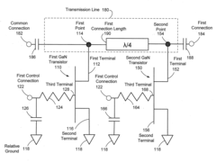
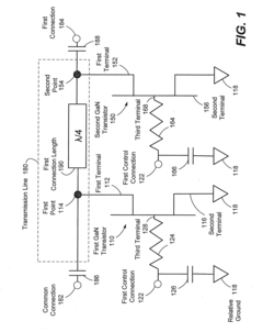
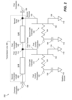
Gallium nitride switch methodology
PatentActiveUS20100097119A1
Innovation
- Configuring GaN-based transistors in a shunt configuration with transmission lines, where each transistor has a terminal coupled to the transmission line and another to ground, allowing signal control through the gate, and incorporating quarter-wavelength connection lengths to improve isolation by presenting an open circuit to the remaining device.
Gallium nitride material devices and associated methods
PatentActiveUS20070272957A1
Innovation
- Incorporating a source field plate made of conductive material connected to the source electrode, which reduces electrical fields between the gate and drain electrodes, thereby reducing gate-drain feedback capacitance, surface electron concentration, and increasing breakdown voltage, enabling transistors to operate at high drain efficiencies and output powers.
Licensing Models and Cross-Industry Collaboration
The intellectual property landscape surrounding Gallium Nitride (GaN) transistor technology has evolved significantly, giving rise to diverse licensing models that facilitate technological advancement while protecting innovation. Traditional exclusive licensing approaches have gradually shifted toward more collaborative frameworks, recognizing that GaN technology development requires substantial cross-disciplinary expertise and investment.
Patent pools have emerged as a prominent licensing model in the GaN transistor ecosystem, allowing multiple patent holders to license their technologies collectively. This approach has proven particularly effective for standardizing GaN technology implementations across industries while reducing transaction costs and mitigating litigation risks. Notable examples include the formation of GaN semiconductor consortia where companies like Infineon, Texas Instruments, and Cree/Wolfspeed participate in structured IP sharing arrangements.
Cross-industry collaboration has become increasingly vital as GaN transistors find applications beyond their original power electronics domain. Telecommunications companies partnering with automotive manufacturers, for instance, have established joint development agreements (JDAs) that include specific IP provisions for technology sharing while maintaining competitive advantages. These agreements typically include field-of-use restrictions that allow partners to leverage GaN technology in their respective industries without direct competition.
Open innovation platforms represent another emerging model, where certain foundational GaN transistor technologies are made available through open-source licensing while advanced implementations remain proprietary. This hybrid approach has accelerated adoption in emerging markets while allowing technology leaders to maintain competitive differentiation through proprietary enhancements. The "GaN Commons" initiative exemplifies this trend, providing basic design libraries while encouraging participants to contribute improvements under agreed licensing terms.
University-industry partnerships have created specialized licensing frameworks for GaN technology transfer. Academic institutions developing fundamental GaN transistor innovations often employ tiered licensing structures that offer preferential terms to industry partners who contribute to research funding. These arrangements typically include provisions for publication rights balanced against commercial exclusivity periods, fostering both academic advancement and industrial application.
Regional variations in IP strategies have also shaped collaboration models, with Asian manufacturers often forming technology alliances that pool patents regionally before engaging in global licensing negotiations. European consortia have emphasized standardization-focused licensing that prioritizes interoperability, while North American entities typically favor venture-based licensing structures that support startup commercialization of university-developed GaN technologies.
Regulatory Framework for GaN Semiconductor IP
The regulatory landscape governing Gallium Nitride (GaN) semiconductor intellectual property has evolved significantly over the past decade, creating a complex framework that both protects innovation and potentially limits market access. International patent systems, including those administered by the World Intellectual Property Organization (WIPO), the United States Patent and Trademark Office (USPTO), and the European Patent Office (EPO), have established specific classification categories for GaN-based technologies, reflecting their growing importance in the semiconductor industry.
Key regulatory considerations for GaN semiconductor IP include patent eligibility criteria, which vary across jurisdictions. In the United States, following decisions like Alice Corp. v. CLS Bank International, there has been increased scrutiny of patent claims related to semiconductor applications to ensure they represent more than abstract ideas. The European approach emphasizes technical contribution and inventive step, while Asian markets like Japan and China have developed specialized examination guidelines for semiconductor technologies.
Export control regulations present another critical dimension of the GaN IP regulatory framework. Due to the dual-use nature of GaN technology—applicable in both civilian and military contexts—many countries have implemented restrictions on technology transfer. The Wassenaar Arrangement, which includes 42 participating states, specifically addresses semiconductor manufacturing equipment and materials, including those related to GaN development. The U.S. Export Administration Regulations (EAR) and International Traffic in Arms Regulations (ITAR) impose particularly stringent controls on GaN technology transfer.
Standard-setting organizations (SSOs) have emerged as influential regulatory bodies in the GaN ecosystem. Organizations such as the IEEE, JEDEC, and IEC have developed technical standards that impact GaN transistor design and implementation. These standards often incorporate patented technologies, necessitating fair, reasonable, and non-discriminatory (FRAND) licensing commitments from patent holders. The interplay between standards and patents creates a quasi-regulatory environment that shapes market access and technology adoption.
Antitrust and competition law also significantly impact the GaN IP landscape. Patent pools and cross-licensing agreements, common in the semiconductor industry, must navigate complex antitrust regulations to avoid allegations of anti-competitive behavior. Recent enforcement actions by the European Commission, U.S. Federal Trade Commission, and China's State Administration for Market Regulation have specifically addressed licensing practices in the semiconductor sector, establishing precedents that affect GaN technology commercialization.
The regulatory framework continues to evolve in response to emerging challenges, including the protection of trade secrets related to GaN manufacturing processes and the treatment of AI-generated inventions in semiconductor design. As GaN transistor technology advances toward mainstream adoption, navigating this complex regulatory landscape has become a critical strategic consideration for industry participants seeking to protect their innovations while ensuring market access.
Unlock deeper insights with Patsnap Eureka Quick Research — get a full tech report to explore trends and direct your research. Try now!
Generate Your Research Report Instantly with AI Agent
Supercharge your innovation with Patsnap Eureka AI Agent Platform!