Investigating Coating Materials for Gallium Nitride Transistor Longevity
OCT 14, 20259 MIN READ
Generate Your Research Report Instantly with AI Agent
Patsnap Eureka helps you evaluate technical feasibility & market potential.
GaN Transistor Coating Background and Objectives
Gallium Nitride (GaN) transistors have emerged as a revolutionary technology in power electronics over the past two decades, offering superior performance characteristics compared to traditional silicon-based devices. The evolution of GaN technology began in the early 1990s with fundamental research into wide bandgap semiconductors, but significant commercial applications only materialized in the 2000s. This technology has progressively advanced from laboratory curiosity to mainstream adoption in high-frequency, high-power applications.
The inherent properties of GaN, including higher electron mobility, larger bandgap, and higher breakdown voltage, enable these transistors to operate at higher frequencies, temperatures, and power densities than silicon alternatives. However, these performance advantages come with unique challenges, particularly regarding long-term reliability and operational stability under extreme conditions.
A critical factor limiting GaN transistor longevity is surface degradation and interface instability. Environmental factors such as moisture, oxygen, and thermal cycling can significantly impact device performance over time. This degradation manifests as threshold voltage shifts, increased leakage currents, and ultimately, device failure. The industry has recognized that appropriate protective coating materials are essential to mitigate these effects and extend device lifetime.
The technical evolution trajectory shows a clear progression from basic passivation techniques to advanced multi-layer coating systems. Early approaches focused on simple silicon nitride or silicon dioxide passivation layers, while current research explores nanocomposite materials, atomic layer deposition techniques, and novel organic-inorganic hybrid coatings with enhanced barrier properties.
The primary objective of this investigation is to comprehensively evaluate existing and emerging coating materials for GaN transistors, with specific focus on enhancing operational longevity in harsh environments. We aim to identify coating solutions that can effectively protect against moisture ingress, prevent oxidation, maintain thermal stability, and preserve electrical characteristics over extended operational periods.
Secondary objectives include quantifying the impact of various coating materials on thermal management, as heat dissipation remains a critical factor in high-power applications. Additionally, we seek to establish correlations between coating composition, deposition methods, and long-term reliability metrics to develop predictive models for device lifetime.
The investigation also aims to explore cost-effective manufacturing approaches that can be scaled for high-volume production without compromising performance. This includes evaluation of novel deposition techniques and assessment of their compatibility with existing semiconductor manufacturing processes.
By addressing these objectives, this research seeks to contribute to the broader goal of establishing GaN technology as a reliable alternative to silicon in demanding applications such as electric vehicles, renewable energy systems, and next-generation telecommunications infrastructure.
Market Analysis for GaN Transistor Protective Coatings
The global market for GaN transistor protective coatings is experiencing robust growth, driven primarily by the expanding applications of GaN technology across multiple industries. Current market valuations indicate that the GaN semiconductor market reached approximately 1.4 billion USD in 2022, with protective coatings representing a significant segment within this ecosystem. Industry analysts project a compound annual growth rate (CAGR) of 18-20% for GaN-related protective materials through 2028, outpacing many other semiconductor segments.
The demand for specialized coating materials stems from several market forces. Power electronics represents the largest application segment, accounting for roughly 45% of the total market share. This is followed by telecommunications infrastructure at 25%, automotive applications at 15%, and aerospace and defense at 10%. The remaining market share is distributed among consumer electronics and emerging applications.
Regionally, Asia-Pacific dominates the market landscape, contributing approximately 60% of global demand, with particular concentration in Japan, South Korea, Taiwan, and increasingly China. North America follows at 25%, with Europe accounting for 12% of the market. The remaining 3% is distributed across other regions, with notable growth potential in emerging economies.
Key market drivers include the increasing adoption of electric vehicles, where GaN transistors offer significant efficiency improvements in power conversion systems. The 5G infrastructure rollout represents another substantial demand catalyst, with GaN-based systems providing superior performance in high-frequency applications. Additionally, the renewable energy sector's growth has created new opportunities for GaN technology in power inverters and energy storage systems.
Customer segments demonstrate varying priorities regarding coating materials. Defense and aerospace customers prioritize reliability and longevity over cost considerations, while consumer electronics manufacturers emphasize cost-effectiveness and scalability. Automotive tier-one suppliers occupy a middle ground, requiring both reliability and reasonable cost structures.
Market challenges include supply chain vulnerabilities, particularly for rare earth elements used in some coating formulations. Price sensitivity remains high in consumer-oriented applications, creating barriers to adoption for premium coating solutions. Additionally, the market faces competitive pressure from alternative technologies such as silicon carbide (SiC) transistors, which compete directly with GaN in certain applications.
Emerging market opportunities include the development of specialized coatings for extreme environment applications, such as space technology and deep-sea equipment. The miniaturization trend in electronics also creates demand for thinner yet more effective protective layers, opening new market segments for advanced coating technologies.
Current Challenges in GaN Transistor Protection
Despite significant advancements in gallium nitride (GaN) transistor technology, several critical challenges persist in developing effective protection mechanisms for these high-performance semiconductor devices. The primary issue facing GaN transistors is their vulnerability to environmental factors, particularly moisture and oxygen penetration, which can significantly degrade device performance and reduce operational lifespan. When exposed to these elements, GaN transistors experience accelerated oxidation at the surface, leading to increased leakage currents, threshold voltage shifts, and ultimately premature device failure.
Thermal management represents another substantial challenge in GaN transistor protection. These devices operate at significantly higher power densities and temperatures compared to silicon-based alternatives, creating thermal stress that can compromise both the semiconductor material and any protective coatings applied. Current coating materials often exhibit thermal expansion coefficient mismatches with GaN, resulting in mechanical stress, delamination, and crack formation during thermal cycling.
Chemical compatibility issues further complicate protection strategies. Many conventional encapsulation materials contain ionic impurities that can migrate under high electric fields, contaminating the GaN surface and degrading device characteristics. Additionally, some coating processes involve chemicals that can react with GaN or its metal contacts, introducing unintended defects or altering the electrical properties of the device interface.
Mechanical robustness presents an ongoing concern, particularly for GaN transistors deployed in harsh environments or mobile applications. Existing coating solutions often fail to provide adequate protection against mechanical stresses, vibration, and impact forces, leaving devices vulnerable to physical damage that compromises their protective barriers.
The high-frequency operation capability of GaN transistors introduces unique protection challenges. Coating materials must maintain excellent dielectric properties across a wide frequency range to avoid signal degradation. Many current materials exhibit frequency-dependent losses that become problematic at the multi-gigahertz frequencies where GaN devices excel.
Manufacturing integration poses significant obstacles as well. Implementing effective coating processes within existing semiconductor fabrication workflows requires materials compatible with standard cleaning procedures, lithography steps, and thermal budgets. Current protection approaches often necessitate specialized equipment or process modifications that increase production complexity and cost.
Long-term reliability testing remains inadequate for many coating solutions. The accelerated aging protocols developed for silicon devices may not accurately predict GaN transistor failure modes, creating uncertainty about the actual field performance of protected devices. This gap in reliability assessment methodologies hampers the development and validation of truly effective protection strategies for GaN transistor technology.
State-of-the-Art Coating Materials and Methods
01 Passivation layers for GaN transistors
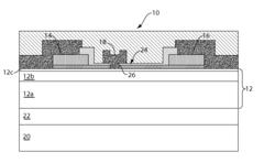
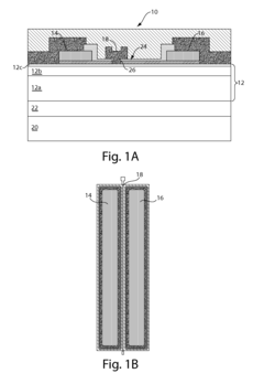
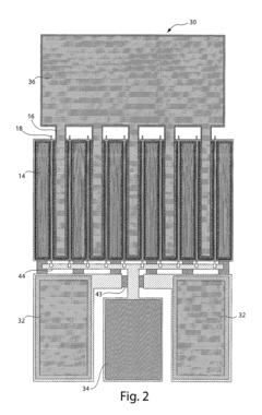
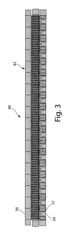
Passivation layers are critical for protecting GaN transistors from environmental factors and enhancing their longevity. These layers typically consist of dielectric materials such as silicon nitride (SiN), silicon dioxide (SiO2), or aluminum oxide (Al2O3) that are deposited on the surface of the transistor. The passivation layer helps to reduce surface states, prevent current collapse, and protect against moisture and contaminants, thereby improving device reliability and extending operational lifetime.- Passivation layers for GaN transistors: Passivation layers are critical for protecting GaN transistors from environmental factors and enhancing their longevity. These layers typically consist of dielectric materials such as silicon nitride, silicon dioxide, or aluminum oxide that are deposited on the surface of the transistor. The passivation layer prevents surface states and traps that can degrade device performance over time, reduces current collapse phenomena, and improves reliability under high-voltage operation. Proper passivation techniques can significantly extend the operational lifetime of GaN transistors by mitigating electron trapping and surface-related degradation mechanisms.
- Metal encapsulation and barrier coatings: Metal encapsulation and barrier coatings provide enhanced protection for GaN transistors against moisture, oxygen, and other contaminants that can accelerate device degradation. These coatings typically consist of metals or metal compounds such as titanium, aluminum, gold, or platinum that form a hermetic seal around the device. The barrier properties prevent ion migration and chemical reactions at the semiconductor interfaces. Advanced multi-layer metal stacks can be designed to address specific environmental challenges while maintaining electrical performance. These coatings are particularly important for GaN transistors operating in harsh environments or high-temperature applications where conventional packaging may be insufficient.
- Thermal management coatings: Thermal management coatings are specialized materials applied to GaN transistors to improve heat dissipation and prevent thermal degradation. These coatings typically have high thermal conductivity and can include diamond-like carbon, aluminum nitride, or metal-ceramic composites. By efficiently transferring heat away from the active device regions, these coatings prevent hot spots that accelerate device aging and failure mechanisms. The thermal management approach often involves multiple layers with different thermal properties to optimize both heat spreading and dissipation. Effective thermal management through specialized coatings can significantly extend the operational lifetime of GaN transistors, particularly in high-power applications.
- Surface treatment and interface engineering: Surface treatment and interface engineering techniques are employed to enhance the longevity of GaN transistors by modifying the semiconductor surface before coating application. These processes include chemical cleaning, plasma treatment, and atomic layer deposition to remove contaminants and create optimal interfaces between the GaN and coating materials. Proper interface engineering reduces defect density and prevents delamination of protective coatings during thermal cycling. Surface treatments can also passivate dangling bonds and reduce interface states that contribute to device degradation. These techniques are critical for ensuring strong adhesion between the GaN surface and subsequent coating layers, thereby improving long-term reliability.
- Composite and nanostructured protective coatings: Advanced composite and nanostructured coatings represent the cutting edge in GaN transistor protection technology. These coatings combine multiple materials at the nanoscale to achieve superior protective properties that cannot be obtained from single-material approaches. Examples include nanocomposites of ceramics and polymers, self-healing materials that can repair microcracks, and gradient-structured coatings that provide a smooth transition between dissimilar materials. Nanostructured coatings can be tailored to address specific degradation mechanisms while maintaining electrical performance. The controlled architecture of these advanced coatings provides enhanced resistance to mechanical stress, thermal cycling, and electrical field-induced degradation, significantly extending the operational lifetime of GaN transistors.
02 Encapsulation materials for thermal management
Specialized encapsulation materials are used to enhance thermal management in GaN transistors, which is crucial for their longevity. These materials include thermally conductive polymers, ceramic-filled epoxies, and metal-based composites that efficiently dissipate heat generated during operation. Proper thermal management prevents degradation due to high operating temperatures, reduces thermal stress at material interfaces, and maintains stable electrical performance over time, significantly extending the transistor's operational life.Expand Specific Solutions03 Surface treatments and buffer layers
Surface treatments and buffer layers play a vital role in improving the interface quality between GaN and substrate materials, enhancing transistor longevity. Techniques such as plasma treatment, chemical cleaning, and the deposition of nucleation layers help reduce defect density and strain at interfaces. Buffer layers composed of materials like AlN or AlGaN create a gradual transition between the substrate and active GaN layer, minimizing lattice mismatch and preventing the propagation of dislocations that could lead to device failure over time.Expand Specific Solutions04 Metal contact and gate engineering
Advanced metal contact and gate engineering techniques are employed to enhance the reliability and longevity of GaN transistors. This includes using multi-layer metal stacks with diffusion barriers, specialized annealing processes, and field plate structures to optimize current distribution and reduce electric field crowding. Gate dielectrics with high thermal stability and resistance to ion migration help prevent threshold voltage shifts and gate leakage over time, while carefully designed ohmic contacts minimize contact resistance degradation during operation.Expand Specific Solutions05 Protective coatings against environmental factors
Environmental protective coatings are applied to GaN transistors to shield them from moisture, oxygen, and other corrosive elements that can degrade performance over time. These coatings typically consist of hermetic sealing materials, conformal polymers, or inorganic films that provide a barrier against environmental contaminants. Some advanced coatings incorporate self-healing properties or getter materials that can absorb harmful gases within the package, further extending device lifetime by maintaining a controlled internal environment throughout the operational life of the transistor.Expand Specific Solutions
Leading Companies in GaN Coating Solutions
The gallium nitride (GaN) transistor coating materials market is currently in a growth phase, characterized by increasing adoption across power electronics, telecommunications, and automotive sectors. The market is projected to expand significantly due to GaN's superior performance in high-power, high-frequency applications. Leading semiconductor manufacturers like TSMC, Intel, and Samsung Electronics are investing heavily in GaN technology development, while specialized players such as GaN Systems and MACOM Technology Solutions are focusing on innovative coating solutions to enhance transistor longevity. Research institutions including Tohoku University and CEA are advancing fundamental materials science in this area. The competitive landscape features both established semiconductor giants and niche players developing proprietary coating technologies to address thermal management, electrical stability, and environmental protection challenges for GaN transistors.
GaN Systems, Inc.
Technical Solution: GaN Systems has developed proprietary Island Technology® coating architecture for GaN transistors that incorporates specialized dielectric layers and passivation techniques. Their approach uses a multi-layer coating system with silicon nitride (SiN) as the primary passivation layer, combined with field plate structures to manage electric field distribution. The company employs atomic layer deposition (ALD) techniques to create uniform, defect-free interfaces between GaN and dielectric materials. Their latest generation coatings incorporate stress-compensation layers that minimize mechanical strain during thermal cycling, significantly reducing delamination risks. GaN Systems' coating technology also features specialized edge termination structures that prevent premature breakdown at device peripheries, extending operational lifetime by up to 10x compared to conventional designs.
Strengths: Superior thermal management capabilities, excellent protection against moisture and contaminants, and field-proven reliability in automotive applications. Weaknesses: Higher manufacturing costs compared to traditional solutions, and requires specialized deposition equipment that limits production scalability.
Taiwan Semiconductor Manufacturing Co., Ltd.
Technical Solution: TSMC has pioneered advanced coating solutions for GaN transistors through their GaN-on-Si technology platform. Their approach utilizes a sophisticated multi-layer coating system featuring alternating layers of silicon nitride and silicon oxide deposited through plasma-enhanced chemical vapor deposition (PECVD). This creates a stress-balanced structure that minimizes lattice mismatch issues. TSMC's proprietary surface treatment process before coating application significantly reduces interface states and trapping effects. Their coating technology incorporates specialized transition layers between GaN and passivation materials to manage differences in thermal expansion coefficients. TSMC has also developed high-k dielectric integration techniques for their GaN devices, allowing for enhanced channel control while maintaining surface protection. Recent advancements include carbon-doped buffer layers that improve isolation and reduce leakage currents in high-voltage applications.
Strengths: Industry-leading process control and uniformity, excellent scalability for mass production, and comprehensive reliability testing infrastructure. Weaknesses: Higher cost structure compared to specialized GaN foundries, and somewhat conservative approach to implementing cutting-edge materials.
Critical Patents and Research in GaN Protection
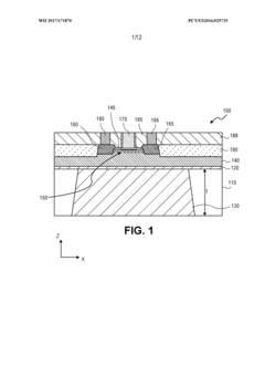
Gallium nitride transistor with underfill aluminum nitride for improved thermal and RF performance
PatentWO2017171870A1
Innovation
- Incorporating an aluminum nitride layer under the gallium nitride transistor or circuit block, utilizing a low resistivity silicon substrate, which provides both high thermal conductivity and high resistivity through the aluminum nitride's insulating properties and superior thermal conductivity compared to silicon.
Gallium nitride material transistors and methods associated with the same
PatentInactiveUS20100019850A1
Innovation
- The development of gallium nitride material transistors with active regions formed in gallium nitride layers, integrated with a matching circuit to transform impedance, enabling the amplification of input signals to produce output signals with an adjacent channel power ratio (ACPR) of less than or equal to −20 dBc, while maintaining high drain efficiencies and output powers.
Environmental Impact of Coating Materials
The environmental impact of coating materials used in gallium nitride (GaN) transistor manufacturing and operation represents a critical consideration in the sustainable development of this technology. Traditional coating materials often contain heavy metals, volatile organic compounds (VOCs), and other potentially hazardous substances that pose significant environmental risks throughout their lifecycle. The manufacturing processes for these coatings frequently require substantial energy inputs and generate considerable waste streams that may contaminate soil and water systems if not properly managed.
Recent advancements in eco-friendly coating alternatives show promising developments. Silicon dioxide (SiO2) and silicon nitride (Si3N4) based coatings offer reduced environmental footprints compared to conventional materials, with lower toxicity profiles and improved recyclability characteristics. Additionally, carbon-based coatings such as diamond-like carbon (DLC) demonstrate excellent durability while minimizing environmental impact during production and disposal phases.
Life cycle assessment (LCA) studies indicate that the environmental burden of coating materials extends beyond manufacturing to include operational and end-of-life stages. During operation, some coating materials may gradually degrade, potentially releasing particulates into the environment. The thermal cycling experienced by GaN transistors can accelerate this degradation process, particularly in harsh operating environments such as automotive or industrial applications.
Regulatory frameworks worldwide are increasingly addressing the environmental aspects of electronic components. The European Union's Restriction of Hazardous Substances (RoHS) directive and Registration, Evaluation, Authorization and Restriction of Chemicals (REACH) regulations have significant implications for coating material selection. Similarly, the United States Environmental Protection Agency (EPA) has established guidelines that influence coating material choices for semiconductor applications.
Emerging sustainable coating technologies include bio-based polymers and water-based coating systems that substantially reduce environmental impact. These innovations aim to maintain or enhance the protective properties of coatings while minimizing ecological footprints. Research indicates that plant-derived polymers can provide comparable protection to synthetic alternatives while offering improved biodegradability characteristics.
The recyclability and end-of-life management of coated GaN transistors present ongoing challenges. Current recycling technologies often struggle to effectively separate coating materials from semiconductor substrates, resulting in downcycling rather than true recycling. Innovative approaches such as design-for-disassembly and solvent-based coating removal techniques show promise for improving the circularity of these components in the future.
Reliability Testing Standards for Coated GaN Devices
Reliability testing standards for coated GaN devices must adhere to rigorous protocols to ensure performance consistency and longevity under various operational conditions. The Joint Electron Device Engineering Council (JEDEC) has established several standards specifically applicable to GaN transistors, including JESD22-A108 for temperature cycling, JESD22-A110 for highly accelerated temperature and humidity stress testing, and JESD47 for stress-test-driven qualification of integrated circuits.
For coated GaN devices, the IEC 60749 series provides comprehensive testing methodologies that evaluate the effectiveness of protective coatings against environmental stressors. These standards incorporate high-temperature operating life (HTOL) tests typically conducted at 150°C for 1000 hours, which are essential for assessing the thermal stability of coating materials and their interface with GaN substrates.
The automotive industry, through the AEC-Q101 qualification requirements, imposes additional testing rigor for GaN devices intended for vehicular applications. These standards mandate humidity-temperature-bias (HTB) testing at 85°C/85% relative humidity for at least 1000 hours, which is particularly relevant for evaluating coating hydrophobicity and moisture barrier properties.
Military and aerospace applications follow MIL-STD-750 and MIL-STD-883 standards, which include salt fog testing (Method 1009) and mixed flowing gas testing to simulate corrosive environments. These tests are critical for determining coating resistance to chemical degradation and ion migration that could compromise device performance.
Recent developments in reliability testing have introduced power cycling tests that simulate real-world operational conditions. These tests typically involve cycling between temperature extremes (-40°C to 150°C) while the device is under electrical load, providing insights into thermomechanical stress effects on coating adhesion and integrity over time.
Radiation hardness testing, following ASTM F1892 guidelines, has become increasingly important for GaN devices deployed in space applications or radiation-intensive environments. Coatings must demonstrate stability under total ionizing dose (TID) exposure, typically up to 300 krad(Si), without significant degradation of electrical parameters.
The emerging trend toward standardized accelerated life testing (ALT) protocols specifically designed for wide-bandgap semiconductors represents a significant advancement in reliability assessment. These protocols typically combine multiple stressors—temperature, humidity, electrical bias, and mechanical stress—to provide more realistic predictions of long-term coating performance in field conditions.
Unlock deeper insights with Patsnap Eureka Quick Research — get a full tech report to explore trends and direct your research. Try now!
Generate Your Research Report Instantly with AI Agent
Supercharge your innovation with Patsnap Eureka AI Agent Platform!