

Material Selection in Gallium Nitride Transistor Fabrication Processes
OCT 14, 202510 MIN READ
Generate Your Research Report Instantly with AI Agent
PatSnap Eureka helps you evaluate technical feasibility & market potential.
GaN Transistor Development Background and Objectives
Gallium Nitride (GaN) transistor technology has emerged as a revolutionary advancement in the field of power electronics and high-frequency applications. The evolution of GaN transistors began in the early 1990s when researchers first recognized the potential of wide bandgap semiconductors for electronic devices. Unlike conventional silicon-based transistors, GaN offers superior electron mobility, higher breakdown voltage, and enhanced thermal conductivity, making it exceptionally suitable for high-power and high-frequency applications.
The technological trajectory of GaN transistors has been marked by significant milestones, including the development of Metal-Organic Chemical Vapor Deposition (MOCVD) techniques for high-quality GaN epitaxial growth, the innovation of AlGaN/GaN heterostructures, and the creation of effective passivation methods to mitigate surface-related issues. These advancements have collectively propelled GaN transistor technology from laboratory curiosity to commercial viability over the past three decades.
Material selection in GaN transistor fabrication represents a critical aspect of the manufacturing process, directly influencing device performance, reliability, and cost-effectiveness. The primary materials involved include the GaN epitaxial layer, buffer layers, barrier layers (typically AlGaN), gate metals, ohmic contacts, passivation materials, and substrate materials such as silicon, silicon carbide, or sapphire. Each material choice presents unique trade-offs between performance parameters, manufacturing complexity, and economic considerations.
The current technological objectives in GaN transistor development focus on several key areas. First, enhancing material quality through defect reduction and improved epitaxial growth techniques to maximize electron mobility and minimize leakage currents. Second, optimizing interface properties between different material layers to reduce interface trapping effects that degrade device performance. Third, developing novel material combinations and structures to push the boundaries of operating frequency, power handling capability, and efficiency.
Looking forward, the field aims to achieve significant breakthroughs in material integration, particularly in areas such as gate stack engineering, advanced barrier layer designs, and innovative substrate solutions. The ultimate goal is to develop GaN transistors that can operate reliably at higher voltages (>1200V), higher frequencies (>100 GHz), and higher temperatures (>250°C) while maintaining cost-competitiveness with silicon-based alternatives.
The material selection challenges in GaN transistor fabrication must be addressed within the context of scalable manufacturing processes, as the industry transitions from specialized applications to mass-market adoption in automotive, renewable energy, and consumer electronics sectors. This transition necessitates not only performance optimization but also material choices that enable high-yield, reproducible manufacturing processes suitable for high-volume production environments.
Market Analysis for GaN Power Electronics
The global market for Gallium Nitride (GaN) power electronics has experienced remarkable growth in recent years, driven by increasing demand for high-efficiency power conversion systems across multiple industries. Current market valuations place the GaN power device sector at approximately 1.4 billion USD in 2023, with projections indicating a compound annual growth rate (CAGR) of 25-30% through 2030, potentially reaching 6.5 billion USD by the end of the decade.
Consumer electronics represents the largest application segment, accounting for roughly 35% of the total market share. This dominance stems from the adoption of GaN-based fast chargers for smartphones, laptops, and other portable devices, where the material's superior power density enables smaller form factors and faster charging capabilities compared to silicon alternatives.
The automotive sector follows closely as the second-largest market segment, currently representing about 28% of GaN power electronics applications. Electric vehicle manufacturers are increasingly incorporating GaN transistors in onboard chargers, DC-DC converters, and inverters to improve power conversion efficiency, reduce thermal management requirements, and decrease overall vehicle weight. Industry forecasts suggest this segment will experience the fastest growth rate, potentially overtaking consumer electronics by 2027.
Industrial power systems constitute approximately 20% of the current market, with applications in motor drives, uninterruptible power supplies, and renewable energy conversion systems. The telecommunications sector accounts for 12% of market share, primarily in base station power supplies and RF amplifiers where GaN's high-frequency performance offers significant advantages.
Regionally, Asia-Pacific dominates the market with approximately 45% share, driven by the strong presence of semiconductor manufacturing facilities and consumer electronics production in countries like Japan, South Korea, Taiwan, and increasingly China. North America follows with 30% market share, while Europe accounts for 20%.
The competitive landscape features both established semiconductor giants and specialized GaN technology companies. Key market players include Infineon Technologies, Texas Instruments, GaN Systems (now part of Infineon), Efficient Power Conversion (EPC), Transphorm, and Navitas Semiconductor. These companies are engaged in continuous material innovation and manufacturing process improvements to address challenges in material selection for GaN transistor fabrication.
Market barriers include relatively higher production costs compared to silicon devices, supply chain constraints for high-quality GaN substrates, and technical challenges related to material defects and reliability. However, as manufacturing scales and fabrication processes mature, the price premium for GaN devices is steadily decreasing, accelerating market penetration across all application segments.
Current Material Challenges in GaN Transistor Fabrication
Despite significant advancements in GaN transistor technology, material-related challenges continue to impede optimal device performance and manufacturing efficiency. The substrate material selection remains a critical challenge, with sapphire, silicon carbide (SiC), and silicon each presenting distinct trade-offs. Sapphire substrates offer excellent insulating properties but suffer from poor thermal conductivity and lattice mismatch with GaN. SiC provides superior thermal management and closer lattice matching but at significantly higher costs. Silicon substrates, while economically attractive and compatible with existing semiconductor infrastructure, introduce substantial challenges in managing stress due to thermal expansion coefficient differences.
Buffer layer materials present another significant hurdle, as they must effectively mitigate lattice mismatch between GaN and the substrate. Current AlN and AlGaN buffer solutions often contain high densities of threading dislocations that propagate into the active device regions, degrading electrical performance and reliability. The optimization of buffer layer composition, thickness, and growth conditions remains an active area of research with considerable room for improvement.
Gate dielectric materials pose particular challenges for enhancement-mode GaN transistors. Traditional materials like SiO2 and Si3N4 exhibit interface quality issues when deposited on GaN, resulting in threshold voltage instability and reduced channel mobility. High-k dielectrics such as Al2O3 and HfO2 show promise but still struggle with interface trap densities and long-term reliability under high-field conditions.
Ohmic contact formation represents another persistent material challenge. The conventional Ti/Al/Ni/Au metallization scheme requires high-temperature annealing that can degrade other device structures. Additionally, achieving consistently low contact resistance while maintaining smooth morphology remains difficult, particularly for p-GaN contacts where the wide bandgap and limited p-type doping efficiency create inherent barriers to forming low-resistance contacts.
Passivation materials used to protect device surfaces and reduce current collapse phenomena face durability issues under high-temperature and high-field operation. Current SiN and Al2O3 passivation layers often exhibit degradation over time, leading to reliability concerns in high-power applications. The interface between these passivation materials and GaN frequently contains charge trapping sites that contribute to dynamic Ron issues and current collapse.
Heat dissipation materials and thermal management solutions represent a growing challenge as power densities increase. The thermal boundary resistance between GaN and various substrate and packaging materials limits effective heat extraction, while advanced thermal interface materials often lack the necessary reliability for long-term operation in harsh environments.
Current Material Selection Approaches for GaN Devices
01 Substrate materials for GaN transistors
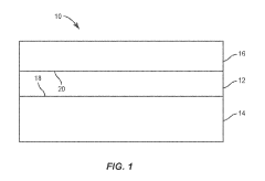
Various substrate materials can be used for growing gallium nitride (GaN) layers for transistor applications. Silicon carbide (SiC) substrates offer excellent thermal conductivity and lattice matching with GaN, making them ideal for high-power applications. Silicon substrates provide cost advantages and integration possibilities with existing silicon-based technologies. Sapphire substrates are also commonly used despite lattice mismatch issues. The choice of substrate material significantly impacts the performance, thermal management, and cost of GaN transistors.- Substrate materials for GaN transistors: The choice of substrate material is critical for gallium nitride transistor performance. Common substrates include silicon carbide (SiC), sapphire, and silicon. SiC substrates offer superior thermal conductivity and lattice matching with GaN, resulting in better device performance for high-power applications. Sapphire substrates are used for their transparency and insulating properties, while silicon substrates provide cost advantages and integration with existing semiconductor manufacturing processes.
- Buffer and transition layers: Buffer and transition layers are essential in GaN transistor fabrication to manage lattice mismatch between GaN and the substrate material. These layers, often composed of AlN, AlGaN, or graded compositions, help reduce defect density and improve crystal quality. Properly designed buffer layers minimize stress, prevent cracking, and enhance electron mobility in the active region, resulting in improved device performance and reliability.
- Channel and barrier layer materials: The selection of channel and barrier layer materials significantly impacts GaN transistor performance. AlGaN/GaN heterostructures are commonly used, where the aluminum content in the AlGaN barrier layer determines the band offset and carrier concentration. Alternative barrier materials include InAlN and AlInGaN, which can provide better lattice matching and higher carrier density. The channel layer composition and thickness affect electron mobility, current capacity, and breakdown voltage.
- Contact and metallization materials: Contact and metallization materials are crucial for achieving low-resistance ohmic contacts and reliable Schottky contacts in GaN transistors. For ohmic contacts, multi-layer metal stacks containing Ti/Al/Ni/Au or Ti/Al/Ti/Au are commonly used. Schottky gate contacts often utilize Ni/Au, Pt/Au, or Pd/Au. The selection of these materials and their deposition processes significantly impacts device performance, reliability, and thermal stability under high-power operation.
- Passivation and encapsulation materials: Passivation and encapsulation materials protect GaN transistors from environmental factors and enhance device stability. Silicon nitride (SiN), silicon dioxide (SiO2), and aluminum oxide (Al2O3) are commonly used for surface passivation to reduce current collapse and improve reliability. These materials help mitigate surface-related trapping effects and protect against moisture and contaminants. Advanced passivation schemes may incorporate multiple layers or novel materials to optimize device performance and longevity.
02 Buffer and transition layers for GaN devices
Buffer and transition layers play a crucial role in GaN transistor fabrication by managing lattice mismatch between the substrate and active GaN layers. These layers typically include AlN, AlGaN, or graded composition layers that help reduce defect density and improve crystal quality. Properly designed buffer layers minimize strain, prevent cracking, and enhance electron mobility in the device. Advanced buffer layer architectures can include multiple layers with varying compositions to gradually transition from the substrate to the active GaN region.Expand Specific Solutions03 Barrier layer materials and compositions
The barrier layer in GaN transistors, typically composed of AlGaN, creates a two-dimensional electron gas (2DEG) at the interface with GaN through polarization effects. The aluminum content in the AlGaN barrier layer affects the sheet carrier concentration and threshold voltage of the device. Alternative barrier materials include InAlN, AlN, and AlInGaN, each offering different advantages in terms of lattice matching, carrier confinement, and device performance. The thickness and composition of these barrier layers are critical parameters that determine the electrical characteristics of GaN transistors.Expand Specific Solutions04 Channel and active region materials
The channel region in GaN transistors is where current flows between the source and drain terminals. High-purity GaN is typically used for the channel, but modifications such as InGaN channels can enhance electron mobility. The quality of the channel material directly impacts device performance metrics like on-resistance and maximum current density. Advanced designs may incorporate channel engineering techniques such as polarization doping or the introduction of quantum wells to optimize carrier transport properties and improve device efficiency.Expand Specific Solutions05 Passivation and protection materials
Surface passivation layers are essential for protecting GaN transistors from environmental degradation and for stabilizing device performance. Materials such as silicon nitride (SiN), silicon dioxide (SiO2), and aluminum oxide (Al2O3) are commonly used for passivation. These materials help reduce surface states, prevent current collapse, and improve reliability. The passivation layer thickness and deposition method significantly affect device characteristics. Advanced passivation schemes may employ multiple dielectric layers or in-situ passivation techniques to minimize interface traps and enhance long-term stability.Expand Specific Solutions
Leading Companies in GaN Transistor Manufacturing
The gallium nitride (GaN) transistor fabrication market is currently in a growth phase, with an estimated market size exceeding $1.5 billion and projected to expand at a CAGR of 20% through 2027. The competitive landscape features established semiconductor giants like Texas Instruments, Intel, and TSMC alongside GaN specialists such as GaN Systems, Efficient Power Conversion, and MACOM Technology Solutions. Technical maturity varies significantly across players, with companies like Infineon, Samsung, and Huawei demonstrating advanced capabilities in material selection processes. Academic-industry partnerships are accelerating innovation, particularly with institutions like Xidian University and Taiyuan University of Technology collaborating with commercial entities. The market is characterized by regional clusters of expertise in North America, East Asia, and Europe, with companies competing to optimize material selection for enhanced performance, reliability, and cost-effectiveness in power electronics applications.
GaN Systems, Inc.
Technical Solution: GaN Systems has pioneered advanced material selection techniques for GaN transistor fabrication, focusing on their patented Island Technology® that uses a unique die design to optimize thermal performance and reliability. Their approach incorporates high-purity GaN epitaxial layers grown on silicon carbide (SiC) substrates to maximize electron mobility while minimizing defects. The company has developed proprietary surface passivation techniques using optimized dielectric materials that significantly reduce current collapse and dynamic RDS(on) degradation. Their fabrication process includes specialized buffer layer architectures that manage lattice mismatch between GaN and substrate materials, reducing dislocation densities to below 10^8 cm^-2. GaN Systems also employs advanced metal stack configurations for ohmic contacts, utilizing Ti/Al/Ni/Au multilayers with precise thickness ratios and annealing profiles to achieve contact resistances below 0.5 Ω·mm.
Strengths: Superior thermal management through Island Technology enables higher power density; SiC substrate integration provides excellent thermal conductivity and reduced lattice mismatch. Weaknesses: Higher manufacturing costs compared to silicon-based alternatives; challenges in scaling production while maintaining consistent material quality across large wafers.
INFINEON TECHNOLOGIES AMERICAS CORP
Technical Solution: Infineon has developed a comprehensive material selection strategy for GaN transistor fabrication centered around their CoolGaN™ technology. Their approach utilizes a sophisticated GaN-on-Si epitaxial growth process with carefully engineered transition layers to accommodate the 17% lattice mismatch and 54% thermal expansion coefficient difference between GaN and silicon. The company employs proprietary in-situ SiN passivation techniques during MOCVD growth, which significantly reduces surface states and enhances device reliability. Infineon's material stack includes optimized AlGaN barrier layers with precisely controlled aluminum content (typically 20-25%) and thickness (20-25nm) to maximize 2DEG density while preventing parasitic conduction. Their fabrication process incorporates specialized carbon-doped GaN buffer layers that achieve high breakdown voltages (>600V) while maintaining low leakage currents (<1μA/mm²). Additionally, Infineon utilizes advanced gate dielectric materials with high-k properties to minimize gate leakage while enabling enhancement-mode operation.
Strengths: Cost-effective GaN-on-Si approach enables manufacturing in existing 200mm silicon fabs; excellent reliability with failure rates below 1 FIT. Weaknesses: Silicon substrate limits thermal performance compared to SiC alternatives; epitaxial quality challenges at layer thicknesses required for higher voltage applications (>900V).
Critical Materials Science Innovations for GaN Transistors
Gallium nitride material structures including substrates and methods associated with the same
PatentInactiveUS7791106B2
Innovation
- A composite substrate with a thin silicon surface layer and a strain-absorbing layer is used to reduce stress, incorporating a transition layer to promote favorable strain conditions, minimizing defect formation and warping, and enabling high-quality gallium nitride material growth on substrates with diameters of at least 100 mm and thicknesses greater than 2 microns.
Gallium nitride materials and methods
PatentInactiveUS20200243651A9
Innovation
- A compositionally-graded transition layer is introduced between the silicon substrate and the gallium nitride material layer to alleviate stress, reducing the likelihood of cracking and defects by matching thermal expansion rates and providing strain relief.
Substrate Alternatives and Their Impact on GaN Performance
The selection of substrate materials represents a critical decision point in GaN transistor fabrication, directly influencing device performance, reliability, and cost-effectiveness. Traditional GaN epitaxial growth has predominantly relied on sapphire substrates due to their thermal stability and commercial availability. However, the significant lattice mismatch between sapphire and GaN (approximately 16%) introduces high dislocation densities that compromise electron mobility and device efficiency.
Silicon carbide (SiC) has emerged as a premium alternative substrate, offering superior thermal conductivity (3.7 W/cm·K compared to sapphire's 0.3 W/cm·K) and a reduced lattice mismatch of only 3.5%. These properties enable GaN-on-SiC devices to handle significantly higher power densities and operate at elevated temperatures with improved reliability. The enhanced heat dissipation capabilities of SiC substrates have made them the preferred choice for high-frequency RF applications and power electronics despite their higher cost structure.
Silicon substrates represent the most economically attractive alternative, potentially reducing manufacturing costs by 60-70% compared to SiC-based solutions. The integration of GaN-on-Si technology with established silicon manufacturing infrastructure presents compelling economies of scale. However, the 17% lattice mismatch and 56% thermal expansion coefficient difference between Si and GaN necessitate complex buffer layer architectures to mitigate stress and prevent wafer bowing during the cooling phase of epitaxial growth.
Recent advancements in buffer layer engineering have significantly improved GaN-on-Si performance metrics. Sophisticated AlN/AlGaN transition layers with carefully controlled composition gradients have reduced dislocation densities from 10^10 cm^-2 to approximately 10^8 cm^-2, approaching the quality levels achieved with more expensive substrates.
Diamond substrates represent the frontier of GaN substrate technology, offering unprecedented thermal conductivity exceeding 20 W/cm·K. Laboratory demonstrations have shown that GaN-on-diamond devices can operate at power densities 3-5 times higher than conventional alternatives. However, commercialization remains limited by prohibitive costs and technical challenges in achieving uniform GaN epitaxial growth on diamond surfaces.
Bulk GaN substrates, though ideal from a lattice matching perspective, continue to face manufacturing constraints that limit their widespread adoption. Current production methods yield relatively small diameter wafers (typically 2-4 inches) at costs approximately 8-10 times higher than SiC alternatives. Nevertheless, for specialized applications requiring ultimate performance, native GaN substrates deliver unmatched electron mobility and breakdown voltage characteristics.
The substrate selection ultimately involves balancing performance requirements against economic constraints, with different industries prioritizing distinct aspects of this trade-off. The telecommunications sector generally favors SiC-based solutions for RF applications, while consumer electronics and automotive applications increasingly leverage the cost advantages of GaN-on-Si technology as buffer layer engineering continues to advance.
Environmental Considerations in GaN Material Processing
The environmental impact of Gallium Nitride (GaN) material processing has become increasingly significant as the semiconductor industry expands its adoption of this wide bandgap material. GaN transistor fabrication involves several processes that require careful environmental consideration, particularly regarding resource consumption, waste generation, and energy usage.
Manufacturing GaN-based devices typically requires substantial water resources for cleaning and processing steps. Compared to traditional silicon processing, GaN fabrication can consume 20-30% more ultra-pure water, presenting challenges in regions facing water scarcity. Additionally, the chemical mechanical polishing (CMP) processes used in GaN substrate preparation generate wastewater containing suspended GaN particles and chemical compounds that require specialized treatment before discharge.
Energy consumption represents another critical environmental concern. The high-temperature conditions necessary for GaN epitaxial growth—often exceeding 1000°C—demand significant energy inputs. Metal-organic chemical vapor deposition (MOCVD), the predominant method for growing high-quality GaN layers, operates at elevated temperatures for extended periods, contributing substantially to the carbon footprint of GaN device manufacturing.
The precursor materials used in GaN processing present unique environmental challenges. Trimethylgallium (TMGa) and ammonia, commonly used in MOCVD processes, are hazardous substances requiring careful handling and disposal protocols. Unreacted precursors and byproducts must undergo thermal or chemical treatment to neutralize their environmental impact, adding complexity to waste management systems in fabrication facilities.
Recent advancements in GaN processing technologies have begun addressing these environmental concerns. Improved MOCVD reactor designs have enhanced precursor utilization efficiency by 15-25%, reducing waste generation and energy consumption. Closed-loop water recycling systems implemented by leading manufacturers have demonstrated potential water usage reductions of up to 40% in GaN fabrication lines.
The industry has also explored alternative substrate materials to reduce the environmental burden. Silicon carbide (SiC) substrates, while more expensive than silicon, offer improved thermal conductivity that can reduce cooling requirements during device operation. Meanwhile, innovative approaches using nanoporous GaN templates have shown promise in reducing material consumption while maintaining device performance characteristics.
Regulatory frameworks worldwide are increasingly focusing on the environmental aspects of semiconductor manufacturing, including GaN processing. The European Union's Restriction of Hazardous Substances (RoHS) directive and similar regulations in other regions have prompted manufacturers to develop more environmentally sustainable GaN fabrication methods, driving innovation in green processing technologies.
Unlock deeper insights with PatSnap Eureka Quick Research — get a full tech report to explore trends and direct your research. Try now!
Generate Your Research Report Instantly with AI Agent
Supercharge your innovation with PatSnap Eureka AI Agent Platform!