Understanding Patent Dynamics in Gallium Nitride Transistor Technologies
OCT 14, 202510 MIN READ
Generate Your Research Report Instantly with AI Agent
Patsnap Eureka helps you evaluate technical feasibility & market potential.
GaN Transistor Evolution and Research Objectives
Gallium Nitride (GaN) transistor technology has emerged as a revolutionary advancement in the semiconductor industry over the past three decades. The evolution of GaN transistors began in the early 1990s with fundamental research into wide bandgap semiconductors, driven by the limitations of silicon-based devices in high-power, high-frequency applications. The inherent properties of GaN, including its wide bandgap (3.4 eV), high electron mobility, and superior thermal conductivity, positioned it as an ideal candidate for next-generation electronic devices.
The technological trajectory of GaN transistors has been marked by several significant milestones. Initial development focused on overcoming material growth challenges, particularly the lack of native substrates. The introduction of Metal-Organic Chemical Vapor Deposition (MOCVD) techniques in the mid-1990s represented a crucial breakthrough, enabling the growth of high-quality GaN epitaxial layers on various substrates such as sapphire, silicon carbide, and silicon.
By the early 2000s, researchers had successfully demonstrated the first high-electron-mobility transistors (HEMTs) based on AlGaN/GaN heterostructures, showcasing unprecedented power density and frequency capabilities. This period also witnessed the emergence of key innovations in device architecture, including field plates for breakdown voltage enhancement and novel buffer layer designs for improved current collapse mitigation.
The primary objective of current GaN transistor research is to address several persistent challenges while expanding application domains. These objectives include enhancing reliability through defect reduction and improved thermal management, increasing operating voltages beyond 1200V for power electronics applications, and pushing frequency capabilities into the millimeter-wave range for advanced communication systems.
Another critical research goal involves cost reduction through substrate innovation and process optimization. The transition from small-diameter SiC substrates to larger, more economical silicon wafers represents a significant focus area, with researchers aiming to overcome the thermal expansion mismatch issues that have historically limited GaN-on-Si performance.
The integration of GaN technology with conventional silicon CMOS processes constitutes another important research direction, potentially enabling monolithic integration of power devices with control circuitry. Additionally, exploration of novel device architectures, such as vertical GaN transistors and GaN-based superjunction structures, aims to push performance boundaries beyond lateral device limitations.
As we look toward future developments, research objectives are increasingly focused on emerging applications in electric vehicles, renewable energy systems, and 5G/6G communication infrastructure, where GaN's unique properties offer substantial advantages over incumbent technologies. The continued evolution of GaN transistor technology promises to revolutionize multiple industries through enhanced energy efficiency, system miniaturization, and performance improvements.
Market Demand Analysis for GaN Power Electronics
The Gallium Nitride (GaN) power electronics market has experienced substantial growth in recent years, driven by increasing demand for high-efficiency power conversion systems across multiple industries. Market research indicates that the global GaN power device market is projected to reach approximately $1.75 billion by 2026, growing at a compound annual growth rate of 33% from 2021. This remarkable growth trajectory reflects the expanding applications of GaN technology in various sectors.
Consumer electronics represents one of the primary demand drivers for GaN power devices. The need for faster charging solutions for smartphones, tablets, and laptops has accelerated the adoption of GaN-based chargers and adapters. These devices offer significantly reduced form factors while delivering higher power outputs compared to traditional silicon-based alternatives. Major smartphone manufacturers have begun incorporating GaN charging technology into their product ecosystems, further stimulating market demand.
The automotive sector presents another substantial market opportunity for GaN power electronics. With the rapid expansion of electric vehicle (EV) production, there is growing demand for more efficient power conversion systems. GaN-based onboard chargers and DC-DC converters can significantly improve power density and efficiency in EVs, extending range capabilities and reducing charging times. Industry forecasts suggest that by 2025, approximately 15% of EV power electronics will incorporate GaN technology.
In the renewable energy sector, GaN power devices are gaining traction for solar inverters and wind power systems. The superior switching characteristics of GaN transistors enable higher frequency operation, resulting in smaller passive components and overall system size reduction. This translates to lower installation costs and improved energy harvest efficiency, critical factors driving adoption in cost-sensitive renewable energy applications.
Telecommunications infrastructure represents another significant market segment for GaN power electronics. The ongoing global deployment of 5G networks requires high-efficiency power amplifiers capable of operating at higher frequencies. GaN-based RF power amplifiers offer superior performance characteristics compared to traditional technologies, making them ideal for next-generation base stations and network infrastructure.
Industrial applications are increasingly adopting GaN technology for motor drives, uninterruptible power supplies, and factory automation systems. The enhanced efficiency and power density of GaN-based solutions directly translate to energy savings and reduced operational costs, compelling value propositions for industrial users facing rising energy prices and sustainability requirements.
Despite the promising market outlook, several factors currently limit wider GaN adoption, including higher component costs compared to silicon alternatives, supply chain constraints, and the need for redesigned power systems to fully leverage GaN capabilities. However, as production volumes increase and manufacturing processes mature, the cost differential is expected to narrow significantly over the next three to five years.
Global GaN Transistor Development Status and Barriers
The global landscape of Gallium Nitride (GaN) transistor technology reveals significant disparities in development status across different regions. Currently, the United States maintains leadership in GaN transistor technology, with major corporations like Cree, Qorvo, and Northrop Grumman possessing advanced manufacturing capabilities and substantial patent portfolios. Japan follows closely, with companies such as Fujitsu, Toshiba, and Panasonic demonstrating strong technological competence, particularly in RF applications. European entities, including STMicroelectronics and Infineon Technologies, have established notable positions in power electronics applications of GaN transistors.
China has been rapidly accelerating its GaN transistor development efforts, with significant investments from both government and private sectors. However, Chinese manufacturers still face challenges in achieving the same level of device performance and reliability as their Western counterparts. South Korea, with Samsung and LG at the forefront, has focused primarily on GaN applications in consumer electronics and display technologies.
Despite the global progress, several critical barriers impede the widespread adoption and advancement of GaN transistor technology. The most significant technical challenge remains the "current collapse" phenomenon, where device performance degrades under high-voltage switching conditions, limiting reliability in power applications. Surface-related trapping effects continue to plague device stability, requiring sophisticated passivation techniques that add complexity to manufacturing processes.
Material quality issues persist, particularly regarding substrate selection. While silicon substrates offer cost advantages, they introduce thermal mismatches and crystal defects that compromise device performance. Native GaN substrates would be ideal but remain prohibitively expensive for mass production. The thermal management of GaN devices presents another substantial challenge, as their high-power density capabilities can lead to localized heating that degrades performance and reliability.
Manufacturing scalability represents a significant barrier to commercialization. Current GaN transistor fabrication processes have not achieved the same level of standardization and yield as silicon technologies, resulting in higher production costs. Additionally, integration challenges with existing silicon-based systems create obstacles for market penetration, as designers must overcome interface issues between different semiconductor technologies.
Regulatory and standardization barriers further complicate global development. The lack of unified standards for GaN transistor performance, reliability testing, and safety certification creates market fragmentation and increases compliance costs for manufacturers operating across multiple regions. These technical and market barriers collectively slow the pace of GaN transistor adoption despite their superior performance characteristics compared to silicon alternatives.
Current GaN Transistor Design Approaches
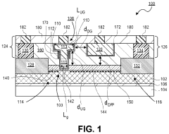
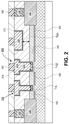
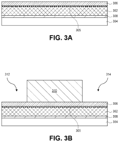
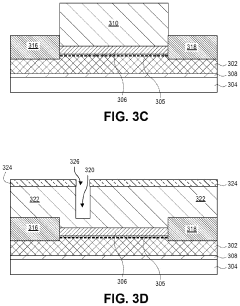
01 Manufacturing processes for GaN transistors
Various manufacturing techniques have been developed for gallium nitride transistors, focusing on improving crystal quality and reducing defects. These processes include specialized epitaxial growth methods, substrate preparation techniques, and post-growth treatments that enhance the electrical properties of the transistors. Advanced fabrication methods help overcome challenges related to lattice mismatch and thermal management, resulting in higher performance devices.- GaN Transistor Fabrication Methods: Various methods for fabricating gallium nitride transistors have been developed to improve performance and reliability. These methods include specialized growth techniques for GaN layers, substrate preparation processes, and novel device architectures. The fabrication approaches focus on reducing defects in the crystal structure and optimizing the interface between different semiconductor layers to enhance electron mobility and device efficiency.
- High Electron Mobility Transistor (HEMT) Designs: Advanced designs for GaN-based High Electron Mobility Transistors have been developed to maximize power handling capabilities and switching speeds. These designs incorporate specialized heterostructures, gate configurations, and channel engineering to optimize the two-dimensional electron gas formation. Innovations in this area focus on reducing parasitic capacitance, minimizing on-resistance, and improving thermal management for high-frequency and high-power applications.
- Substrate and Buffer Layer Technologies: Innovations in substrate materials and buffer layer technologies for GaN transistors address the challenges of lattice mismatch and thermal expansion differences. These technologies include specialized substrate preparation techniques, novel buffer layer compositions, and transition layer structures that reduce defect propagation. The developments aim to improve crystal quality, reduce wafer bow, and enhance overall device reliability while enabling larger wafer sizes for commercial production.
- Power Electronics Applications: GaN transistors have been specifically engineered for power electronics applications, offering advantages in efficiency and power density. These devices feature specialized structures for high breakdown voltage, low switching losses, and enhanced thermal performance. Innovations include field plate designs, edge termination structures, and packaging solutions that enable GaN transistors to outperform silicon-based alternatives in power conversion systems, motor drives, and renewable energy applications.
- Integration and Packaging Technologies: Advanced integration and packaging technologies have been developed to maximize the performance benefits of GaN transistors in practical applications. These include novel die attach methods, interconnect technologies, and thermal management solutions specifically designed for GaN devices. The innovations address challenges related to parasitic inductance, thermal resistance, and electromagnetic interference, enabling higher operating frequencies and power densities in compact form factors.
02 High-frequency and high-power GaN transistor designs
Gallium nitride transistors have been designed specifically for high-frequency and high-power applications. These designs incorporate specialized gate structures, field plates, and channel engineering to handle high voltages and currents while maintaining efficiency. The wide bandgap properties of GaN are leveraged to create transistors that can operate at higher temperatures and frequencies than conventional silicon-based devices, making them ideal for power electronics and RF applications.Expand Specific Solutions03 Substrate innovations for GaN transistor performance
Substrate selection and engineering play crucial roles in GaN transistor performance. Various substrate materials including silicon, silicon carbide, sapphire, and native GaN have been explored to address issues of thermal conductivity, lattice matching, and cost-effectiveness. Techniques such as buffer layers, strain management structures, and novel bonding methods have been developed to improve the quality of GaN growth on these substrates, directly impacting device reliability and performance.Expand Specific Solutions04 Heterostructure and interface engineering in GaN transistors
Advanced heterostructure designs have been implemented in GaN transistors to enhance carrier mobility and confinement. These include AlGaN/GaN, InAlN/GaN, and other compound semiconductor combinations that create two-dimensional electron gas regions with exceptional transport properties. Interface engineering techniques focus on reducing trap states, managing polarization effects, and optimizing band alignments to improve switching speed, reduce leakage currents, and enhance overall device efficiency.Expand Specific Solutions05 Reliability and thermal management solutions
Enhancing the reliability and thermal management of GaN transistors has been a significant focus of patent activity. Innovations include specialized passivation layers, heat dissipation structures, and packaging solutions designed to address the unique challenges of GaN devices. Advanced materials and designs have been developed to mitigate issues such as current collapse, electron trapping, and thermal degradation, extending device lifetime and stability under extreme operating conditions.Expand Specific Solutions
Key Industry Players and Competitive Landscape
The Gallium Nitride (GaN) transistor technology market is currently in a growth phase, with an expanding competitive landscape characterized by both established semiconductor giants and specialized newcomers. Major players like Intel, Texas Instruments, and Taiwan Semiconductor Manufacturing Co. are competing alongside GaN specialists such as Efficient Power Conversion, Transphorm, and Qromis. The market is experiencing rapid development driven by applications in power electronics, RF communications, and automotive sectors, with projected market size reaching several billion dollars by 2025. Technical maturity varies across applications, with companies like MACOM, NXP, and Infineon leading in commercialization efforts, while research institutions including Xidian University and KAUST are advancing fundamental innovations. The competitive dynamics suggest a market transitioning from early adoption to mainstream implementation across multiple industries.
Qromis, Inc.
Technical Solution: Qromis has developed a disruptive GaN-on-QST® (Qromis Substrate Technology) platform that addresses fundamental challenges in GaN power device manufacturing. Their proprietary QST® substrates are engineered with a coefficient of thermal expansion (CTE) closely matched to GaN, enabling the growth of thick, low-defect GaN epitaxial layers on large-diameter wafers (up to 300mm). This approach overcomes the wafer bow and cracking issues that plague conventional GaN-on-Silicon technology. Qromis's platform enables both lateral GaN HEMTs and vertical GaN power devices with breakdown voltages exceeding 1200V. Their technology incorporates advanced field plate designs and channel engineering to optimize the trade-off between breakdown voltage and on-resistance. The QST® platform's superior thermal performance allows for higher current density operation compared to conventional GaN-on-Silicon devices, making it particularly suitable for high-power applications in automotive, industrial, and renewable energy sectors.
Strengths: Superior substrate technology enables larger wafers and higher yield; excellent thermal performance; capability for both lateral and vertical device architectures; potential for very high voltage (>1200V) applications. Weaknesses: Relatively new technology with less field-proven reliability data; higher substrate costs compared to silicon; requires establishment of new manufacturing ecosystem and supply chain.
Efficient Power Conversion Corp.
Technical Solution: EPC has developed an enhancement-mode GaN-on-Silicon technology (eGaN) that creates normally-off transistors without requiring the cascode configuration used by competitors. Their approach features a proprietary gate structure that modifies the threshold voltage to create enhancement-mode operation while maintaining the fundamental advantages of GaN's high electron mobility. EPC's lateral device architecture enables extremely low parasitic capacitances and gate charge, resulting in ultra-fast switching capabilities with transition times in the nanosecond range. Their technology platform has evolved through multiple generations, progressively reducing RDS(on) while increasing current handling capability. EPC has particularly focused on lower voltage applications (40V-200V), where their devices demonstrate significant performance advantages in applications requiring high-frequency operation. The company has pioneered innovative packaging approaches, including chip-scale packaging that minimizes parasitic inductances and enables high-density power designs.
Strengths: True enhancement-mode operation without cascode configuration; industry-leading high-frequency performance; innovative chip-scale packaging minimizes parasitics. Weaknesses: Limited voltage range compared to some competitors (primarily focused below 200V); smaller company with more limited manufacturing scale; chip-scale packaging requires careful board design to manage thermal performance.
Critical Patent Analysis and Technical Innovations
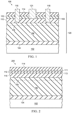
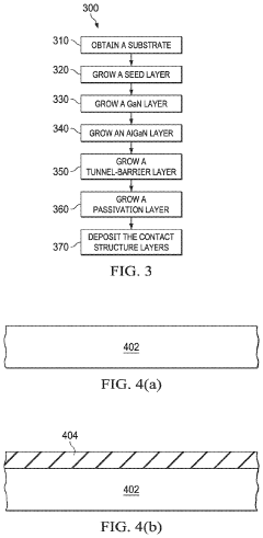
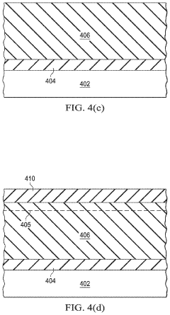
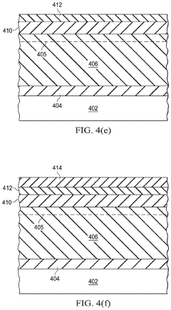
Gallium nitride devices including a tunnel barrier layer
PatentInactiveUS20200203520A1
Innovation
- A modified design assembly for GaN-based transistors includes a tunnel barrier layer with a wide bandgap to prevent electron tunneling to surface traps and states, comprising a substrate, multiple group-III nitride layers, a tunnel barrier layer, and contact structures, which are fabricated using techniques like CVD to ensure effective electron mobility and reduce current collapse.
Gallium nitride (GAN) three-dimensional integrated circuit technology
PatentActiveUS20220102339A1
Innovation
- The integration of gallium nitride (GaN) three-dimensional integrated circuit technology, which includes monolithic 3D integration of GaN NMOS and Si CMOS, enables compact, efficient power delivery and RF solutions by utilizing GaN transistors with drain field plates and multi-gate architectures to enhance breakdown voltage and linearity.
Patent Strategy and IP Portfolio Management
Effective patent strategy for Gallium Nitride (GaN) transistor technologies requires a comprehensive approach to intellectual property management. Companies operating in this high-growth semiconductor segment must develop robust patent portfolios that protect core innovations while enabling strategic market positioning. The patent landscape for GaN transistors has evolved significantly over the past decade, with filing patterns shifting from fundamental materials science to application-specific implementations across power electronics, RF communications, and automotive sectors.
Organizations should implement a multi-layered patent strategy that includes defensive patenting to protect existing product lines, offensive patenting to secure future market opportunities, and strategic licensing to maximize return on R&D investments. For GaN transistor technologies specifically, companies should focus on building patent clusters around critical technology nodes such as epitaxial growth techniques, device structures, packaging solutions, and thermal management approaches.
IP portfolio management for GaN transistors necessitates regular patent landscape analysis to identify white spaces and potential infringement risks. Leading companies typically maintain portfolios with varying patent breadth - combining broad foundational patents with narrower implementation-specific claims. This balanced approach ensures both technological coverage and enforceability in litigation scenarios.
Cross-licensing agreements have become increasingly important in the GaN ecosystem as the technology matures and applications diversify. Companies must carefully evaluate potential licensing partners based on complementary technical capabilities and market access rather than simply patent count. Strategic partnerships with universities and research institutions can also provide cost-effective access to emerging GaN innovations while sharing development risks.
Geographic considerations play a crucial role in GaN patent strategy, with different filing patterns observed across major markets. While the US and Japan historically dominated GaN patent filings, China has emerged as a significant player with rapidly increasing patent activity. Companies should align their filing strategies with both current manufacturing locations and anticipated future markets, particularly as GaN adoption accelerates in electric vehicles and renewable energy applications.
Patent quality metrics should be regularly assessed, focusing not merely on quantity but on strategic alignment with business objectives. Forward citation analysis can help identify the most valuable patents within a GaN portfolio, while claim mapping exercises ensure adequate protection of current and planned product features. Ultimately, successful IP portfolio management for GaN transistor technologies requires close collaboration between technical, legal, and business teams to maintain competitive advantage in this rapidly evolving field.
Standardization and Regulatory Framework
The standardization and regulatory framework for Gallium Nitride (GaN) transistor technologies has evolved significantly over the past decade, reflecting the technology's transition from research laboratories to commercial applications. International bodies such as the International Electrotechnical Commission (IEC) and the Institute of Electrical and Electronics Engineers (IEEE) have developed specific standards addressing the unique characteristics of GaN transistors, particularly focusing on reliability testing methodologies and performance parameters.
The JEDEC Solid State Technology Association has established the JC-70 Wide Bandgap Power Electronic Conversion Semiconductors committee, which has released several guidelines specifically for GaN power devices. These include JEP173: "Dynamic On-Resistance Test Method Guidelines for GaN HEMT Based Power Conversion Devices" and JEP180: "Guideline for Switching Reliability Evaluation Procedures for Gallium Nitride Power Conversion Devices."
Regulatory frameworks vary significantly across different regions, with the European Union implementing the RoHS (Restriction of Hazardous Substances) and REACH (Registration, Evaluation, Authorization and Restriction of Chemicals) directives that impact GaN manufacturing processes. In the United States, the Department of Energy (DOE) and Department of Defense (DoD) have established specific requirements for GaN devices used in power electronics and RF applications for government contracts.
Safety certification requirements present another layer of complexity, with Underwriters Laboratories (UL) and TÜV developing specialized testing protocols for GaN-based power systems. These certifications are crucial for market acceptance in consumer electronics, automotive applications, and industrial power systems.
Patent dynamics in GaN transistor technologies are significantly influenced by these regulatory frameworks, as companies must navigate compliance requirements while protecting their intellectual property. The standardization process itself has become a strategic battlefield where patent holders attempt to influence technical standards to favor their protected technologies.
For emerging applications such as automotive power electronics, additional standards such as AEC-Q101 qualification for discrete semiconductors have been adapted to address the specific characteristics of GaN transistors. These standards establish rigorous reliability and performance requirements that directly impact patent filing strategies and technology development roadmaps.
The interplay between patents and standards creates both opportunities and challenges for market participants. Companies with strong patent portfolios in standardized technologies can leverage their position for licensing revenue, while those developing novel approaches must carefully navigate existing standards to ensure market compatibility while maintaining differentiation.
Unlock deeper insights with Patsnap Eureka Quick Research — get a full tech report to explore trends and direct your research. Try now!
Generate Your Research Report Instantly with AI Agent
Supercharge your innovation with Patsnap Eureka AI Agent Platform!