How Gallium Nitride Transistors Revolutionize High-Power Applications
OCT 14, 20259 MIN READ
Generate Your Research Report Instantly with AI Agent
Patsnap Eureka helps you evaluate technical feasibility & market potential.
GaN Transistor Evolution and Objectives
Gallium Nitride (GaN) transistors represent a significant leap forward in semiconductor technology, emerging as a viable alternative to traditional silicon-based devices. The evolution of GaN transistors began in the early 1990s with fundamental research into wide-bandgap semiconductors, but it wasn't until the early 2000s that practical GaN high-electron-mobility transistors (HEMTs) were developed for commercial applications. This technological progression was driven by increasing demands for higher power density, efficiency, and operating frequencies in electronic systems.
The inherent material properties of GaN provide substantial advantages over silicon. With a bandgap of 3.4 eV compared to silicon's 1.1 eV, GaN can withstand significantly higher electric fields before breakdown. Additionally, GaN's higher electron mobility and saturation velocity enable faster switching speeds and reduced conduction losses, making it particularly suitable for high-power applications.
A critical milestone in GaN transistor development was the introduction of enhancement-mode GaN transistors around 2010, which simplified circuit design by eliminating the need for negative gate bias voltages required by earlier depletion-mode devices. This innovation accelerated adoption across various industries, from power electronics to RF applications.
The technological trajectory of GaN transistors has been characterized by continuous improvements in device structure, substrate materials, and manufacturing processes. Early GaN devices were primarily grown on sapphire or silicon carbide substrates, but cost considerations have driven significant research into GaN-on-silicon technology, which leverages existing silicon manufacturing infrastructure while maintaining acceptable performance characteristics.
Recent advancements have focused on addressing reliability concerns, reducing defect densities, and improving thermal management capabilities. The development of vertical GaN structures represents the latest evolution, promising even higher breakdown voltages and current densities than lateral devices, potentially enabling GaN to penetrate ultra-high-power applications previously dominated by silicon carbide.
The primary objectives of GaN transistor technology development are multifaceted. First, there is a push toward higher operating voltages (>1200V) to expand applications in medium and high-voltage power conversion systems. Second, researchers aim to further reduce on-resistance and switching losses to improve overall system efficiency. Third, enhancing reliability and operational lifetime remains crucial for widespread industrial adoption. Finally, cost reduction through improved manufacturing yields and economies of scale represents a key commercial objective.
Looking forward, GaN transistor technology is expected to continue its evolutionary path with particular emphasis on integration capabilities, enabling monolithic power systems that combine control circuitry with power devices. This integration, coupled with ongoing material improvements, positions GaN transistors as transformative components in the next generation of power electronics, potentially revolutionizing energy conversion across multiple sectors including automotive, renewable energy, and data center infrastructure.
High-Power Applications Market Analysis
The high-power applications market has experienced significant growth in recent years, driven by increasing demand for efficient power management solutions across various industries. The global high-power electronics market was valued at approximately $17.5 billion in 2022 and is projected to reach $28.4 billion by 2028, growing at a CAGR of 8.4% during the forecast period. This growth is primarily fueled by the rapid expansion of electric vehicles, renewable energy systems, and industrial automation.
Electric vehicle adoption represents one of the most substantial market drivers, with global EV sales exceeding 10 million units in 2022, a 55% increase from the previous year. Power electronics, particularly in drivetrain systems and charging infrastructure, constitute a critical component of this market segment. The need for more efficient power conversion and management systems has intensified as manufacturers strive to extend vehicle range and reduce charging times.
The renewable energy sector presents another significant market opportunity for high-power applications. Solar and wind power installations continue to grow globally, with over 290 GW of new renewable capacity added in 2022. These systems require sophisticated power conversion technologies to efficiently integrate with existing grid infrastructure, creating substantial demand for advanced semiconductor solutions.
Data centers represent a third major market segment, with global spending on data center infrastructure reaching $212 billion in 2022. The increasing power density of these facilities, coupled with growing concerns about energy efficiency, has created strong demand for more efficient power delivery architectures. Traditional silicon-based solutions are increasingly struggling to meet these demanding requirements.
Industrial applications, including motor drives, uninterruptible power supplies, and factory automation systems, constitute another substantial market segment. The industrial automation market alone was valued at $191.9 billion in 2021 and is expected to reach $355.4 billion by 2028, with power electronics representing a critical enabling technology for these systems.
Consumer electronics, particularly high-end audio equipment and advanced charging solutions, represent a smaller but rapidly growing segment of the high-power applications market. The demand for faster charging capabilities and more efficient power management in portable devices has created new opportunities for advanced semiconductor technologies.
Across all these segments, there is a clear market trend toward higher efficiency, increased power density, and improved reliability. Traditional silicon-based power transistors are increasingly reaching their theoretical performance limits, creating significant market opportunities for wide-bandgap semiconductor technologies like Gallium Nitride that can deliver superior performance characteristics.
GaN Technology Status and Barriers
Gallium Nitride (GaN) technology has emerged as a transformative force in high-power applications, yet its widespread adoption faces several significant barriers. Currently, GaN transistors have achieved remarkable performance metrics, demonstrating switching frequencies up to 100 MHz, power densities exceeding 5 W/mm², and efficiencies above 99% in certain applications. These capabilities far surpass traditional silicon-based solutions, particularly in high-voltage and high-temperature environments where GaN can operate reliably at junction temperatures up to 250°C.
Despite these impressive advancements, manufacturing challenges persist as a primary barrier. The epitaxial growth of high-quality GaN crystals remains complex and expensive, with defect densities still higher than ideal for certain critical applications. The industry continues to struggle with wafer size limitations, with most GaN production occurring on 6-inch wafers while silicon production has advanced to 12-inch wafers, creating cost disparities that impact market competitiveness.
Material integration issues represent another significant challenge. The lattice mismatch between GaN and common substrates like silicon or silicon carbide creates strain that can lead to wafer bowing and cracking during fabrication. This fundamental materials science challenge necessitates complex buffer layers and specialized growth techniques that add to manufacturing complexity and cost.
Reliability concerns continue to impede broader adoption, particularly in mission-critical applications. Current-collapse phenomena, dynamic on-resistance, and gate-edge degradation mechanisms remain incompletely understood, creating uncertainty for designers considering GaN for long-lifecycle applications. The lack of standardized reliability testing protocols specific to GaN devices further complicates qualification processes for new applications.
The ecosystem surrounding GaN technology presents additional barriers. Design tools, simulation models, and characterization methods optimized for silicon-based devices often require significant adaptation for GaN technology. Engineers trained primarily on silicon technologies face steep learning curves when transitioning to GaN-based designs, creating workforce development challenges across the industry.
Geographically, GaN technology development shows distinct regional patterns. North America leads in innovation and intellectual property, with companies like Efficient Power Conversion (EPC) and Transphorm pioneering commercial applications. Asia, particularly Japan and China, dominates in manufacturing scale and integration, while Europe excels in research and specialized applications, especially in automotive and industrial sectors.
Regulatory frameworks and standards development lag behind technological capabilities, creating uncertainty for manufacturers and end-users alike. The absence of universally accepted testing methodologies and application-specific standards creates market fragmentation and slows adoption in conservative industries like automotive and aerospace.
Current GaN Power Solutions
01 High-frequency and high-power applications
Gallium Nitride (GaN) transistors have revolutionized high-frequency and high-power applications due to their superior electron mobility and breakdown voltage characteristics. These properties enable GaN transistors to operate efficiently at higher frequencies and power levels than traditional silicon-based devices, making them ideal for telecommunications, radar systems, and power amplifiers. The wide bandgap nature of GaN allows for operation at elevated temperatures while maintaining performance and reliability.- High-frequency and high-power applications: Gallium Nitride (GaN) transistors have revolutionized high-frequency and high-power applications due to their superior electron mobility and breakdown voltage characteristics. These transistors can operate at higher frequencies and power levels than traditional silicon-based devices, making them ideal for telecommunications, radar systems, and power amplifiers. The wide bandgap properties of GaN allow for efficient operation at elevated temperatures and reduced cooling requirements.
- Manufacturing techniques and substrate innovations: Advancements in manufacturing techniques for GaN transistors have significantly improved their performance and reduced production costs. Innovations include novel epitaxial growth methods, substrate engineering, and integration with silicon platforms. These manufacturing improvements have enabled the mass production of high-quality GaN devices with consistent performance characteristics, facilitating their widespread adoption in commercial applications.
- Power conversion efficiency improvements: GaN transistors have revolutionized power conversion systems by offering significantly higher efficiency compared to silicon-based alternatives. Their ability to switch at higher frequencies with lower resistance results in smaller power supply designs with reduced energy losses. These improvements enable more compact and efficient power electronics in applications ranging from consumer electronics to electric vehicles and renewable energy systems.
- Integration with existing semiconductor technologies: The integration of GaN transistors with conventional semiconductor technologies has expanded their application range. Hybrid designs combining GaN with silicon or other materials leverage the strengths of each technology while mitigating limitations. This integration approach has enabled new device architectures and circuit designs that benefit from GaN's superior properties while maintaining compatibility with established manufacturing processes and design methodologies.
- Novel device structures and reliability enhancements: Innovative GaN transistor structures have been developed to address specific performance and reliability challenges. These include advanced gate designs, passivation techniques, and field plate configurations that enhance breakdown voltage and reduce current collapse phenomena. Such structural innovations have significantly improved the long-term reliability of GaN devices, making them suitable for mission-critical applications where consistent performance over extended periods is essential.
02 Manufacturing techniques and substrate innovations
Advanced manufacturing techniques have been developed to improve the quality and reduce the cost of GaN transistor production. These include novel epitaxial growth methods, substrate engineering, and integration with silicon platforms. Innovations in substrate materials and growth processes have addressed challenges related to lattice mismatch and defect density, enabling the mass production of high-performance GaN devices. These manufacturing advancements have been crucial in transitioning GaN technology from research laboratories to commercial applications.Expand Specific Solutions03 Power electronics and energy efficiency
GaN transistors have transformed power electronics by enabling significantly higher energy efficiency and power density compared to conventional semiconductor technologies. Their ability to switch at higher frequencies with lower losses has led to smaller, more efficient power conversion systems. These advantages make GaN transistors particularly valuable in applications such as power supplies, electric vehicle chargers, renewable energy systems, and data center power management, where they contribute to substantial energy savings and reduced carbon footprint.Expand Specific Solutions04 Integration with existing technologies
The integration of GaN transistors with existing semiconductor technologies and electronic systems has expanded their application range. Innovative packaging techniques, thermal management solutions, and circuit design methodologies have been developed to leverage the full potential of GaN devices. This integration has enabled hybrid systems that combine the advantages of different semiconductor materials, allowing for optimized performance in complex electronic systems while maintaining compatibility with established manufacturing infrastructure.Expand Specific Solutions05 Emerging applications in RF and wireless communications
GaN transistors are revolutionizing radio frequency (RF) and wireless communication systems through their superior performance at high frequencies. Their high power density and efficiency enable more compact and capable transmitters for 5G networks, satellite communications, and defense applications. The improved linearity and thermal performance of GaN devices also contribute to enhanced signal quality and reliability in demanding RF environments, opening new possibilities for advanced communication systems and radar technologies.Expand Specific Solutions
Leading GaN Semiconductor Companies
The Gallium Nitride (GaN) transistor market is experiencing rapid growth in the high-power applications sector, currently transitioning from early adoption to mainstream implementation. The market is projected to reach $1.5 billion by 2027, with a CAGR exceeding 20%. Key players demonstrate varying levels of technological maturity: established leaders like Wolfspeed, GaN Systems, and Cambridge GaN Devices have commercialized advanced solutions, while Transphorm and InnoScience are gaining momentum with innovative designs. Companies including NXP, Texas Instruments, and Analog Devices are integrating GaN into broader power semiconductor portfolios. Research institutions like Forschungsverbund Berlin and universities in China are advancing fundamental GaN science, while defense contractors such as Boeing leverage GaN for specialized military applications.
Cambridge GaN Devices Ltd.
Technical Solution: Cambridge GaN Devices (CGD) has developed a unique approach to GaN transistor technology with their ICeGaN™ (Integrated Circuit Enhancement-mode GaN) platform. This technology integrates essential driving and protection circuitry directly into the GaN power IC, creating a truly "plug-and-play" solution that significantly simplifies implementation. Their devices feature proprietary gate architecture that enables standard CMOS-compatible driving voltages (0-5V) without requiring negative gate bias, eliminating the need for specialized gate drivers[5]. CGD's transistors achieve switching speeds exceeding 100V/ns with ultra-low gate charge (Qg) values below 5nC, enabling switching frequencies above 3MHz while maintaining high efficiency. Their devices demonstrate exceptional robustness with gate voltage tolerance of ±20V and integrated ESD protection exceeding 2kV HBM. The company's technology enables power densities up to 10W/cm³ in applications like motor drives, power supplies, and EV charging infrastructure, while reducing system component count by up to 40% compared to discrete implementations[6].
Strengths: Highly integrated solution reduces system complexity; CMOS-compatible gate drive simplifies implementation; strong academic foundation with extensive IP portfolio. Weaknesses: Relatively new market entrant with limited production capacity; smaller product portfolio compared to established competitors; less proven long-term reliability data compared to more established technologies.
GaN Systems, Inc.
Technical Solution: GaN Systems specializes exclusively in gallium nitride power transistors, developing a comprehensive portfolio based on their proprietary Island Technology®. This innovative design features a cellular architecture that maximizes current handling capability while minimizing thermal resistance. Their GaN transistors achieve switching frequencies up to 100MHz with efficiencies exceeding 99% in power conversion applications[3]. The company's GaNPX® packaging technology eliminates wire bonds and provides superior thermal performance with junction-to-case thermal resistance as low as 0.1°C/W. GaN Systems has developed enhancement-mode GaN transistors that operate with standard gate drivers, simplifying adoption in existing designs. Their devices demonstrate remarkable robustness with avalanche ratings exceeding 200V beyond nominal breakdown voltage and short-circuit withstand capabilities of >400ns. The company's solutions enable power densities 4-5x higher than silicon-based alternatives while reducing system size by up to 80%[4], making them ideal for electric vehicles, data centers, and renewable energy systems.
Strengths: Specialized focus solely on GaN technology; innovative packaging solutions that maximize thermal performance; compatibility with standard gate drivers simplifies adoption. Weaknesses: Limited product diversity compared to larger semiconductor manufacturers; relatively newer market entrant with less established ecosystem; higher initial cost compared to silicon alternatives.
Key GaN Transistor Patents and Innovations
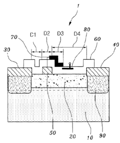
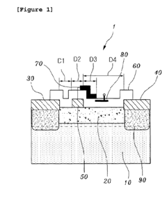
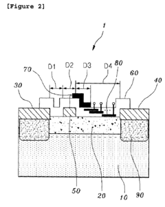
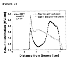
Gallium nitride high electron mobility transistor having inner field-plate for high power applications
PatentInactiveUS7696535B2
Innovation
- Incorporating an inner field-plate between the gate and drain electrodes to distribute the electric field, reduce peak values, and apply varying voltages to the inner field-plate, thereby reducing gate leakage current and capacitance while maintaining high frequency performance.
Gallium nitride material transistors and methods for wideband applications
PatentInactiveUS20070202360A1
Innovation
- The development of gallium nitride material transistors with active regions formed in gallium nitride layers, integrated with matching circuits to achieve low relative constellation error (RCE) values and high efficiency, enabling efficient signal amplification and transmission with excellent linearity and compliance with spectrum mask requirements.
Thermal Management Challenges in GaN Devices
Gallium Nitride (GaN) transistors, while offering superior performance in high-power applications, face significant thermal management challenges that must be addressed for reliable operation. The wide bandgap properties that enable GaN's exceptional electrical performance also create unique thermal considerations. GaN devices typically operate at higher power densities and frequencies than silicon counterparts, generating substantial heat in smaller areas.
The thermal conductivity of GaN (approximately 130 W/m·K) is higher than silicon but becomes a limiting factor when devices operate at extreme power densities. This challenge is compounded by the "self-heating effect," where localized hotspots form within the device structure, particularly at the gate-drain region during high-voltage operation. These hotspots can reach temperatures exceeding 200°C, significantly affecting device reliability and performance.
Interface thermal resistance presents another critical challenge. Most commercial GaN transistors utilize heterogeneous material stacks (GaN-on-Si, GaN-on-SiC, or GaN-on-diamond), creating thermal boundary resistances at material interfaces. These boundaries impede efficient heat dissipation, with the GaN/substrate interface often becoming the primary bottleneck in the thermal pathway.
Package-level thermal management further complicates GaN implementation. Traditional packaging solutions designed for silicon devices often prove inadequate for GaN's thermal requirements. The thermal resistance from junction to case (RθJC) becomes a critical parameter, with advanced packages striving to minimize this value through improved die-attach materials and techniques.
Current thermal management approaches include advanced substrate materials like silicon carbide (SiC) and diamond, which offer thermal conductivities of 370 W/m·K and 2000 W/m·K respectively. However, these solutions introduce manufacturing complexity and increased costs. Novel cooling techniques such as microfluidic cooling channels, phase-change materials, and graphene-based thermal interfaces are being explored to address these challenges.
Simulation and modeling tools have become essential for predicting thermal behavior in GaN devices. Finite element analysis (FEA) and computational fluid dynamics (CFD) enable designers to identify potential hotspots and optimize thermal pathways before physical prototyping. These tools have revealed that transient thermal effects are particularly significant in GaN devices operating in pulsed-power applications, where temperature fluctuations can induce mechanical stress and accelerate device degradation.
The industry continues to develop innovative solutions, including integrated temperature sensors for real-time monitoring and adaptive thermal management systems that adjust operating parameters based on thermal conditions. These advances are crucial for enabling GaN technology to reach its full potential in revolutionizing high-power applications.
GaN Manufacturing Process Optimization
The optimization of Gallium Nitride (GaN) manufacturing processes represents a critical frontier in advancing high-power electronic applications. Current GaN production faces significant challenges including high defect densities, substrate limitations, and cost inefficiencies that impede widespread commercial adoption. Industry leaders have implemented several innovative approaches to overcome these barriers, focusing primarily on epitaxial growth techniques and substrate engineering.
Metal-Organic Chemical Vapor Deposition (MOCVD) remains the dominant method for GaN epitaxial growth, with recent advancements in precursor chemistry and reactor design yielding substantial improvements in film quality. The introduction of pulsed growth sequences has demonstrated remarkable success in reducing threading dislocation densities from 10^9 cm^-2 to below 10^6 cm^-2, significantly enhancing device performance and reliability.
Substrate selection continues to evolve as a critical optimization parameter. While silicon carbide (SiC) substrates offer superior thermal conductivity advantageous for high-power applications, silicon substrates provide cost benefits and integration compatibility with existing semiconductor infrastructure. Recent developments in engineered buffer layers have mitigated the lattice mismatch issues between GaN and silicon, enabling larger wafer diameters (up to 200mm) while maintaining acceptable defect levels.
Surface passivation techniques have undergone substantial refinement, with atomic layer deposition (ALD) of dielectric materials emerging as a preferred method. These ultra-thin conformal layers effectively mitigate surface-related current collapse phenomena that previously limited high-frequency performance. Manufacturers have reported up to 40% improvement in dynamic Ron characteristics through optimized passivation processes.
Vertical device architectures represent another promising manufacturing optimization pathway. Unlike lateral devices, vertical GaN structures can handle higher breakdown voltages and current densities. The manufacturing challenge lies in developing reliable and repeatable processes for creating these complex 3D structures, particularly regarding controlled doping profiles and ohmic contact formation.
Advanced characterization methodologies have become integral to process optimization, with in-situ monitoring techniques providing real-time feedback during growth. Manufacturers employing these systems report up to 30% improvement in wafer-to-wafer consistency and significantly reduced qualification times. Additionally, machine learning algorithms are increasingly being deployed to analyze complex process parameter interactions, identifying optimal manufacturing conditions that human engineers might overlook.
Unlock deeper insights with Patsnap Eureka Quick Research — get a full tech report to explore trends and direct your research. Try now!
Generate Your Research Report Instantly with AI Agent
Supercharge your innovation with Patsnap Eureka AI Agent Platform!