

Gallium Nitride Transistors: Evaluating High-Power Application Risks
OCT 14, 20259 MIN READ
Generate Your Research Report Instantly with AI Agent
PatSnap Eureka helps you evaluate technical feasibility & market potential.
GaN Transistor Evolution and Performance Targets
Gallium Nitride (GaN) transistor technology has evolved significantly since its inception in the early 1990s, transforming from a laboratory curiosity to a commercially viable solution for high-power applications. The initial development phase focused primarily on overcoming material growth challenges, with researchers at major institutions like Bell Labs and the University of California pioneering techniques for creating high-quality GaN crystals on various substrates. This fundamental work established the foundation for subsequent device engineering.
By the early 2000s, the technology progressed to addressing critical performance limitations, particularly the "current collapse" phenomenon that initially restricted GaN's practical utility. The introduction of field plates and advanced passivation techniques marked a significant breakthrough, enabling devices to operate reliably at higher voltages. This period also saw the first commercial GaN transistors entering specialized markets, albeit with limited performance compared to today's standards.
The 2010s witnessed rapid advancement in GaN transistor capabilities, with breakdown voltages increasing from approximately 600V to over 1200V, and current densities improving from 0.5 A/mm to exceeding 2 A/mm in commercial devices. Concurrently, switching frequencies advanced from the sub-MHz range to multi-MHz operation, dramatically reducing system-level power losses in converter applications.
Current technical objectives for GaN transistors center on several key performance targets. First, increasing the breakdown voltage beyond 1500V while maintaining high current capability would enable GaN to penetrate additional high-power market segments currently dominated by silicon carbide. Second, improving thermal management to handle power densities exceeding 5 W/mm² represents a critical goal for applications in electric vehicles and industrial power systems.
Reliability enhancement constitutes another primary objective, with industry targets focusing on achieving failure rates below 10 FIT (failures in time) and operational lifetimes exceeding 15 years under typical application conditions. This requires addressing specific failure mechanisms including time-dependent dielectric breakdown and hot electron degradation that become increasingly problematic at higher operating voltages.
Manufacturing scalability presents an additional technical target, with efforts directed toward 8-inch wafer processing compatibility and cost reduction to below $0.10 per amp-volt figure of merit. The industry is simultaneously pursuing integration capabilities, aiming to incorporate gate drivers, protection circuitry, and sensing functions alongside GaN power devices to create more compact and efficient power solutions.
These evolutionary trends and performance targets reflect GaN transistor technology's trajectory toward becoming the dominant solution for medium-voltage (600-1200V) power applications where efficiency, power density, and switching performance are paramount considerations.
Market Analysis for High-Power GaN Applications
The global market for Gallium Nitride (GaN) transistors in high-power applications is experiencing robust growth, driven by increasing demand for efficient power conversion systems across multiple industries. Current market valuations indicate the GaN power device market reached approximately 223 million USD in 2022, with projections suggesting a compound annual growth rate (CAGR) of 18.1% through 2028, potentially reaching 607 million USD by the end of the forecast period.
Key market segments demonstrating significant adoption include power supplies, data centers, electric vehicles, renewable energy systems, and military/aerospace applications. The electric vehicle sector represents one of the fastest-growing segments, with GaN transistors increasingly being incorporated into onboard chargers and DC-DC converters due to their superior efficiency and reduced form factor compared to silicon alternatives.
Regional analysis reveals that Asia-Pacific currently dominates the GaN high-power market, accounting for approximately 45% of global demand. This is primarily attributed to the strong presence of semiconductor manufacturing facilities and the rapid expansion of electric vehicle production in countries like China, Japan, and South Korea. North America follows with roughly 30% market share, driven by defense applications and data center infrastructure development.
Customer demand patterns indicate a growing preference for higher voltage ratings, with 650V GaN transistors currently representing the largest market segment. However, the 900-1200V segment is experiencing the fastest growth rate as applications in industrial power supplies and renewable energy systems expand. This shift is creating new market opportunities for manufacturers capable of addressing reliability concerns at these higher voltage ratings.
Market barriers include the relatively higher cost of GaN devices compared to silicon alternatives, concerns about long-term reliability in mission-critical applications, and the need for specialized design expertise. Despite these challenges, the price premium for GaN solutions continues to decrease as manufacturing volumes increase and yield rates improve.
Competitive dynamics show an evolving landscape with both established power semiconductor companies and specialized GaN startups vying for market share. Strategic partnerships between GaN device manufacturers and end-system designers are becoming increasingly common, particularly in automotive applications where qualification requirements are stringent and design cycles are lengthy.
Market forecasts suggest that as reliability concerns are addressed through improved packaging technologies and accumulated field data, adoption rates will accelerate significantly in the 2025-2028 timeframe, particularly in high-voltage applications above 900V where silicon carbide (SiC) currently maintains advantages in certain performance metrics.
Current GaN Technology Limitations and Challenges
Despite significant advancements in Gallium Nitride (GaN) transistor technology, several critical limitations and challenges persist that impact their widespread adoption in high-power applications. The primary technical constraint remains the current collapse phenomenon, where device performance degrades under high-voltage switching conditions due to electron trapping effects at the surface and buffer layers. This results in increased dynamic on-resistance and reduced reliability during operation.
Thermal management presents another significant challenge for GaN transistors. While theoretically capable of operating at higher temperatures than silicon, practical implementations face difficulties in heat dissipation due to packaging limitations and thermal boundary resistance issues. The thermal conductivity of GaN substrates, particularly those grown on silicon, remains inferior to silicon carbide alternatives, creating hotspots that can lead to premature device failure.
Manufacturing yield and consistency issues continue to plague GaN technology. The epitaxial growth process on foreign substrates (typically silicon) introduces crystal defects and dislocations that compromise device performance and reliability. These defects serve as electron trapping centers and leakage current pathways, contributing to device degradation over time. The industry has yet to establish standardized qualification procedures specifically tailored for GaN reliability assessment.
Cost factors remain prohibitive for many applications. While GaN-on-Silicon has reduced costs compared to native substrates, the overall manufacturing expenses still exceed those of conventional silicon technologies. The specialized equipment required for GaN processing and the additional manufacturing steps contribute to higher production costs that limit market penetration beyond premium applications.
Integration challenges persist when incorporating GaN devices into existing systems. The faster switching speeds of GaN transistors, while beneficial for efficiency, create electromagnetic interference (EMI) issues that require careful circuit design and layout considerations. Additionally, gate driving requirements differ significantly from silicon MOSFETs, necessitating specialized driver circuits that add complexity and cost.
Reliability concerns continue to hinder adoption in mission-critical applications. Long-term stability under high-field conditions remains inadequately characterized, with limited industry data on failure mechanisms and lifetime predictions. The time-dependent breakdown of gate dielectrics and buffer layers represents a particular concern for applications requiring decades of reliable operation.
Standardization gaps further complicate the landscape. Unlike mature silicon technologies, GaN transistors lack comprehensive industry standards for characterization, qualification, and application guidelines. This absence creates uncertainty for system designers and slows adoption in conservative industries such as automotive and industrial power electronics.
Existing GaN High-Power Implementation Strategies
01 Thermal management risks in GaN transistors
Gallium Nitride transistors face significant thermal management challenges due to their high power density operation. These devices can generate substantial heat during operation, which if not properly dissipated, can lead to performance degradation, reduced reliability, and potential device failure. Thermal runaway is a particular concern where increasing temperature leads to higher leakage currents, creating a dangerous feedback loop. Advanced cooling solutions and thermal design considerations are essential to mitigate these risks.- Thermal management risks in GaN transistors: Gallium Nitride transistors face significant thermal management challenges due to their high power density operation. The heat generated during operation can lead to device degradation, reduced reliability, and potential failure if not properly dissipated. These thermal risks are particularly pronounced in high-frequency and high-power applications where GaN transistors operate at their performance limits, requiring advanced cooling solutions and thermal design considerations.
- Manufacturing defects and crystal structure risks: The manufacturing process of GaN transistors presents risks related to crystal defects, dislocations, and impurities in the semiconductor material. These structural imperfections can compromise device performance, reduce yield rates, and create reliability issues. The challenges in growing high-quality GaN crystals and maintaining structural integrity during fabrication processes can lead to inconsistent device characteristics and premature failure mechanisms in the transistors.
- Electrical breakdown and reliability concerns: GaN transistors face risks related to electrical breakdown under high voltage and current conditions. Despite their theoretical advantages in breakdown voltage, practical implementations can suffer from premature breakdown due to electric field crowding at edges, surface states, and buffer layer issues. Long-term reliability concerns include threshold voltage shifts, current collapse phenomena, and degradation mechanisms that emerge during extended operation, particularly under switching stress conditions.
- Interface and passivation challenges: The interface between GaN and other materials in transistor structures presents significant risks. Poor interface quality can lead to electron trapping, current collapse, and degraded device performance. Additionally, inadequate surface passivation can result in increased leakage currents, reduced breakdown voltage, and reliability issues. These interface challenges affect both the gate region and the overall device structure, impacting the stability and performance of GaN transistors in various applications.
- Integration and compatibility issues: GaN transistors face integration challenges when incorporated into existing semiconductor technology platforms. Compatibility issues arise from differences in processing requirements, thermal expansion coefficients, and electrical characteristics compared to silicon-based devices. These integration risks can lead to increased manufacturing complexity, higher costs, and potential reliability concerns in hybrid circuits. Additionally, specialized packaging solutions are often required to address the unique thermal and electrical characteristics of GaN transistors.
02 Reliability and degradation mechanisms
GaN transistors are susceptible to various degradation mechanisms that affect long-term reliability. These include current collapse phenomena, gate leakage, and electron trapping effects that can occur at high voltage operation. Material defects in the GaN crystal structure can propagate during operation, leading to premature device failure. Environmental factors such as humidity and temperature cycling can accelerate these degradation processes, making reliability testing and qualification particularly important for mission-critical applications.Expand Specific Solutions03 Manufacturing defects and quality control issues
The fabrication of GaN transistors presents unique challenges that can lead to manufacturing defects. Issues such as crystal dislocations, impurities, and non-uniform epitaxial growth can compromise device performance and reliability. The interface between GaN and substrate materials often contains defects that can propagate during operation. Quality control processes must be stringent to identify these defects before devices reach end applications, as latent defects may not manifest until after extended operation in the field.Expand Specific Solutions04 Electrical overstress and breakdown risks
GaN transistors are vulnerable to electrical overstress conditions that can cause catastrophic failure. Despite their high breakdown voltage capabilities, these devices can experience gate oxide breakdown, buffer breakdown, or channel burnout when operated beyond specified limits. Transient voltage spikes, common in power switching applications, pose particular risks to GaN devices. Protection circuits and robust design margins are necessary to prevent damage from electrical overstress events that could otherwise lead to immediate failure or accelerated aging.Expand Specific Solutions05 Integration and compatibility challenges
Integrating GaN transistors into existing systems presents compatibility challenges that can increase implementation risks. The unique driving requirements, faster switching speeds, and electromagnetic interference characteristics of GaN devices require careful system design. Parasitic inductances in circuit layouts can cause voltage overshoots and ringing that damage devices. Additionally, GaN transistors may have different failure modes compared to silicon devices, necessitating new protection schemes and design approaches to ensure safe and reliable operation in electronic systems.Expand Specific Solutions
Leading GaN Semiconductor Manufacturers and Competitors
Gallium Nitride (GaN) transistors are currently in a growth phase within the high-power applications market, with an estimated market size exceeding $1.5 billion and projected to grow at 20% CAGR through 2027. The technology has reached moderate maturity, with key players demonstrating different levels of advancement. Industry leaders like Wolfspeed, GaN Systems, and Innoscience have established commercial product lines, while semiconductor giants including NXP, Texas Instruments, and Infineon are expanding their GaN portfolios. Research institutions such as UESTC and HKUST continue to address technical challenges. The competitive landscape shows a mix of specialized GaN-focused companies and diversified semiconductor manufacturers, with recent innovations focusing on improving reliability, thermal management, and cost reduction for high-power applications.
Wolfspeed, Inc.
Technical Solution: Wolfspeed has pioneered silicon carbide and gallium nitride (GaN) solutions for high-power applications, with their GaN HEMT (High Electron Mobility Transistor) technology offering superior performance in power density and efficiency. Their GaN-on-SiC platform delivers transistors capable of operating at frequencies exceeding 100 GHz with power densities of 5-7 W/mm[1]. Wolfspeed's approach focuses on vertical GaN power devices that can handle breakdown voltages above 1200V while maintaining low on-resistance. Their proprietary epitaxial growth techniques create high-quality GaN layers with controlled doping profiles, reducing defect densities that could otherwise lead to premature device failure under high-power conditions[2]. The company has developed specialized passivation techniques to mitigate surface-related breakdown mechanisms, enhancing reliability in high-field environments typical in power applications.
Strengths: Industry-leading power density and frequency performance; superior thermal management through SiC substrates; established manufacturing infrastructure for volume production. Weaknesses: Higher cost compared to silicon alternatives; requires specialized packaging solutions to fully utilize thermal capabilities; reliability concerns remain for extreme operating conditions beyond standard qualification tests.
Texas Instruments Incorporated
Technical Solution: Texas Instruments has developed an integrated GaN solution focusing on system-level optimization rather than discrete transistors alone. Their GaN technology incorporates driver integration with power stage components, addressing one of the key challenges in high-power GaN applications - the critical interaction between driver and transistor[1]. TI's approach includes specialized gate drive techniques that precisely control switching transitions, minimizing voltage overshoots that could lead to reliability issues. Their GaN platform features comprehensive protection mechanisms including overcurrent, overvoltage, and overtemperature protection circuits specifically calibrated for GaN's unique characteristics and failure modes. For high-power applications, TI has developed advanced thermal management solutions including innovative package designs and die-attach materials that maximize heat dissipation while maintaining electrical performance. Their reliability testing methodology includes mission-profile based qualification that simulates actual application conditions rather than just standard qualification tests, providing more realistic assessment of long-term reliability in high-power applications[2].
Strengths: System-level approach integrating driver and protection features; extensive application knowledge across multiple power conversion topologies; strong manufacturing quality systems. Weaknesses: More focused on medium-power applications than extreme high-power applications; relatively conservative voltage ratings compared to some competitors; integration approach may limit flexibility for some specialized applications.
Critical GaN Reliability and Failure Mode Analysis
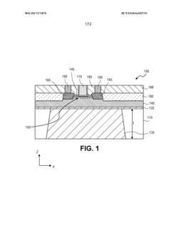
Gallium nitride transistor with underfill aluminum nitride for improved thermal and RF performance
PatentWO2017171870A1
Innovation
- Incorporating an aluminum nitride layer under the gallium nitride transistor or circuit block, utilizing a low resistivity silicon substrate, which provides both high thermal conductivity and high resistivity through the aluminum nitride's insulating properties and superior thermal conductivity compared to silicon.
High Temperature Performance Capable Gallium Nitride Transistor
PatentActiveEP2385558A2
Innovation
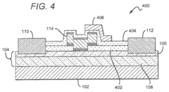
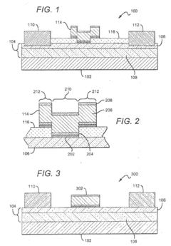
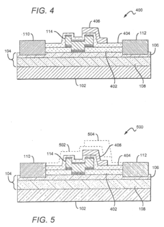
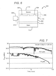
- The transistors incorporate a gate electrode made from materials with high Schottky barriers, such as nickel-chromium alloys or polycrystalline indium nitride, and a spacer layer structure with a field plate to reduce peak electric fields and enhance durability at high temperatures, including a diffusion barrier and protective layers to prevent inter-diffusion and damage.
Thermal Management Solutions for GaN Devices
Thermal management represents a critical challenge in the deployment of Gallium Nitride (GaN) transistors for high-power applications. As GaN devices operate at significantly higher power densities than traditional silicon-based semiconductors, they generate substantial heat that must be efficiently dissipated to maintain performance and reliability.
Conventional cooling techniques such as forced-air convection and passive heat sinks have proven inadequate for managing the thermal loads generated by GaN transistors in high-power scenarios. Advanced thermal management solutions have emerged to address these challenges, including direct liquid cooling systems that offer thermal conductivity values 10-100 times higher than air-based solutions.
Microfluidic cooling channels integrated directly into GaN device packaging represent a promising approach, allowing coolant to flow in close proximity to heat-generating regions. These systems have demonstrated the ability to maintain junction temperatures below 150°C even at power densities exceeding 1000 W/cm². Diamond-based heat spreaders, with thermal conductivity values up to 2000 W/mK, offer another effective solution for managing localized hotspots in GaN devices.
Phase-change materials (PCMs) incorporated into GaN packaging provide thermal buffering during transient operation, absorbing heat during power spikes and releasing it during low-power periods. This approach has shown particular value in pulsed-power applications where thermal cycling presents reliability concerns.
Advanced thermal interface materials (TIMs) with enhanced thermal conductivity and reduced thermal boundary resistance are being developed specifically for GaN applications. Graphene-enhanced TIMs have demonstrated up to 45% improvement in thermal performance compared to conventional materials when implemented with GaN devices.
Computational fluid dynamics (CFD) modeling has become essential for optimizing thermal management solutions for GaN transistors. These simulation tools enable precise prediction of temperature distributions and hotspots, allowing designers to evaluate cooling strategies before physical implementation. Recent advances in multi-physics modeling permit simultaneous analysis of electrical, thermal, and mechanical behaviors in GaN devices.
Industry standards for thermal characterization of GaN devices are still evolving, with organizations like JEDEC developing specialized test methods for wide-bandgap semiconductors. These standards will be crucial for consistent evaluation of thermal management solutions across different GaN technologies and applications, ultimately reducing implementation risks in high-power systems.
Safety Standards and Certification Requirements
The implementation of Gallium Nitride (GaN) transistors in high-power applications necessitates adherence to rigorous safety standards and certification requirements. Currently, the regulatory framework for GaN technology spans multiple jurisdictions with varying degrees of specificity. In the United States, the UL 1557 standard for "Electrically Isolated Semiconductor Devices" provides baseline requirements, though it was not specifically developed for wide-bandgap semiconductors like GaN. The IEC 60747 series, particularly IEC 60747-8 for "Semiconductor devices - Discrete devices," offers international guidelines that manufacturers must consider.
For automotive applications, the AEC-Q101 qualification is essential, requiring GaN transistors to demonstrate reliability under extreme temperature cycling, humidity, and electrical stress conditions. However, industry experts note that these standards were primarily developed for silicon-based technologies and may not fully address the unique characteristics of GaN devices, particularly their faster switching speeds and higher operating temperatures.
The European Union's requirements under the Low Voltage Directive (2014/35/EU) and Electromagnetic Compatibility Directive (2014/30/EU) impose additional compliance burdens for GaN transistors entering European markets. Manufacturers must obtain CE marking, demonstrating conformity with health, safety, and environmental protection standards. This process typically involves third-party testing and documentation of safety measures.
In high-reliability applications such as aerospace and defense, MIL-STD-750 testing methods for semiconductor devices apply, with specific attention to radiation hardness and extended reliability testing. These certifications can take 12-18 months to complete, representing a significant barrier to market entry for new GaN solutions.
The thermal management capabilities of GaN devices must be certified according to JEDEC standards, particularly JESD22-A105C for power and temperature cycling. Recent research indicates that traditional thermal testing protocols may underestimate junction temperatures in GaN HEMTs by up to 15%, potentially compromising long-term reliability assessments.
Emerging standards specifically addressing GaN technology include the JEDEC JC-70.1 committee's work on standardizing dynamic on-resistance measurements and threshold voltage stability. Industry consortia like the GaN Standards Initiative are also developing application-specific guidelines for power conversion, RF amplification, and automotive systems.
Certification costs represent a significant consideration, with comprehensive safety certification packages potentially exceeding $100,000 per device family. This financial burden disproportionately affects smaller manufacturers and startups, potentially limiting innovation in the GaN ecosystem. The certification timeline, averaging 6-9 months for commercial applications and longer for specialized sectors, also impacts time-to-market strategies.
Unlock deeper insights with PatSnap Eureka Quick Research — get a full tech report to explore trends and direct your research. Try now!
Generate Your Research Report Instantly with AI Agent
Supercharge your innovation with PatSnap Eureka AI Agent Platform!