Gallium Nitride Transistors and their Role in Modern Aerospace Functionality
OCT 14, 202510 MIN READ
Generate Your Research Report Instantly with AI Agent
Patsnap Eureka helps you evaluate technical feasibility & market potential.
GaN Transistor Evolution and Aerospace Goals
Gallium Nitride (GaN) technology has undergone significant evolution since its initial development in the early 1990s. The journey began with fundamental research into wide bandgap semiconductors, where GaN's exceptional properties—including high breakdown voltage, high electron mobility, and excellent thermal conductivity—were first recognized. These characteristics positioned GaN as a superior alternative to traditional silicon-based semiconductors for high-power, high-frequency applications.
The evolution of GaN transistors can be traced through several distinct phases. The first generation, developed in the late 1990s, focused primarily on proving the concept and addressing basic fabrication challenges. These early devices demonstrated promising performance but suffered from reliability issues and high production costs. The second generation, emerging in the early 2000s, saw significant improvements in manufacturing processes, leading to enhanced device stability and reduced defect densities.
By the 2010s, third-generation GaN transistors achieved commercial viability, with substantial improvements in power handling capabilities, switching speeds, and thermal management. Current fourth-generation devices incorporate advanced packaging technologies, innovative substrate materials, and sophisticated gate structures that further optimize performance while reducing size and weight—critical factors for aerospace applications.
In the aerospace sector, GaN transistor technology aims to address several critical goals. Primary among these is the enhancement of radar and communication systems' performance. GaN-based power amplifiers enable higher transmission power, increased bandwidth, and improved signal quality, resulting in extended range and resolution for radar systems and higher data rates for communication networks.
Another key objective is the reduction of size, weight, and power consumption (SWaP) in aerospace electronic systems. GaN transistors operate at higher voltages and frequencies than silicon alternatives, allowing for more compact and efficient designs. This translates directly to fuel savings, increased payload capacity, and extended mission durations for aircraft and spacecraft.
Reliability under extreme conditions represents another crucial goal. Aerospace applications demand components that can withstand wide temperature variations, radiation exposure, and mechanical stress. GaN's inherent material properties make it exceptionally suitable for these harsh environments, with ongoing research focused on further enhancing reliability through improved passivation techniques and packaging solutions.
Looking forward, the aerospace industry is driving GaN technology toward even higher levels of integration and functionality. The development of GaN-based monolithic microwave integrated circuits (MMICs) promises to revolutionize aerospace electronics by combining multiple functions on single chips, further reducing size and weight while improving system performance and reliability.
Aerospace Market Demand for GaN Technology
The aerospace industry has witnessed a significant shift towards advanced semiconductor technologies, with Gallium Nitride (GaN) transistors emerging as a critical component for next-generation aerospace systems. Market analysis indicates that the global aerospace GaN market is projected to grow at a compound annual growth rate of 22% through 2028, driven primarily by increasing demands for high-performance radar systems, satellite communications, and electronic warfare capabilities.
Defense applications represent the largest segment of aerospace GaN demand, accounting for approximately 65% of the market. Military aircraft modernization programs across major defense powers including the United States, China, and European nations are actively incorporating GaN-based radar and communication systems to achieve superior range, resolution, and electronic countermeasure capabilities. The AESA (Active Electronically Scanned Array) radar market alone is expected to reach $17 billion by 2026, with GaN technology becoming the preferred solution for transmit/receive modules.
Commercial aerospace applications are also driving significant demand for GaN technology. Satellite communications systems benefit tremendously from GaN's efficiency at high frequencies, enabling higher data throughput with reduced power consumption. The rapidly expanding low Earth orbit (LEO) satellite constellations for global internet coverage have created a surge in demand for GaN-based power amplifiers and RF components. Companies like SpaceX, OneWeb, and Amazon's Project Kuiper collectively plan to deploy over 20,000 satellites, creating sustained demand for GaN technology.
The unique operating environment of aerospace applications perfectly aligns with GaN's inherent advantages. The extreme temperature conditions encountered in aerospace (-65°C to +150°C) require semiconductor technologies with exceptional thermal stability. GaN's wide bandgap properties enable reliable operation across this temperature range, reducing the need for complex thermal management systems and improving overall system reliability.
Radiation hardness represents another critical market driver for aerospace GaN adoption. Satellite systems operating in space are exposed to significant radiation that can degrade conventional semiconductor performance. GaN's inherent radiation tolerance makes it particularly valuable for space applications, with market research indicating that radiation-hardened GaN components command premium pricing, often 3-5 times higher than commercial equivalents.
The push toward more electric aircraft (MEA) and unmanned aerial vehicles (UAVs) is creating additional demand vectors for GaN technology. Power conversion systems benefit from GaN's high-efficiency operation, enabling lighter and more compact designs that directly translate to fuel savings and extended mission capabilities. The UAV market segment is experiencing particularly rapid growth, with military, commercial, and research applications all contributing to increased GaN demand.
GaN Transistor Development Status and Challenges
Gallium Nitride (GaN) transistors have emerged as a revolutionary technology in the aerospace industry, offering significant advantages over traditional silicon-based semiconductors. Currently, GaN transistors are at a mature development stage for radio frequency (RF) applications, with commercial products available from multiple manufacturers. However, power electronics applications are still evolving rapidly, with ongoing improvements in device reliability and performance.
The global landscape of GaN technology development shows distinct regional strengths. The United States leads in military and aerospace applications, with substantial government funding supporting research at institutions like MIT, University of California, and major defense contractors. Europe has established strong research clusters in Germany and France, focusing on automotive and industrial applications. Meanwhile, Japan and South Korea have made significant advancements in consumer electronics applications of GaN technology.
Despite impressive progress, several critical challenges remain in GaN transistor development. Thermal management represents a primary concern, as GaN devices generate substantial heat during high-power operation. Current cooling solutions are often inadequate for aerospace applications where size and weight constraints are paramount. Researchers are exploring advanced thermal interface materials and novel packaging techniques to address this limitation.
Reliability under extreme conditions poses another significant challenge. Aerospace environments subject components to radiation, temperature cycling, and mechanical stress that can accelerate device degradation. Current qualification standards for GaN devices in aerospace applications remain inconsistent across the industry, complicating implementation decisions.
Manufacturing scalability continues to limit widespread adoption. While 6-inch GaN wafer production is standard, the transition to 8-inch wafers has been slower than anticipated, keeping costs relatively high compared to silicon alternatives. Defect densities in GaN epitaxial layers remain higher than ideal, affecting yield and reliability.
Integration challenges persist when incorporating GaN devices into existing aerospace systems. The different driving requirements and switching characteristics of GaN transistors often necessitate redesigning entire power management architectures to fully leverage their benefits. This creates a significant barrier to adoption in legacy aerospace platforms.
Cost factors remain a constraint, particularly for commercial aerospace applications where economic considerations are paramount. Though prices have decreased substantially over the past decade, GaN transistors still command a premium over silicon alternatives, requiring clear performance advantages to justify implementation.
Research efforts are intensifying to overcome these limitations, with particular focus on novel buffer layer designs to reduce defects, advanced packaging solutions for improved thermal performance, and radiation-hardened variants specifically engineered for space applications.
Current GaN Implementation in Aerospace Systems
01 Fabrication methods for GaN transistors
Various methods for manufacturing gallium nitride transistors have been developed to improve device performance. These methods include specialized growth techniques for GaN layers, substrate preparation processes, and post-growth treatments. The fabrication processes often focus on reducing defects and improving crystal quality, which directly impacts the electrical properties of the resulting transistors. Advanced epitaxial growth techniques and precise control of growth parameters are essential for high-quality GaN transistor fabrication.- Fabrication methods for GaN transistors: Various methods for fabricating gallium nitride transistors have been developed to improve performance and reliability. These methods include specialized deposition techniques, substrate preparation, and layer structuring to enhance electron mobility and reduce defects. Advanced fabrication processes enable the creation of high-quality GaN transistor structures with improved electrical characteristics and thermal stability.
- GaN transistor structural designs: Innovative structural designs for gallium nitride transistors focus on optimizing device architecture for enhanced performance. These designs include various gate configurations, channel structures, and buffer layer arrangements to improve electron transport and reduce parasitic effects. Structural innovations help address challenges related to current collapse, breakdown voltage, and on-resistance in high-power applications.
- GaN substrate and crystal growth technologies: Technologies for growing high-quality gallium nitride crystals and substrates are crucial for transistor performance. These include methods for reducing dislocation density, controlling crystal orientation, and achieving uniform material properties. Advanced substrate technologies enable the production of GaN transistors with improved carrier mobility, breakdown voltage, and thermal conductivity.
- GaN-based heterostructure transistors: Heterostructure designs incorporating gallium nitride with other materials create advanced transistor capabilities. These structures typically include combinations of GaN with AlGaN, InGaN, or other III-nitride materials to form two-dimensional electron gas regions with high carrier mobility. Such heterostructure designs enable high-frequency operation, improved power handling, and enhanced efficiency in power electronics applications.
- GaN transistor packaging and thermal management: Specialized packaging and thermal management solutions address the unique challenges of gallium nitride transistors operating at high power densities. These include advanced heat dissipation structures, novel die-attach materials, and optimized package designs to maintain device reliability. Effective thermal management is critical for maximizing the performance and operational lifetime of GaN transistors in high-power applications.
02 GaN transistor device structures
Innovative device structures have been designed to enhance the performance of gallium nitride transistors. These structures include various configurations of high electron mobility transistors (HEMTs), heterojunction field-effect transistors (HFETs), and metal-oxide-semiconductor field-effect transistors (MOSFETs). The designs often incorporate specialized layers, such as buffer layers, barrier layers, and channel layers, to optimize electron transport and reduce parasitic effects. Novel gate structures and contact designs are also implemented to improve device characteristics.Expand Specific Solutions03 GaN substrate and crystal growth technology
The quality of gallium nitride substrates significantly impacts transistor performance. Advanced crystal growth technologies have been developed to produce high-quality GaN substrates with reduced defect densities. These technologies include hydride vapor phase epitaxy (HVPE), metal-organic chemical vapor deposition (MOCVD), and molecular beam epitaxy (MBE). Techniques for growing GaN on various substrates such as sapphire, silicon carbide, and silicon have been optimized to address lattice mismatch issues and improve crystal quality.Expand Specific Solutions04 Power electronics applications of GaN transistors
Gallium nitride transistors offer significant advantages for power electronics applications due to their high breakdown voltage, high electron mobility, and excellent thermal conductivity. These transistors are used in high-frequency power converters, inverters, and power supplies, enabling higher efficiency and power density compared to conventional silicon-based devices. GaN transistors also demonstrate superior performance in high-temperature environments, making them suitable for automotive and industrial applications where reliability under harsh conditions is critical.Expand Specific Solutions05 Enhancement techniques for GaN transistor performance
Various techniques have been developed to enhance the performance of gallium nitride transistors. These include surface passivation methods to reduce current collapse and improve reliability, field plate structures to increase breakdown voltage, and advanced doping profiles to optimize carrier concentration. Other enhancement approaches involve novel gate dielectrics, improved ohmic contacts, and specialized heat dissipation structures. These techniques collectively contribute to improving key transistor parameters such as on-resistance, switching speed, and overall efficiency.Expand Specific Solutions
Leading GaN Transistor Manufacturers and Aerospace Partners
Gallium Nitride (GaN) transistors are revolutionizing aerospace functionality, currently positioned at the early growth stage of industry development. The market is expanding rapidly, projected to reach significant scale as aerospace applications increasingly demand high-frequency, high-power, and high-temperature capabilities. Technologically, GaN transistors are transitioning from emerging to mature status, with key players demonstrating varying levels of advancement. Companies like Wolfspeed, GaN Systems, and Raytheon lead with established GaN expertise, while Intel, NXP, and Infineon leverage their semiconductor infrastructure to accelerate development. Emerging players including Cambridge GaN Devices and Navitas Semiconductor are introducing innovative approaches. Chinese entities such as Huawei and Innoscience are rapidly closing the technology gap, while research institutions like Xidian University and the National Research Council of Canada continue pushing fundamental boundaries in GaN aerospace applications.
MACOM Technology Solutions Holdings, Inc.
Technical Solution: MACOM has pioneered GaN-on-Silicon technology specifically optimized for aerospace applications, offering significant cost advantages over traditional GaN-on-SiC approaches. Their aerospace GaN portfolio includes high-power RF amplifiers operating at frequencies up to 18GHz with power levels exceeding 100W per device. MACOM's proprietary GaN fabrication process achieves device lifetimes exceeding 1 million hours at 200°C channel temperatures, meeting the stringent reliability requirements of aerospace systems. Their GaN solutions feature integrated protection circuitry that enables robust operation in the harsh electromagnetic environments encountered in aerospace applications. MACOM has developed specialized packaging technologies that maintain thermal resistances below 2°C/W while meeting the mechanical robustness requirements for high-vibration aerospace environments.
Strengths: Cost-effective GaN-on-Silicon technology; extensive RF design expertise; established supply chain relationships with major aerospace manufacturers. Weaknesses: Lower power density compared to GaN-on-SiC alternatives; frequency performance limitations above Ka-band; thermal management challenges in highest power applications.
GaN Systems, Inc.
Technical Solution: GaN Systems has developed specialized high-reliability GaN transistors targeting aerospace power conversion applications. Their aerospace-grade GaN transistors operate at switching frequencies exceeding 1MHz with efficiencies above 98%, enabling significant size and weight reductions in critical aerospace power systems. The company's patented Island Technology® substrate design enhances thermal performance and reliability by optimizing current dispersion across the device. Their GaN solutions feature integrated gate protection and specialized packaging designed to withstand the extreme temperature cycling (-55°C to +125°C) encountered in aerospace environments. GaN Systems has demonstrated radiation-hardened versions of their transistors maintaining full functionality after exposure to neutron fluences exceeding 10^13 n/cm², addressing a critical requirement for satellite and high-altitude aerospace applications.
Strengths: Industry-leading power efficiency; compact form factors enabling significant system miniaturization; comprehensive design support ecosystem including simulation models and reference designs. Weaknesses: Limited RF/microwave product offerings compared to competitors; relatively newer entrant to aerospace qualification standards; higher unit costs compared to silicon alternatives.
Key GaN Transistor Patents and Technical Innovations
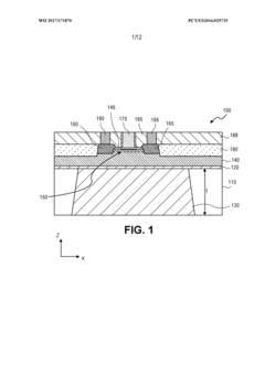
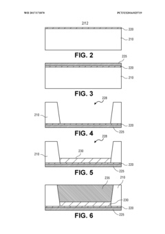
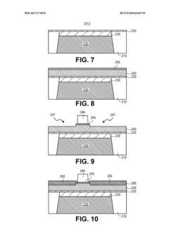
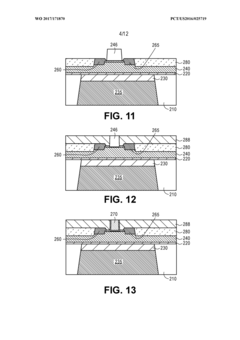
Gallium nitride material transistors and methods associated with the same
PatentInactiveUS7994540B2
Innovation
- The development of gallium nitride material transistors with active regions formed in a gallium nitride layer, integrated with a matching circuit to transform impedance, enabling the amplification of input signals to produce output signals with an adjacent channel power ratio (ACPR) of less than or equal to −20 dBc, while maintaining high drain efficiencies and output powers.
Gallium nitride transistor with underfill aluminum nitride for improved thermal and RF performance
PatentWO2017171870A1
Innovation
- Incorporating an aluminum nitride layer under the gallium nitride transistor or circuit block, utilizing a low resistivity silicon substrate, which provides both high thermal conductivity and high resistivity through the aluminum nitride's insulating properties and superior thermal conductivity compared to silicon.
Reliability and Radiation Hardness of GaN in Space Environments
The space environment presents unique challenges for electronic components due to extreme temperature variations, vacuum conditions, and most critically, high levels of radiation. Gallium Nitride (GaN) transistors have demonstrated remarkable resilience in these harsh conditions, making them increasingly valuable for aerospace applications. Studies indicate that GaN devices exhibit superior radiation hardness compared to traditional silicon-based semiconductors, with total ionizing dose (TID) tolerance often exceeding 1 Mrad, whereas silicon devices typically show degradation at much lower radiation levels.
The inherent properties of GaN contribute significantly to this radiation hardness. The wide bandgap (3.4 eV) and strong atomic bonds in the crystal structure provide natural resistance against displacement damage caused by high-energy particles. Furthermore, the high electron mobility and saturation velocity in GaN devices allow them to maintain functionality even when subjected to radiation-induced carrier removal effects.
Temperature stability represents another critical advantage of GaN in space applications. These transistors can operate reliably across temperature ranges from -55°C to over 300°C, far exceeding the capabilities of silicon alternatives. This thermal robustness eliminates the need for complex cooling systems, reducing overall system weight and complexity in spacecraft designs.
Long-term reliability testing has demonstrated impressive mean time to failure (MTTF) metrics for GaN devices under accelerated life testing conditions. Recent data from NASA and ESA qualification programs show GaN HEMTs maintaining performance parameters within acceptable limits after thousands of hours of operation under simulated space conditions, including thermal cycling and radiation exposure.
The reliability of GaN devices in space is further enhanced by advances in packaging technology. Hermetically sealed packages with improved thermal management capabilities have addressed earlier concerns about package-related failures in vacuum environments. Additionally, specialized passivation techniques have been developed to mitigate surface-related degradation mechanisms that previously limited device longevity.
Despite these advantages, challenges remain in fully qualifying GaN for mission-critical space applications. Single event effects (SEEs), particularly single event gate rupture (SEGR), continue to be areas of concern requiring mitigation strategies. Current research focuses on developing enhanced gate structures and protective circuitry to further improve SEE resilience without compromising the performance benefits of GaN technology.
The radiation hardness assurance (RHA) methodology for GaN devices has evolved significantly, with standardized testing protocols now established by agencies like NASA and ESA. These protocols include comprehensive evaluation of total ionizing dose effects, displacement damage, and single event effects under conditions that accurately simulate the space radiation environment.
Thermal Management Solutions for Aerospace GaN Applications
Thermal management represents a critical challenge in the deployment of Gallium Nitride (GaN) transistors for aerospace applications. The inherent high-power density capabilities of GaN devices, while advantageous for performance, generate significant heat that must be effectively dissipated to maintain reliability and operational longevity in the demanding aerospace environment.
Current thermal management solutions for aerospace GaN applications employ multi-faceted approaches. Advanced packaging techniques utilizing materials with superior thermal conductivity, such as diamond-copper composites and aluminum silicon carbide (AlSiC), have demonstrated considerable effectiveness in heat dissipation. These materials offer thermal conductivity values exceeding 600 W/mK, significantly outperforming traditional aluminum-based solutions.
Active cooling systems have evolved substantially for aerospace GaN implementations. Micro-channel liquid cooling technologies, which circulate coolants through miniaturized channels directly beneath GaN devices, have achieved thermal resistance values below 0.1°C/W. These systems can effectively manage heat loads exceeding 1000 W/cm², making them particularly suitable for high-power radar and electronic warfare applications.
Phase-change materials (PCMs) represent an emerging solution for transient thermal management in aerospace GaN systems. These materials absorb excess heat during peak operation by changing phase, typically from solid to liquid, effectively buffering temperature spikes. Recent aerospace-grade PCMs demonstrate melting points between 40-80°C with latent heat capacities exceeding 200 J/g, providing effective thermal regulation without additional power requirements.
Thermal simulation and modeling tools have become indispensable in aerospace GaN thermal management. Advanced computational fluid dynamics (CFD) models now incorporate multi-physics capabilities that simultaneously analyze electrical, thermal, and mechanical behaviors. These tools enable accurate prediction of hotspot formation and thermal gradients across complex three-dimensional structures, reducing design iterations and accelerating qualification processes.
Integration of thermal management within system-level design represents the frontier of aerospace GaN thermal solutions. Holistic approaches that consider thermal pathways from the semiconductor junction through to the ultimate heat sink have demonstrated temperature reductions of 15-30°C compared to component-level solutions. These integrated designs incorporate thermal vias, embedded heat pipes, and optimized airflow channels to create comprehensive thermal management ecosystems.
The aerospace industry continues to explore novel cooling technologies, including two-phase immersion cooling and graphene-based thermal interface materials, which promise thermal conductivity improvements exceeding 40% over current solutions while meeting stringent reliability requirements for aerospace certification.
Unlock deeper insights with Patsnap Eureka Quick Research — get a full tech report to explore trends and direct your research. Try now!
Generate Your Research Report Instantly with AI Agent
Supercharge your innovation with Patsnap Eureka AI Agent Platform!