Research on the Impact of Material Science in Gallium Nitride Transistors
OCT 14, 202510 MIN READ
Generate Your Research Report Instantly with AI Agent
Patsnap Eureka helps you evaluate technical feasibility & market potential.
GaN Transistor Evolution and Research Objectives
Gallium Nitride (GaN) transistor technology has evolved significantly over the past three decades, transforming from a laboratory curiosity to a commercial reality with substantial impact across multiple industries. The journey began in the early 1990s when researchers first demonstrated the potential of GaN as a semiconductor material for high-power, high-frequency applications. This wide-bandgap semiconductor offered theoretical performance capabilities far exceeding those of traditional silicon-based devices, particularly in terms of breakdown voltage, electron mobility, and thermal conductivity.
The evolution of GaN transistors can be traced through several distinct phases. The initial research phase (1990-2000) focused on fundamental material science challenges, including substrate development, epitaxial growth techniques, and basic device structures. During this period, researchers struggled with high defect densities and limited understanding of GaN's unique properties. The development phase (2000-2010) saw significant improvements in material quality and the emergence of the first commercially viable GaN high-electron-mobility transistors (HEMTs).
From 2010 onwards, we have witnessed the commercialization and refinement phase, with GaN transistors finding applications in RF power amplifiers, power conversion systems, and increasingly in automotive and consumer electronics. This progression has been enabled by continuous advancements in material science, particularly in epitaxial growth techniques, substrate engineering, and interface control.
The current research objectives in GaN transistor technology are multifaceted and interdisciplinary. Primary goals include enhancing reliability and lifetime by addressing degradation mechanisms at the material level, such as current collapse and dynamic on-resistance. Researchers are also focused on improving thermal management through novel substrate materials and integration techniques, as GaN devices can generate significant heat during high-power operation.
Another critical objective is cost reduction through innovative manufacturing processes and substrate alternatives. While silicon carbide (SiC) substrates offer excellent thermal and lattice-matching properties for GaN epitaxy, their high cost remains prohibitive for mass-market applications. The development of GaN-on-Silicon technology represents a promising approach to address this challenge, though it introduces its own set of material science complexities.
Looking forward, research aims to push the boundaries of GaN performance through novel device architectures and heterogeneous integration with other semiconductor materials. Vertical GaN transistors, enhancement-mode devices, and GaN-based integrated circuits represent frontier areas where material science innovations will be crucial. Additionally, there is growing interest in exploring GaN for quantum computing applications, leveraging its unique properties for next-generation information processing technologies.
Market Analysis for GaN Power Electronics
The global market for Gallium Nitride (GaN) power electronics has experienced remarkable growth in recent years, driven by increasing demand for high-efficiency power conversion systems across multiple industries. Current market valuations place the GaN power device sector at approximately 1.4 billion USD in 2023, with projections indicating a compound annual growth rate (CAGR) of 25-30% through 2030, potentially reaching 8.5 billion USD by the end of the decade.
Consumer electronics represents the largest application segment, accounting for roughly 32% of the total market share. This dominance stems from the integration of GaN-based fast chargers in smartphones, laptops, and other portable devices, where efficiency and form factor advantages are highly valued. Major smartphone manufacturers have increasingly adopted GaN charging technology as a premium feature, creating significant market pull.
The automotive sector follows closely as the second-largest and fastest-growing application area, particularly in electric vehicle (EV) power systems. GaN transistors enable more efficient power conversion in onboard chargers, DC-DC converters, and inverters, directly addressing range anxiety concerns by improving overall vehicle efficiency. Industry analysts forecast that by 2028, approximately 40% of premium electric vehicles will incorporate GaN power electronics in at least one major powertrain component.
Industrial power systems represent another substantial market segment, where GaN's superior switching performance enables more compact and efficient motor drives, industrial power supplies, and renewable energy conversion systems. The solar inverter market has shown particular interest in GaN technology, with efficiency improvements of 1-2% translating to significant energy harvest gains over system lifetime.
Regional analysis reveals that Asia-Pacific currently dominates the GaN power electronics market with approximately 45% share, led by Japan, South Korea, and increasingly China. North America follows at 30%, with Europe accounting for 20% of the global market. The remaining 5% is distributed across other regions. China's investment in wide-bandgap semiconductor manufacturing capabilities suggests a potential shift in regional market dynamics over the coming years.
Supply chain constraints remain a significant market challenge, with limited GaN epitaxial wafer production capacity creating bottlenecks. However, major investments in manufacturing infrastructure by key players suggest these constraints may ease by 2025-2026, potentially accelerating market growth beyond current projections.
Price sensitivity analysis indicates that while GaN devices currently command a premium of 30-50% over silicon alternatives, this gap is narrowing by approximately 8-10% annually as manufacturing scales and yields improve. Industry experts project price parity with silicon devices in specific power segments by 2027, which would represent a critical inflection point for widespread adoption.
Current Material Science Challenges in GaN Technology
Despite significant advancements in GaN transistor technology, several material science challenges continue to impede its widespread adoption and performance optimization. The substrate material remains a primary concern, as native GaN substrates are prohibitively expensive for commercial applications. Silicon substrates, while cost-effective, introduce lattice mismatches of approximately 17% and thermal expansion coefficient differences of about 54%, resulting in high dislocation densities (10^8-10^10 cm^-2) that compromise device performance and reliability.
Surface and interface states present another critical challenge, particularly at the GaN/dielectric interface where high densities of interface traps (Dit ~10^12-10^13 cm^-2eV^-1) lead to threshold voltage instability and current collapse phenomena. These traps significantly degrade the switching performance and reliability of GaN transistors in high-frequency and high-power applications.
The management of polarization effects represents a unique challenge in GaN technology. The strong spontaneous and piezoelectric polarization in III-nitride materials creates a two-dimensional electron gas (2DEG) at the AlGaN/GaN interface with sheet carrier densities of 10^13 cm^-2, but also introduces electric fields exceeding 1 MV/cm that can cause premature breakdown and reliability issues.
Thermal management remains problematic due to GaN's thermal conductivity degradation at elevated temperatures. While theoretical thermal conductivity is 253 W/m·K, this value decreases significantly to below 150 W/m·K at operating temperatures above 150°C, creating hotspots that accelerate device degradation and failure mechanisms.
Buffer layer optimization continues to challenge researchers, as these layers must simultaneously provide electrical isolation (with resistivities >10^9 Ω·cm) while managing strain and preventing crack formation. Current carbon-doped GaN buffers introduce additional trapping effects that compromise dynamic performance.
Contact metallization schemes face limitations in achieving both low contact resistance (<0.5 Ω·mm) and thermal stability at high temperatures. Traditional Ti/Al-based ohmic contacts often require annealing temperatures above 800°C, which can damage other device components and limit process integration flexibility.
Dielectric materials for gate insulation and surface passivation struggle to meet the combined requirements of high dielectric constant (k>9), high breakdown field (>10 MV/cm), and low interface trap density. Current materials like Al2O3 and SiN exhibit trade-offs between these critical parameters, limiting device performance optimization.
Advanced characterization techniques capable of probing material properties at the nanoscale under operating conditions remain underdeveloped, hindering the fundamental understanding of degradation mechanisms and failure modes in GaN transistors.
State-of-the-Art GaN Material Solutions
01 Fabrication methods for GaN transistors
Various fabrication techniques are employed to create high-quality gallium nitride transistors. These methods include epitaxial growth processes, substrate preparation, and specialized deposition techniques that enhance the crystalline quality of the GaN layers. Advanced manufacturing approaches help reduce defects and improve the overall performance characteristics of the transistors, enabling better electrical properties and reliability.- GaN transistor fabrication methods: Various methods for fabricating gallium nitride transistors, including epitaxial growth techniques, substrate preparation, and device structure formation. These methods focus on improving the quality of GaN layers, reducing defects, and enhancing device performance through optimized growth conditions and processing steps.
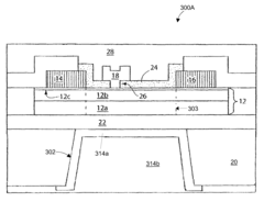
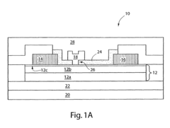
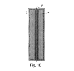
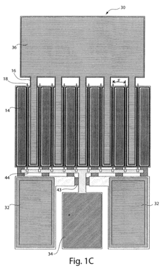
- High electron mobility transistor (HEMT) structures: Design and implementation of GaN-based high electron mobility transistors, which utilize the two-dimensional electron gas formed at the interface between GaN and AlGaN layers. These structures offer high power density, high frequency operation, and improved thermal performance for power electronics and RF applications.
- GaN substrate and crystal growth: Techniques for growing high-quality gallium nitride crystals and substrates for transistor applications. These methods address challenges in producing low-defect GaN materials through approaches such as hydride vapor phase epitaxy (HVPE), ammonothermal growth, and defect reduction strategies to improve device performance and reliability.
- GaN power transistor designs: Specialized designs for gallium nitride power transistors that focus on high voltage handling, current capacity, and switching performance. These designs incorporate features such as field plates, optimized gate structures, and novel device geometries to maximize power handling capabilities while minimizing losses.
- GaN transistor reliability and performance enhancement: Methods to improve the reliability and performance of gallium nitride transistors, including surface passivation techniques, thermal management solutions, and stress mitigation approaches. These enhancements address common failure mechanisms such as current collapse, gate leakage, and thermal degradation to extend device lifetime and stability under harsh operating conditions.
02 GaN HEMT (High Electron Mobility Transistor) structures
High Electron Mobility Transistors based on gallium nitride offer superior performance for high-frequency and high-power applications. These structures typically feature a two-dimensional electron gas (2DEG) at the interface between GaN and AlGaN layers, which provides exceptional electron mobility. Design innovations in the gate structure, channel configuration, and contact formation help optimize switching speed, power handling capability, and thermal management.Expand Specific Solutions03 Substrate materials and crystal growth for GaN devices
The choice of substrate material and crystal growth techniques significantly impacts the performance of gallium nitride transistors. Common substrates include silicon, silicon carbide, and sapphire, each offering different advantages in terms of cost, thermal conductivity, and lattice matching. Advanced crystal growth methods such as MOCVD (Metal-Organic Chemical Vapor Deposition) and HVPE (Hydride Vapor Phase Epitaxy) are employed to create high-quality GaN layers with minimal defects.Expand Specific Solutions04 Power electronics applications of GaN transistors
Gallium nitride transistors excel in power electronics applications due to their wide bandgap properties, high breakdown voltage, and low on-resistance. These characteristics enable more efficient power conversion, smaller form factors, and reduced cooling requirements compared to silicon-based alternatives. GaN transistors are increasingly used in power supplies, motor drives, renewable energy systems, and electric vehicle charging infrastructure.Expand Specific Solutions05 RF and microwave performance enhancements
Gallium nitride transistors offer exceptional performance in radio frequency (RF) and microwave applications. Design innovations focus on improving parameters such as power density, linearity, efficiency, and frequency response. Advanced structures including field plates, passivation layers, and optimized gate geometries help reduce parasitic effects and enhance reliability under high-frequency operation, making GaN transistors ideal for telecommunications, radar systems, and satellite communications.Expand Specific Solutions
Leading Companies and Research Institutions in GaN Semiconductors
The gallium nitride (GaN) transistor market is experiencing rapid growth, currently in the early mainstream adoption phase with an expanding market size driven by power electronics and RF applications. The technology has reached commercial maturity in certain segments while still evolving in others, with key players demonstrating varying levels of technological advancement. Companies like GaN Systems, MACOM, and Infineon lead in commercial deployment, while Intel, Huawei, and NXP are investing heavily in GaN integration with silicon technologies. Research institutions including MIT, Arizona State University, and China's Institute of Microelectronics are advancing fundamental material science innovations. The competitive landscape shows regional clusters forming in North America, Europe, and Asia, with Chinese companies like Huacan Optoelectronics and Innoscience rapidly expanding manufacturing capacity to challenge established Western players.
GaN Systems, Inc.
Technical Solution: GaN Systems has pioneered advanced gallium nitride transistor technology with their proprietary Island Technology® design, which features a unique cell layout that maximizes current handling capability while minimizing thermal resistance. Their GaN transistors utilize advanced material science innovations including optimized buffer layer structures and gate dielectric engineering to minimize current collapse and dynamic RDS(on) effects. The company has developed specialized surface passivation techniques to enhance reliability and stability under high-voltage switching conditions. Their transistors incorporate advanced thermal management through innovative die-attach materials and package designs that effectively dissipate heat from the GaN device. GaN Systems has also focused on material interface optimization between GaN and substrate materials to reduce defect density and improve overall device performance.
Strengths: Industry-leading power density and switching performance; proprietary design enables higher current handling in smaller form factors; excellent thermal management solutions. Weaknesses: Higher cost compared to silicon alternatives; requires specialized gate drivers; still faces challenges with long-term reliability data compared to mature silicon technologies.
Innoscience Suzhou Semiconductor Co. Ltd.
Technical Solution: Innoscience has developed a comprehensive GaN transistor technology platform based on their innovative material science approach to 8-inch GaN-on-Si wafer fabrication. Their technology focuses on precise epitaxial layer engineering with optimized AlGaN/GaN heterostructure interfaces to enhance electron mobility in the 2DEG channel. The company has pioneered advanced buffer layer designs that effectively manage strain between GaN and silicon substrates, significantly reducing defect densities and improving yield on large-diameter wafers. Innoscience's material science innovations include specialized surface treatment processes that enhance interface quality between dielectric layers and GaN, resulting in improved threshold voltage stability. Their transistors feature proprietary field plate structures designed through extensive material simulation to optimize electric field distribution and enhance breakdown voltage while maintaining low on-resistance characteristics.
Strengths: Mass production capability on 8-inch wafers enables cost-effective manufacturing; comprehensive product portfolio spanning both 650V and 100V device families; vertically integrated business model provides better quality control. Weaknesses: Relatively newer entrant compared to some established competitors; international market presence still developing; technology primarily focused on enhancement-mode devices rather than offering both depletion and enhancement options.
Key Patents and Breakthroughs in GaN Material Science
Nitride power transistor and manufacturing method thereof
PatentActiveUS20190140088A1
Innovation
- A nitride power transistor is developed with a silicon substrate featuring a differently doped semiconductor composite structure forming a space charge depletion region, combined with a nitride epitaxial layer, which increases the breakdown voltage and includes a GaN capping layer and AlN insertion layer to enhance electron mobility and reduce surface defects.
Gallium nitride material devices and thermal designs thereof
PatentActiveUS7745848B1
Innovation
- The design involves arranging transistors in cells with optimized spacing and staggered configurations, along with thermally conductive packaging and selective substrate removal to enhance heat conduction, including the use of vias and thermally conductive material regions to improve thermal resistance.
Thermal Management Innovations for GaN Devices
Thermal management represents one of the most critical challenges in the development and application of Gallium Nitride (GaN) transistors. As GaN devices operate at higher power densities and frequencies than traditional silicon-based semiconductors, they generate significant heat that must be efficiently dissipated to maintain performance and reliability. Recent innovations in thermal management for GaN devices have focused on multi-faceted approaches combining advanced materials science with novel structural designs.
Diamond-based heat spreaders have emerged as a promising solution due to diamond's exceptional thermal conductivity (approximately 2000 W/m·K), which is five times higher than copper. Chemical Vapor Deposition (CVD) techniques now enable the growth of synthetic diamond directly onto GaN substrates, creating a near-perfect thermal interface. This integration has demonstrated up to 40% reduction in peak junction temperatures in high-power GaN transistors.
Nano-engineered thermal interface materials (TIMs) represent another significant advancement. These materials incorporate carbon nanotubes, graphene, and metallic nanoparticles to enhance thermal conductivity while maintaining flexibility. Recent studies have shown that graphene-enhanced TIMs can reduce thermal resistance by up to 60% compared to conventional thermal greases when applied between GaN devices and heat sinks.
Microfluidic cooling channels integrated directly into GaN device packaging have demonstrated remarkable efficiency in heat extraction. These microscale channels allow coolant to flow in close proximity to the heat source, significantly reducing thermal resistance. Advanced designs featuring 3D-printed microfluidic networks have achieved cooling capacities exceeding 500 W/cm², enabling GaN devices to operate at their theoretical performance limits.
Phase-change materials (PCMs) specifically engineered for GaN thermal management offer another innovative approach. These materials absorb heat during the solid-to-liquid phase transition, effectively buffering temperature spikes during high-power operation cycles. Metal-organic PCMs with transition temperatures optimized for GaN operating ranges (150-200°C) have shown particular promise for applications with pulsed power requirements.
Computational thermal modeling has become increasingly sophisticated, enabling precise prediction of hotspots and thermal gradients in complex GaN device architectures. Machine learning algorithms now enhance these models by incorporating real-time operational data, allowing for dynamic thermal management strategies that adapt to changing conditions and extend device lifetime.
These thermal management innovations collectively represent a critical enabling factor for the continued advancement of GaN technology across power electronics, RF applications, and emerging quantum computing systems. As material science continues to evolve, we can expect further breakthroughs that will push the performance boundaries of GaN devices even further.
Sustainability and Environmental Impact of GaN Manufacturing
The manufacturing processes for Gallium Nitride (GaN) transistors present both significant environmental challenges and sustainability opportunities that warrant careful consideration as this technology continues to expand. GaN production traditionally requires substantial energy inputs, particularly during crystal growth processes where temperatures can exceed 1000°C. These high-temperature operations contribute to considerable carbon emissions when powered by non-renewable energy sources, raising concerns about the overall environmental footprint of GaN manufacturing.
Water usage represents another critical environmental factor, with semiconductor fabrication facilities typically consuming millions of gallons daily for cleaning and processing. GaN manufacturing is no exception, though recent innovations in closed-loop water recycling systems have demonstrated potential reductions of up to 30-40% in freshwater requirements compared to traditional semiconductor manufacturing processes.
Chemical utilization in GaN production presents additional environmental considerations. The process employs various hazardous substances including ammonia, trimethylgallium, and hydrogen, which require stringent handling protocols and waste management systems. However, the industry has made notable progress in developing less toxic precursors and more efficient chemical recovery systems that minimize environmental discharge.
From a sustainability perspective, GaN transistors offer compelling advantages that may offset manufacturing impacts. Their superior energy efficiency in end applications—particularly in power electronics—translates to significant lifetime energy savings. Research indicates that GaN-based power systems can achieve 40-50% higher efficiency than silicon alternatives in certain applications, potentially saving substantial energy over product lifespans.
Material resource efficiency also favors GaN technology. The exceptional properties of GaN allow for smaller device geometries, reducing material requirements per functional unit. Additionally, recent advances in substrate reuse techniques have demonstrated possibilities for recovering and repurposing expensive materials like sapphire substrates, potentially reducing the material intensity of manufacturing by 20-25%.
End-of-life considerations for GaN devices remain an evolving area of research. While containing valuable materials that could theoretically be recovered, current recycling infrastructure is not optimized for GaN device processing. Several research initiatives are exploring specialized recovery methods for gallium and other valuable elements from electronic waste, though commercial-scale implementation remains limited.
The industry is increasingly adopting life cycle assessment (LCA) methodologies to quantify environmental impacts across the entire value chain. These assessments typically reveal that while manufacturing impacts are significant, they may be offset by efficiency gains during the use phase, particularly in high-power applications where energy savings accumulate over years of operation.
Unlock deeper insights with Patsnap Eureka Quick Research — get a full tech report to explore trends and direct your research. Try now!
Generate Your Research Report Instantly with AI Agent
Supercharge your innovation with Patsnap Eureka AI Agent Platform!