Research on the Impact of Industry Standards on Gallium Nitride Transistors
OCT 14, 202510 MIN READ
Generate Your Research Report Instantly with AI Agent
Patsnap Eureka helps you evaluate technical feasibility & market potential.
GaN Transistor Standards Evolution and Objectives
Gallium Nitride (GaN) transistor technology has evolved significantly over the past three decades, transitioning from laboratory curiosity to commercial reality. The development of this wide bandgap semiconductor technology began in the early 1990s with fundamental research into material properties and basic device structures. By the early 2000s, researchers had demonstrated the first viable GaN high electron mobility transistors (HEMTs), showcasing their potential for high-frequency, high-power applications.
The evolution of GaN transistor technology has been marked by several key milestones. Initially, the focus was on military and aerospace applications due to high production costs. However, as manufacturing techniques improved and costs decreased, GaN transistors began penetrating commercial markets around 2010, particularly in telecommunications infrastructure and power conversion systems. Recent years have witnessed accelerated adoption in consumer electronics, automotive systems, and renewable energy applications.
Industry standards have played a crucial role in this technological progression. Early standardization efforts primarily addressed material quality and reliability concerns, as GaN devices initially suffered from various failure mechanisms including current collapse and gate leakage. The JEDEC JC-70 committee, formed in 2017, marked a significant turning point by establishing the first comprehensive standards specifically for GaN power devices.
The objectives of GaN transistor standardization efforts are multifaceted. First, they aim to establish uniform testing methodologies that enable fair comparison between devices from different manufacturers. This includes standardized procedures for measuring key parameters such as on-resistance, switching performance, and thermal characteristics under realistic operating conditions.
Second, standards seek to define reliability qualification frameworks tailored to GaN's unique properties and failure modes, which differ significantly from silicon devices. These frameworks help ensure that GaN transistors meet the stringent reliability requirements of mission-critical applications.
Third, standardization efforts focus on establishing application-specific guidelines that facilitate the integration of GaN technology into various systems. This includes defining interface specifications, driving requirements, and thermal management considerations that enable designers to effectively utilize GaN's superior performance characteristics.
Looking forward, emerging standardization objectives include addressing new GaN device architectures such as vertical GaN transistors, establishing standards for integrated GaN systems-on-chip, and developing frameworks for GaN-specific packaging technologies that optimize thermal performance and parasitic effects. Additionally, there is growing emphasis on standardizing GaN device models for circuit simulation to accelerate design cycles and improve first-pass success rates.
The continued evolution of these standards is expected to play a pivotal role in expanding GaN transistor adoption across diverse application domains, ultimately enabling this technology to reach its full potential in revolutionizing power electronics and RF systems.
Market Demand Analysis for Standardized GaN Devices
The global market for Gallium Nitride (GaN) transistors has experienced significant growth in recent years, driven primarily by increasing demand for high-performance power electronics across multiple industries. Market research indicates that the GaN power device market is projected to grow at a compound annual growth rate of 22% through 2026, reaching approximately $1.8 billion. This robust growth trajectory underscores the critical importance of industry standardization to support market expansion.
Standardized GaN devices are increasingly sought after in telecommunications infrastructure, particularly with the ongoing global deployment of 5G networks. Network equipment manufacturers require consistent performance parameters and reliability benchmarks that only standardized components can provide. The telecommunications sector alone accounts for nearly 30% of the current GaN device market demand, with this percentage expected to increase as network densification continues.
Consumer electronics represents another significant market segment driving demand for standardized GaN solutions. Fast-charging technologies for mobile devices and laptops have created a surge in demand for compact, efficient power adapters. Major consumer electronics manufacturers have begun incorporating GaN-based charging solutions, but cite the lack of uniform standards as a barrier to wider adoption. Industry surveys reveal that 78% of electronics manufacturers would increase their GaN implementation if comprehensive standards were established.
The automotive sector presents perhaps the most promising long-term growth opportunity for standardized GaN devices. Electric vehicle (EV) manufacturers are actively seeking more efficient power conversion solutions to extend range and reduce charging times. The demand for onboard chargers and DC-DC converters that meet automotive-grade reliability standards is projected to grow by 35% annually through 2028. However, automotive tier-one suppliers consistently identify the lack of uniform qualification standards as the primary obstacle to widespread GaN adoption in vehicle systems.
Industrial applications, including motor drives, renewable energy inverters, and factory automation systems, collectively represent a substantial market for standardized GaN devices. These applications demand proven reliability under harsh operating conditions, with clearly defined performance parameters across temperature ranges and load profiles. The industrial sector currently accounts for approximately 25% of GaN device demand but faces adoption challenges due to fragmented specification approaches among different manufacturers.
Defense and aerospace applications, while smaller in volume, drive significant value in the GaN market due to their demanding performance requirements and higher price tolerance. These sectors require standardized radiation-hardened components with consistent reliability characteristics, creating a specialized but lucrative market segment estimated at $220 million annually.
The establishment of comprehensive industry standards would address current market fragmentation and accelerate adoption across all these sectors. Market analysis indicates that standardization could potentially unlock an additional $500 million in annual market value by 2025 through reduced qualification costs, improved supply chain efficiency, and accelerated design cycles.
Current Standardization Challenges in GaN Technology
Despite significant advancements in GaN transistor technology, standardization remains a critical challenge impeding widespread industry adoption. Current standards for silicon-based semiconductors are inadequate for GaN devices due to fundamental differences in material properties, operating conditions, and reliability mechanisms. This standardization gap creates uncertainty for manufacturers and end-users alike, hindering market growth and technology integration.
A primary challenge is the lack of unified testing protocols for GaN reliability assessment. Unlike silicon, GaN devices exhibit unique failure mechanisms such as dynamic RON, current collapse, and buffer trapping effects that require specialized testing methodologies. Different manufacturers employ proprietary testing procedures, making performance comparisons difficult and complicating qualification processes for system designers.
Thermal management standardization presents another significant hurdle. GaN's superior thermal conductivity enables higher power densities, but also necessitates novel thermal characterization and management approaches. Current thermal resistance measurement standards developed for silicon devices fail to account for GaN's unique thermal behavior, particularly in high-frequency switching applications where transient thermal effects become critical.
Safety certification standards also lag behind GaN technology development. Regulatory bodies like UL, IEC, and JEDEC are still adapting their frameworks to accommodate GaN's higher operating voltages, faster switching speeds, and different insulation requirements. This regulatory uncertainty increases compliance costs and extends time-to-market for GaN-based products.
Application-specific standards represent another gap. While power conversion applications have received some standardization attention, emerging GaN applications in RF, automotive, and aerospace domains lack comprehensive standards frameworks. This absence particularly affects interoperability between GaN devices from different manufacturers, limiting design flexibility and increasing integration costs.
Intellectual property fragmentation further complicates standardization efforts. Key GaN technologies are protected by patents held by various entities, creating potential barriers to establishing open industry standards. Standard-essential patents must be identified and licensing frameworks established to prevent IP issues from impeding standardization progress.
International harmonization of standards remains elusive, with different regional approaches emerging in North America, Europe, and Asia. This fragmentation creates compliance challenges for global manufacturers and may lead to market segmentation. Coordinating efforts between standards organizations like IEEE, JEDEC, IEC, and regional bodies is essential but progressing slowly due to competing interests and technical complexities.
Current Industry Standards Implementation Approaches
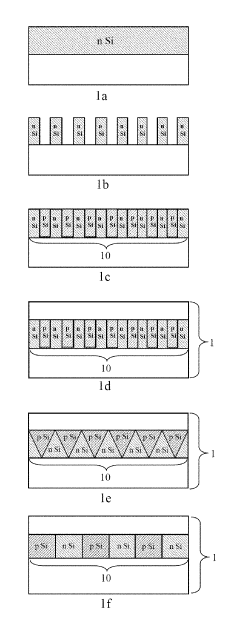
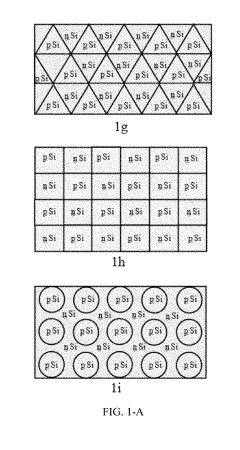
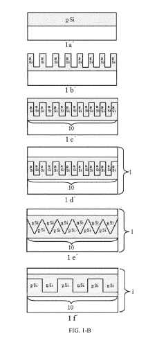
01 Fabrication methods for GaN transistors
Various fabrication techniques are employed to create high-performance gallium nitride transistors. These methods include epitaxial growth processes, substrate preparation, and specialized deposition techniques that enhance the crystalline quality of the GaN layers. Advanced manufacturing approaches help reduce defects and improve the electrical characteristics of the resulting transistors, enabling better performance in high-power and high-frequency applications.- Fabrication methods for GaN transistors: Various methods for manufacturing gallium nitride transistors, including epitaxial growth techniques, substrate preparation, and device fabrication processes. These methods focus on improving crystal quality, reducing defects, and enhancing device performance. Specific approaches include MOCVD growth, selective area growth, and specialized etching techniques to create high-quality GaN layers for transistor applications.
- GaN HEMT structures and designs: High Electron Mobility Transistor (HEMT) structures based on gallium nitride, featuring various layer compositions and device architectures. These designs typically include AlGaN/GaN heterojunctions that create a two-dimensional electron gas (2DEG) for high-speed operation. Advanced HEMT designs incorporate field plates, specialized gate structures, and buffer layers to enhance breakdown voltage, reduce leakage current, and improve thermal performance.
- GaN substrate and crystal growth technology: Technologies for growing high-quality gallium nitride crystals and substrates for transistor applications. These methods address challenges in producing low-defect GaN materials, including techniques for reducing threading dislocations, controlling crystal orientation, and scaling up crystal size. Approaches include hydride vapor phase epitaxy (HVPE), ammonothermal growth, and specialized techniques for managing strain in epitaxial layers.
- GaN power transistor designs: Specialized gallium nitride transistor designs optimized for power applications, featuring high breakdown voltage, low on-resistance, and enhanced thermal management. These designs incorporate field plates, specialized gate structures, passivation layers, and other features to handle high voltages and currents while maintaining reliability. Various approaches to managing electric fields and enhancing current handling capabilities are implemented to maximize power density.
- GaN-based optoelectronic and RF devices: Integration of gallium nitride transistors with optoelectronic components and radio frequency (RF) applications. These designs combine the high-frequency capabilities of GaN transistors with light-emitting or light-detecting functions, or optimize them specifically for RF performance. Approaches include monolithic integration of transistors with LEDs or photodetectors, and specialized designs for high-frequency operation in communication systems.
02 GaN HEMT (High Electron Mobility Transistor) structures
High Electron Mobility Transistors based on gallium nitride utilize a two-dimensional electron gas (2DEG) formed at the interface between GaN and AlGaN layers. This structure enables high electron mobility and fast switching speeds. Design innovations in the gate structure, channel formation, and contact metallization help optimize performance characteristics such as breakdown voltage, on-resistance, and switching frequency, making these devices suitable for power electronics applications.Expand Specific Solutions03 GaN substrate and crystal growth technology
The quality of gallium nitride substrates significantly impacts transistor performance. Advanced crystal growth techniques, including HVPE (Hydride Vapor Phase Epitaxy), MOCVD (Metal-Organic Chemical Vapor Deposition), and ammono-thermal methods, are used to produce high-quality GaN substrates with minimal defects. These substrates provide the foundation for creating transistors with superior electrical properties and reliability for demanding applications.Expand Specific Solutions04 GaN power transistor designs
Gallium nitride power transistors are designed to handle high voltages and currents while maintaining efficiency. Specific design features include field plates for enhanced breakdown voltage, specialized gate structures to reduce leakage current, and thermal management solutions. These designs enable GaN transistors to operate at higher frequencies and temperatures than silicon-based alternatives, making them ideal for power conversion applications in automotive, industrial, and renewable energy systems.Expand Specific Solutions05 GaN-based optoelectronic and RF devices
Beyond power applications, gallium nitride transistors are utilized in optoelectronic and radio frequency (RF) devices. These applications leverage GaN's wide bandgap properties to create high-frequency amplifiers, laser diodes, and LED structures. Special design considerations for these applications include optimized heterostructures, surface passivation techniques, and specialized contact formations that enhance performance in communication systems, radar technology, and lighting applications.Expand Specific Solutions
Key Industry Players and Standards Organizations
The gallium nitride (GaN) transistor industry is currently in a growth phase, with market size expanding rapidly due to increasing demand in power electronics, telecommunications, and automotive sectors. Industry standards play a crucial role in this evolving landscape, driving technological maturity and market adoption. Key players like Infineon Technologies, GaN Systems, and MACOM are leading commercial deployment, while companies such as Huawei, Intel, and Texas Instruments are investing heavily in R&D to overcome technical challenges. Academic institutions including Arizona State University and research organizations like CEA are contributing to standardization efforts. Chinese manufacturers like HC Semitek and Suzhou Jingzhan Semiconductor are rapidly advancing in GaN epitaxial materials, challenging established players and potentially reshaping the competitive landscape through standards compliance.
Huawei Technologies Co., Ltd.
Technical Solution: Huawei has developed a unique approach to GaN standardization focused primarily on telecommunications infrastructure applications. Their work includes creating standardized GaN-based power amplifier modules for 5G base stations that have influenced industry specifications for efficiency and power density. Huawei has established internal standards for GaN implementation that address reliability concerns specific to telecom environments, including thermal cycling, humidity resistance, and long-term stability requirements. These standards have subsequently been shared with industry partners and suppliers, creating de facto standards in the telecom sector. The company has also pioneered standardized testing methodologies for GaN RF performance that account for the specific operational conditions of modern communications systems. Huawei's standardization efforts extend to system-level integration, where they've developed reference architectures for implementing GaN technology in power delivery networks for data centers and telecommunications equipment. Their work has particularly focused on standardizing the interface between GaN devices and digital control systems.
Strengths: Leading position in telecommunications applications of GaN; strong vertical integration allowing for comprehensive standards development; significant influence in Asian markets and standards bodies. Weaknesses: Limited influence in some Western markets due to geopolitical factors; standards work is heavily focused on telecommunications rather than broader GaN applications; less public sharing of standards development compared to some competitors.
Analog Devices, Inc.
Technical Solution: Analog Devices has focused their GaN standardization efforts on precision applications and mixed-signal integration. Their approach centers on standardizing the interface between GaN power devices and precision analog control systems, creating reference designs that establish benchmarks for performance in applications requiring high accuracy. ADI has been particularly active in developing standards for GaN implementation in instrumentation, aerospace, defense, and high-reliability industrial applications. Their work includes standardized testing methodologies that address the unique characteristics of GaN in precision circuits, including dynamic performance parameters and electromagnetic compatibility considerations. ADI has contributed to industry standards committees focusing on reliability qualification and testing procedures specific to GaN technology. The company has developed standardized design methodologies that help engineers implement GaN solutions with predictable performance across varying operating conditions. Their standardization efforts extend to system-level considerations, including power management architectures and thermal solutions optimized for GaN technology.
Strengths: Deep expertise in precision analog that brings unique perspective to GaN standards; strong position in high-reliability markets that demand rigorous standardization; comprehensive approach to system-level standards. Weaknesses: More focused on specialized applications rather than high-volume consumer or automotive markets; standards development sometimes emphasizes performance parameters that are less relevant to mainstream GaN applications.
Critical Standards and Specifications Analysis
Gallium nitride material transistors and methods associated with the same
PatentInactiveUS7994540B2
Innovation
- The development of gallium nitride material transistors with active regions formed in a gallium nitride layer, integrated with a matching circuit to transform impedance, enabling the amplification of input signals to produce output signals with an adjacent channel power ratio (ACPR) of less than or equal to −20 dBc, while maintaining high drain efficiencies and output powers.
Nitride power transistor and manufacturing method thereof
PatentActiveUS20190140088A1
Innovation
- A nitride power transistor is developed with a silicon substrate featuring a differently doped semiconductor composite structure forming a space charge depletion region, combined with a nitride epitaxial layer, which increases the breakdown voltage and includes a GaN capping layer and AlN insertion layer to enhance electron mobility and reduce surface defects.
Interoperability and Compatibility Considerations
Interoperability and compatibility represent critical considerations in the adoption and implementation of Gallium Nitride (GaN) transistor technology across various industries. As industry standards continue to evolve, ensuring seamless integration between GaN devices and existing silicon-based systems remains a significant challenge for manufacturers and system designers.
The heterogeneous integration of GaN transistors with conventional silicon technologies necessitates careful attention to interface specifications, signal levels, and driving requirements. Current industry standards such as JEDEC, AEC-Q101 for automotive applications, and IPC standards for PCB design must be adapted or extended to accommodate the unique electrical characteristics of GaN devices, including faster switching speeds and different thermal profiles.
Cross-platform compatibility issues emerge when GaN transistors are implemented in systems originally designed for silicon MOSFETs or IGBTs. The significantly different gate drive requirements, threshold voltages, and switching behaviors of GaN devices often require modifications to driver circuits and control systems. This compatibility gap has prompted several industry consortia to develop specialized interface standards and reference designs specifically tailored for GaN implementation.
Interoperability between different manufacturers' GaN devices presents another layer of complexity. Unlike the mature silicon ecosystem, GaN transistor specifications and performance characteristics can vary substantially between vendors, complicating second-sourcing strategies essential for supply chain resilience. Organizations such as the JEDEC JC-70 Wide Bandgap Power Electronic Conversion Semiconductors committee are working to establish standardized testing methodologies and parameter definitions to improve cross-vendor compatibility.
System-level interoperability extends beyond the transistor itself to encompass packaging standards, thermal management interfaces, and electromagnetic compatibility considerations. The higher operating frequencies enabled by GaN technology can introduce electromagnetic interference challenges that may conflict with existing EMC standards, requiring careful system design and potentially updated regulatory frameworks.
Looking forward, the development of comprehensive design libraries, simulation models, and standardized characterization methods will be crucial for improving the interoperability landscape. Industry collaboration through standards bodies and open technical forums will play a vital role in addressing these challenges, potentially accelerating GaN adoption across multiple application domains from power conversion to RF communications.
The establishment of clear migration paths from silicon to GaN technologies, supported by appropriate standards and design guidelines, will ultimately determine how quickly industries can leverage the performance advantages of GaN while maintaining backward compatibility with existing systems and infrastructure.
Environmental and Safety Compliance Requirements
The environmental and safety compliance landscape for Gallium Nitride (GaN) transistors is becoming increasingly complex as industry standards evolve to address the unique properties of this semiconductor material. GaN transistors, while offering superior performance characteristics compared to silicon-based alternatives, present distinct environmental and safety challenges throughout their lifecycle that must be addressed through comprehensive regulatory frameworks.
Manufacturing processes for GaN transistors involve potentially hazardous materials, including gallium and nitrogen compounds, which are subject to strict handling protocols under regulations such as the European Union's Registration, Evaluation, Authorization and Restriction of Chemicals (REACH) and the Restriction of Hazardous Substances (RoHS) Directive. These standards impose specific limits on toxic substances and mandate detailed documentation of material composition, significantly impacting manufacturing processes and supply chain management for GaN transistor producers.
Thermal management during operation represents another critical compliance area, as GaN transistors can operate at higher temperatures than silicon-based counterparts. Industry standards such as those developed by the International Electrotechnical Commission (IEC) and Underwriters Laboratories (UL) establish safety thresholds for thermal performance, requiring manufacturers to implement robust cooling solutions and thermal protection mechanisms to prevent overheating risks in end applications.
Electromagnetic compatibility (EMC) standards have also been adapted to address the unique switching characteristics of GaN transistors. Their faster switching speeds can generate electromagnetic interference that exceeds traditional silicon-based parameters, necessitating compliance with updated EMC standards such as IEC 61000 series and CISPR requirements. These standards ensure that GaN-based systems do not disrupt nearby electronic equipment while maintaining their performance advantages.
End-of-life considerations for GaN transistors are governed by waste electrical and electronic equipment (WEEE) regulations, which mandate responsible recycling practices. The presence of gallium, classified as a critical raw material in many jurisdictions, has prompted the development of specialized recovery processes to extract and reuse this valuable element from discarded GaN devices, aligning with circular economy principles increasingly embedded in environmental compliance requirements.
Occupational safety standards for facilities manufacturing or processing GaN transistors have evolved to address potential respiratory hazards associated with gallium nitride particulates. Organizations such as the Occupational Safety and Health Administration (OSHA) and the National Institute for Occupational Safety and Health (NIOSH) have established exposure limits and recommended control measures to protect workers involved in GaN transistor production and handling.
As GaN technology continues to penetrate new markets, particularly in automotive and medical applications, compliance with industry-specific standards such as ISO 26262 for functional safety in automotive electronics and IEC 60601 for medical electrical equipment becomes essential for manufacturers seeking to expand their market presence while ensuring regulatory compliance.
Unlock deeper insights with Patsnap Eureka Quick Research — get a full tech report to explore trends and direct your research. Try now!
Generate Your Research Report Instantly with AI Agent
Supercharge your innovation with Patsnap Eureka AI Agent Platform!