How Emerging Applications are Shaping Gallium Nitride Transistor Innovation
OCT 14, 202510 MIN READ
Generate Your Research Report Instantly with AI Agent
Patsnap Eureka helps you evaluate technical feasibility & market potential.
GaN Transistor Evolution and Innovation Objectives
Gallium Nitride (GaN) transistor technology has undergone significant evolution since its inception in the early 1990s. Initially developed for optoelectronic applications, GaN transistors have progressively expanded into power electronics due to their superior material properties compared to silicon. The wide bandgap nature of GaN (3.4 eV versus 1.1 eV for silicon) enables higher breakdown voltages, faster switching speeds, and operation at elevated temperatures, making it an ideal candidate for next-generation power applications.
The technological trajectory of GaN transistors has been marked by several breakthrough innovations. Early development focused on addressing fundamental challenges such as substrate compatibility, defect density reduction, and reliable gate structures. The introduction of AlGaN/GaN heterojunction structures in the late 1990s represented a pivotal advancement, enabling the creation of high electron mobility transistors (HEMTs) with exceptional performance characteristics.
Recent years have witnessed accelerated innovation in GaN transistor technology, driven primarily by emerging applications in electric vehicles, renewable energy systems, data centers, and 5G infrastructure. These applications demand higher efficiency, power density, and reliability than traditional silicon-based solutions can provide. The push toward miniaturization and energy efficiency has further catalyzed GaN transistor development, with significant improvements in current handling capability, switching performance, and thermal management.
The primary innovation objectives for GaN transistors currently center around several key areas. Cost reduction remains paramount, as the price premium over silicon devices continues to limit widespread adoption. This involves developing more efficient manufacturing processes, exploring alternative substrates beyond expensive silicon carbide and sapphire, and scaling production volumes to achieve economies of scale.
Reliability enhancement constitutes another critical objective, particularly for applications requiring extended operational lifetimes. Research efforts are focused on mitigating current collapse phenomena, improving gate stability, and developing more robust passivation techniques to ensure consistent performance under various environmental conditions.
Integration capabilities represent a third major innovation target. The development of monolithically integrated GaN power ICs that combine power transistors with control and protection circuitry on a single chip promises to revolutionize power conversion systems. This approach aims to minimize parasitic elements, improve thermal performance, and reduce overall system size and cost.
Looking forward, the innovation roadmap for GaN transistors is increasingly being shaped by application-specific requirements. The automotive sector is driving development of higher voltage (>1200V) GaN devices with enhanced robustness. Simultaneously, consumer electronics applications are pushing for ultra-compact, highly integrated solutions operating at lower voltages but with exceptional efficiency profiles.
Market Demand Analysis for GaN-Based Power Solutions
The global market for Gallium Nitride (GaN) power solutions is experiencing unprecedented growth, driven primarily by the increasing demand for high-efficiency power electronics across multiple industries. Current market valuations place the GaN power device market at approximately $1.4 billion in 2023, with projections indicating a compound annual growth rate (CAGR) of 25% through 2028, potentially reaching $4.3 billion by the end of the forecast period.
This remarkable growth trajectory is fueled by several key market demands. The automotive sector represents one of the most significant drivers, particularly with the rapid expansion of electric vehicles (EVs). GaN-based power solutions offer superior power density and efficiency compared to traditional silicon-based alternatives, enabling faster charging capabilities, extended range, and reduced weight in EV power systems. Industry analysts report that EV manufacturers are increasingly adopting GaN technology for onboard chargers and DC-DC converters, with adoption rates increasing by 35% annually.
Consumer electronics constitutes another substantial market segment for GaN power solutions. The persistent consumer demand for smaller, lighter, and more efficient charging solutions has created a fertile ground for GaN technology. Major smartphone and laptop manufacturers have begun incorporating GaN-based chargers, reducing form factors by up to 40% while delivering equivalent or superior charging performance. This trend is expected to accelerate as consumers increasingly prioritize fast-charging capabilities and portable power solutions.
The telecommunications and data center sectors present additional high-growth opportunities for GaN power solutions. With the ongoing deployment of 5G infrastructure and the exponential growth in data processing requirements, power efficiency has become a critical consideration. GaN-based power supplies can reduce energy consumption in these applications by 15-20% compared to silicon alternatives, translating to significant operational cost savings at scale.
Renewable energy systems represent an emerging but rapidly growing application area for GaN technology. Solar inverters and wind power converters benefit substantially from GaN's higher switching frequencies and reduced power losses. Market research indicates that GaN adoption in renewable energy applications is growing at 30% annually, outpacing the overall market growth rate.
Regional analysis reveals that Asia-Pacific currently dominates the GaN power solutions market, accounting for approximately 45% of global demand, followed by North America (30%) and Europe (20%). However, the fastest growth is occurring in emerging markets, particularly in countries investing heavily in renewable energy infrastructure and electric mobility solutions.
GaN Technology Status and Development Barriers
Gallium Nitride (GaN) transistor technology has witnessed significant advancements globally, yet continues to face substantial technical challenges that impede its widespread adoption. Currently, GaN transistors have established a strong presence in high-frequency RF applications and power electronics, with commercial products available across various voltage ranges from 100V to 900V. The technology demonstrates superior performance metrics compared to silicon-based alternatives, including higher switching frequencies, reduced on-resistance, and enhanced thermal conductivity.
Despite these advantages, several critical barriers persist in GaN technology development. Material quality remains a fundamental challenge, with defect densities in GaN epitaxial layers still higher than ideal, particularly when grown on non-native substrates like silicon. These defects contribute to reliability concerns and performance degradation under high-stress operating conditions. The industry continues to struggle with achieving consistent, high-yield manufacturing processes that can maintain quality while reducing production costs.
Thermal management represents another significant hurdle for GaN transistor innovation. While GaN inherently offers better thermal properties than silicon, the high power densities achievable in GaN devices create localized hotspots that can compromise long-term reliability. Current packaging technologies often fail to adequately address these thermal challenges, limiting the full performance potential of GaN transistors in high-power applications.
Device design optimization presents ongoing challenges, particularly in achieving normally-off (enhancement-mode) operation without sacrificing performance. Various approaches including p-GaN gates, recessed gates, and hybrid structures have emerged, but each introduces trade-offs between threshold voltage stability, manufacturing complexity, and overall device performance. The lack of standardization across these design approaches further complicates industry adoption.
Reliability testing and qualification standards specific to GaN technology remain underdeveloped compared to mature silicon technologies. The unique failure mechanisms in GaN devices, including dynamic on-resistance increase, current collapse phenomena, and gate leakage degradation, require specialized testing protocols that are still evolving. This uncertainty creates hesitation among system designers considering GaN for critical applications.
The geographical distribution of GaN technology development shows concentration in North America, Europe, Japan, and increasingly China. Each region has developed specialized expertise in different aspects of the technology, with Japan leading in material quality, Europe in device design innovation, and the US in high-frequency applications. This distribution creates both collaborative opportunities and competitive challenges in the global market.
Cost remains perhaps the most significant barrier to widespread GaN adoption. While performance advantages are clear, the price premium over silicon alternatives continues to limit market penetration beyond high-end applications where performance justifies the cost. Achieving economies of scale through increased production volumes represents a chicken-and-egg problem that the industry continues to navigate.
Current GaN Transistor Design Approaches
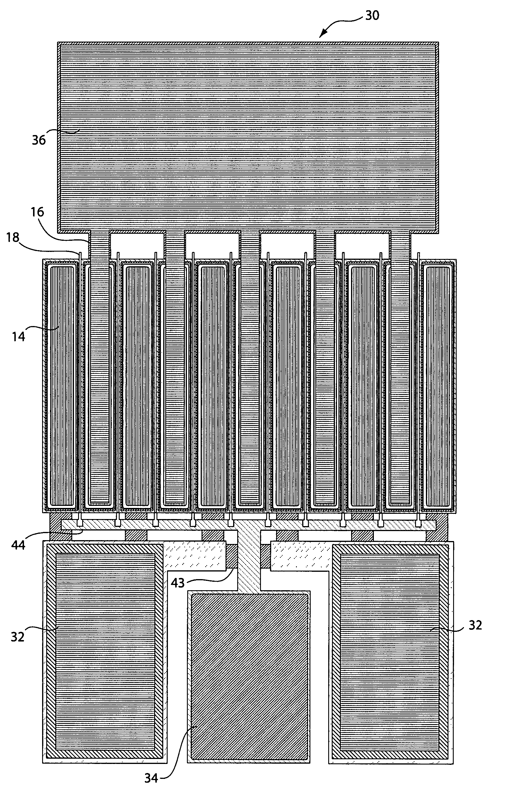
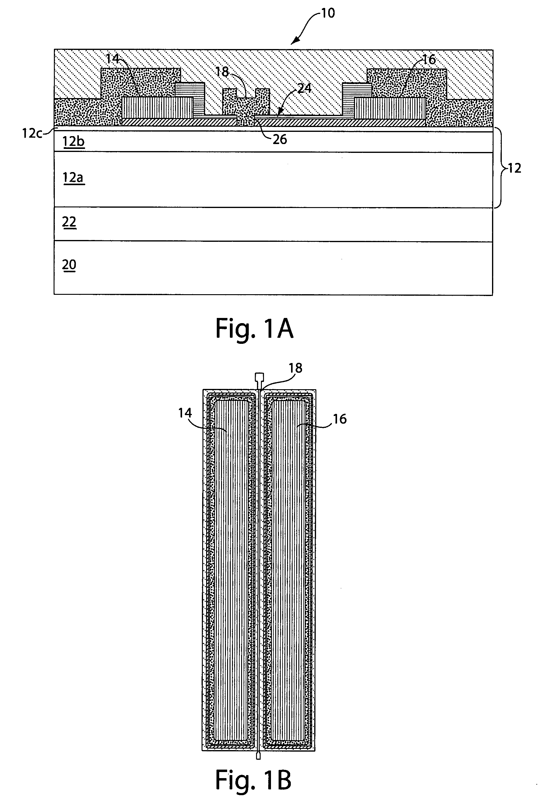
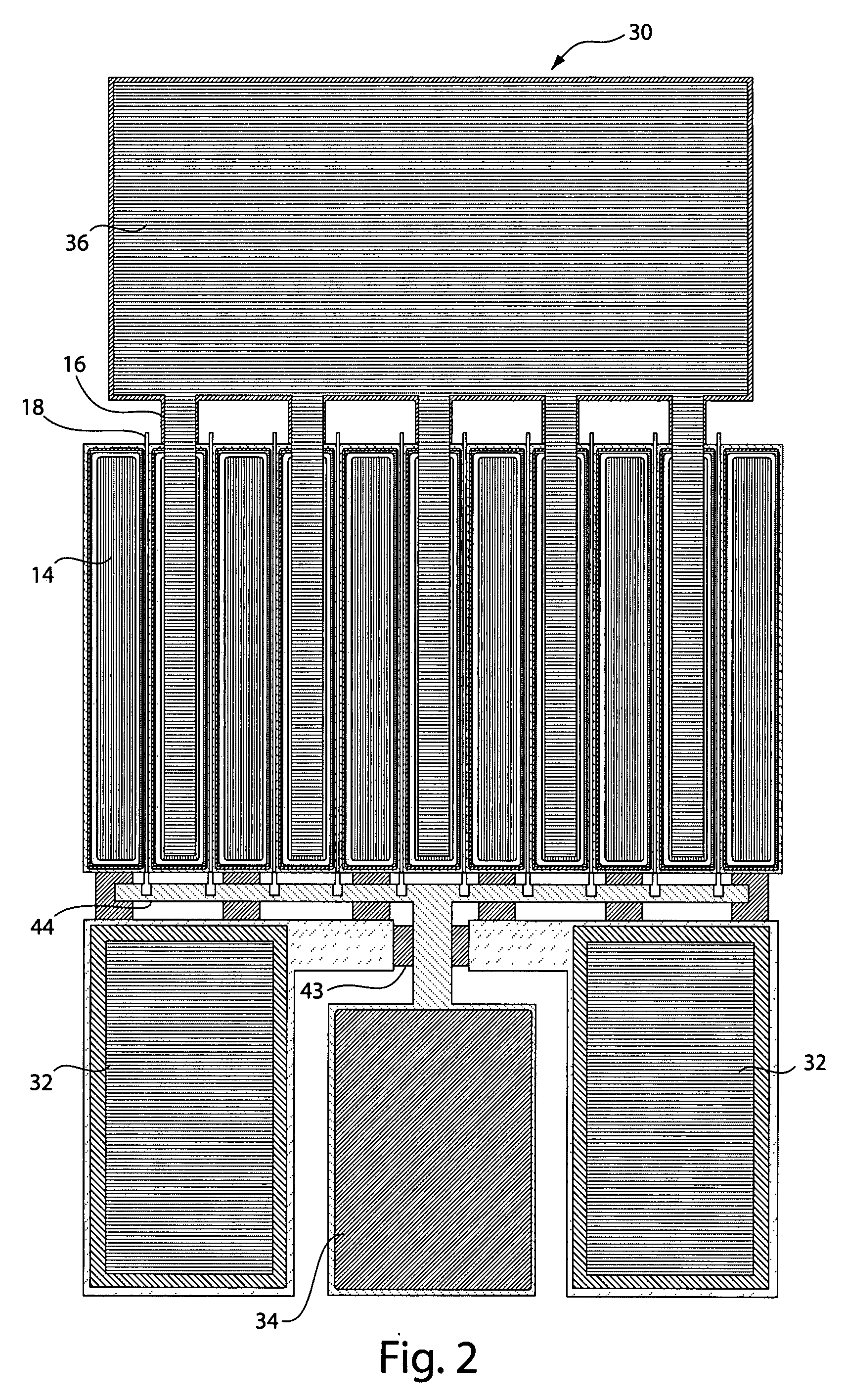
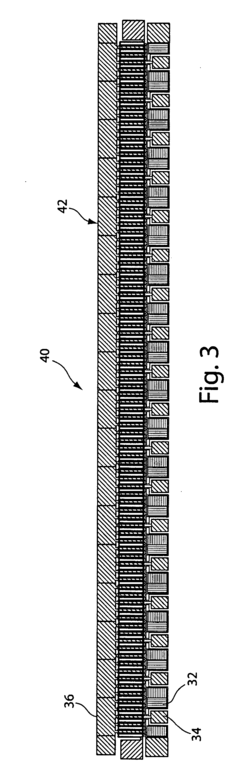
01 GaN Transistor Fabrication Techniques
Advanced fabrication methods for gallium nitride transistors involve specialized growth techniques to create high-quality GaN layers. These techniques include molecular beam epitaxy and metal-organic chemical vapor deposition to achieve optimal crystal structure. Innovations in this area focus on reducing defect density and improving uniformity of GaN layers, which directly impacts transistor performance and reliability.- GaN Transistor Fabrication Techniques: Advanced fabrication methods for gallium nitride transistors involve innovative substrate preparation, epitaxial growth processes, and device structure optimization. These techniques focus on improving crystal quality, reducing defect density, and enhancing electrical performance. Key innovations include novel MOCVD growth parameters, specialized etching processes, and advanced doping techniques that collectively contribute to higher performance GaN transistors with improved reliability and efficiency.
- High Electron Mobility Transistor (HEMT) Designs: Innovations in GaN HEMT designs focus on optimizing the heterostructure interfaces, gate configurations, and channel properties to achieve superior electron mobility and power handling capabilities. These designs incorporate novel barrier layers, field plates, and passivation techniques to mitigate current collapse and enhance breakdown voltage. Advanced HEMT architectures enable higher frequency operation, improved thermal management, and reduced on-resistance, making them ideal for high-power and high-frequency applications.
- Thermal Management Solutions: Innovative thermal management approaches for GaN transistors address the challenge of heat dissipation in high-power density devices. These solutions include advanced packaging techniques, integrated heat spreaders, and novel substrate materials with enhanced thermal conductivity. Improved thermal interfaces and optimized device geometries help to reduce thermal resistance and hot spots, enabling GaN transistors to operate reliably at higher power levels without performance degradation or reduced lifetime.
- GaN-on-Silicon Integration: Techniques for integrating GaN transistors on silicon substrates represent a significant innovation that enables cost-effective mass production. These approaches overcome lattice mismatch and thermal expansion coefficient differences through specialized buffer layers, strain management techniques, and novel growth processes. GaN-on-Si technology facilitates the integration of GaN power devices with conventional silicon-based electronics, opening new possibilities for hybrid systems and reducing the overall cost of GaN transistor implementation.
- Enhancement-Mode GaN Transistor Technology: Enhancement-mode (normally-off) GaN transistor innovations focus on creating devices that require positive gate voltage for operation, improving safety and compatibility with existing driver circuits. These technologies include recessed gate structures, p-type gate layers, hybrid MIS gate configurations, and innovative threshold voltage control methods. Enhancement-mode designs simplify circuit design, reduce power consumption, and enable more efficient power conversion systems while maintaining the performance advantages of GaN technology.
02 High Electron Mobility Transistor (HEMT) Designs
Innovations in GaN HEMT designs focus on enhancing electron mobility and reducing channel resistance. These designs typically incorporate AlGaN/GaN heterostructures to create a two-dimensional electron gas at the interface. Advanced HEMT structures include field plates, optimized gate geometries, and novel barrier layers to improve breakdown voltage, reduce leakage current, and enhance overall performance for high-frequency and high-power applications.Expand Specific Solutions03 Thermal Management Solutions
Thermal management is critical for GaN transistors operating at high power densities. Innovations include advanced substrate materials like silicon carbide that offer superior thermal conductivity compared to silicon. Other approaches involve novel heat dissipation structures, integrated cooling channels, and optimized device layouts to minimize thermal resistance. These solutions help maintain device reliability and performance under high-power operation conditions.Expand Specific Solutions04 Integration with Silicon Technology
Integrating GaN transistors with conventional silicon technology enables cost-effective manufacturing while leveraging GaN's superior properties. Innovations in this area include buffer layer engineering to accommodate lattice mismatch between GaN and silicon, selective area growth techniques, and novel bonding methods. These approaches facilitate the creation of hybrid circuits that combine the high-frequency and high-power capabilities of GaN with the maturity and cost advantages of silicon technology.Expand Specific Solutions05 Reliability Enhancement Techniques
Improving the reliability of GaN transistors involves addressing specific degradation mechanisms such as current collapse and gate leakage. Innovations include surface passivation techniques, field plate optimizations, and novel dielectric materials for gate insulation. Advanced characterization methods help identify failure modes, while stress testing protocols validate long-term reliability. These techniques collectively extend device lifetime and stability under extreme operating conditions.Expand Specific Solutions
Leading Companies in GaN Semiconductor Industry
The gallium nitride (GaN) transistor market is experiencing rapid growth, currently transitioning from early adoption to mainstream implementation across multiple sectors. The competitive landscape features established semiconductor giants like Intel, Analog Devices, and Taiwan Semiconductor Manufacturing Co. alongside GaN specialists such as GaN Systems and Transphorm Technology. Academic institutions including Xidian University and Peking University are driving fundamental research, while companies like Innoscience and NXP are commercializing innovative applications. The market is characterized by increasing technological maturity in power electronics, with recent advancements focusing on higher efficiency, smaller form factors, and enhanced thermal performance. As applications expand in electric vehicles, renewable energy, and 5G infrastructure, competition is intensifying between traditional silicon-based solutions and emerging GaN technologies.
GaN Systems, Inc.
Technical Solution: GaN Systems has pioneered innovative gallium nitride transistor technology specifically designed for emerging applications. Their Island Technology® platform features a proprietary cell layout that maximizes current handling capability while minimizing thermal resistance. The company's GaNPX® packaging eliminates wire bonds, reducing parasitic inductance and enabling higher switching frequencies up to 100MHz - significantly outperforming silicon alternatives. Their latest Gen4 GaN power transistors achieve 20% lower on-resistance and 50% lower gate charge than previous generations, enabling power densities exceeding 10kW/L in applications like electric vehicle chargers and data center power supplies. GaN Systems has also developed specialized GaN transistors for RF applications operating at frequencies up to 6GHz with high linearity and efficiency for 5G infrastructure and radar systems.
Strengths: Industry-leading power density and switching performance; proprietary packaging technology reduces parasitic effects; comprehensive design ecosystem including simulation tools and reference designs. Weaknesses: Higher cost compared to silicon alternatives; requires specialized gate drivers; thermal management challenges in high-power applications.
International Rectifier Corp.
Technical Solution: International Rectifier (now part of Infineon Technologies) pioneered GaN-on-silicon technology with their GaNpowIR® platform, which integrates enhancement-mode GaN transistors with silicon-based control and protection circuits. Their approach features a unique gate structure that achieves normally-off operation without requiring a cascode configuration, simplifying implementation while delivering superior switching performance. IR's GaN devices achieve switching frequencies exceeding 1MHz with significantly reduced switching losses compared to silicon alternatives, enabling higher efficiency and power density in applications like server power supplies and renewable energy systems. The company has developed specialized GaN solutions for automotive applications, including 100V and 600V devices optimized for onboard chargers and DC-DC converters in electric vehicles, achieving power densities up to 4kW/L while meeting stringent automotive reliability requirements.
Strengths: Integration with silicon control circuits simplifies implementation; established manufacturing infrastructure and quality systems; strong automotive qualification expertise. Weaknesses: Less competitive RDS(on) × area performance compared to newer GaN technologies; limited high-frequency capability compared to specialized RF GaN providers; integration with Infineon has slowed independent technology development.
Key Patents and Breakthroughs in GaN Technology
Gallium nitride material transistors and methods for wideband applications
PatentInactiveUS20070202360A1
Innovation
- The development of gallium nitride material transistors with active regions formed in gallium nitride layers, integrated with matching circuits to achieve low relative constellation error (RCE) values and high efficiency, enabling efficient signal amplification and transmission with excellent linearity and compliance with spectrum mask requirements.
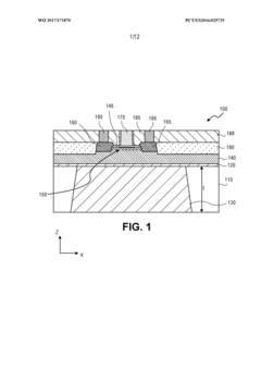
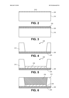
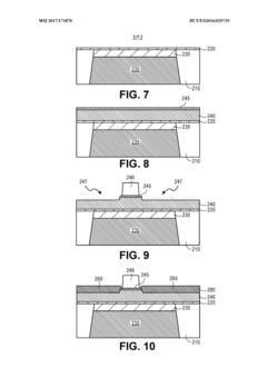
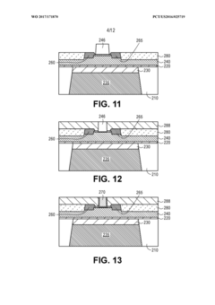
Gallium nitride transistor with underfill aluminum nitride for improved thermal and RF performance
PatentWO2017171870A1
Innovation
- Incorporating an aluminum nitride layer under the gallium nitride transistor or circuit block, utilizing a low resistivity silicon substrate, which provides both high thermal conductivity and high resistivity through the aluminum nitride's insulating properties and superior thermal conductivity compared to silicon.
Thermal Management Challenges in GaN Applications
Gallium Nitride (GaN) transistors, while offering superior performance characteristics compared to silicon-based alternatives, face significant thermal management challenges that must be addressed for reliable operation in emerging applications. The wide bandgap properties that enable GaN's high-frequency operation and power density simultaneously generate considerable heat during operation, creating thermal bottlenecks that can limit device performance and longevity.
The primary thermal challenge stems from GaN's inherent power density capabilities, which can exceed 5 W/mm² - significantly higher than silicon-based technologies. This concentrated heat generation creates localized hotspots within the device structure that must be efficiently dissipated to prevent performance degradation and premature failure. The thermal conductivity of GaN substrates, particularly in GaN-on-Si configurations, presents additional complications as the thermal boundary resistance between heterogeneous materials impedes efficient heat transfer.
Emerging applications in 5G infrastructure, electric vehicles, and data centers are pushing GaN devices to operate at higher frequencies and power levels, exacerbating these thermal challenges. For instance, 5G base stations utilizing GaN RF amplifiers must maintain stable operation under varying environmental conditions while delivering consistent high-frequency performance. Similarly, GaN-based power converters in electric vehicles must handle high-temperature automotive environments while maintaining efficiency during rapid charging cycles.
Current thermal management approaches include advanced packaging technologies such as flip-chip configurations, which minimize thermal resistance by placing the active device layer closer to heat sinks. Direct substrate cooling techniques, including microfluidic channels and two-phase cooling systems, are being explored to address the increasing thermal loads. Additionally, diamond heat spreaders, with thermal conductivity exceeding 2000 W/mK, are being integrated with GaN devices to enhance heat dissipation capabilities.
Computational fluid dynamics (CFD) modeling and finite element analysis (FEA) have become essential tools for predicting thermal behavior in complex GaN device structures. These simulation approaches enable designers to identify potential hotspots and optimize thermal management solutions before physical prototyping. Real-time temperature sensing and dynamic thermal management systems are also being developed to adaptively control device operation based on thermal conditions.
The industry is increasingly adopting system-level thermal design approaches that consider the entire thermal path from junction to ambient. This holistic perspective encompasses die-attach materials, packaging techniques, thermal interface materials, and cooling system design to create comprehensive thermal solutions for GaN applications. As GaN transistor innovation continues to accelerate, addressing these thermal management challenges will remain critical to unlocking the full potential of this transformative semiconductor technology.
Sustainability Impact of GaN Power Electronics
The adoption of Gallium Nitride (GaN) power electronics represents a significant advancement in sustainable technology development. GaN-based power devices demonstrate substantially reduced energy losses compared to traditional silicon alternatives, with efficiency improvements of 40-90% depending on the application. This translates directly into lower energy consumption across the entire electronics ecosystem, from data centers to consumer devices, contributing significantly to global energy conservation efforts.
The manufacturing process for GaN transistors requires fewer resources than silicon counterparts, with studies indicating up to 30% reduction in raw material usage. Additionally, the higher operating temperatures of GaN devices reduce or eliminate the need for complex cooling systems in many applications, further decreasing the environmental footprint of electronic systems. This aspect becomes particularly important in high-power density applications where thermal management traditionally consumes substantial resources.
GaN power electronics enable more compact and lightweight designs across various applications, reducing material usage and transportation-related carbon emissions. For instance, GaN-based power adapters can be up to 60% smaller than silicon equivalents while delivering the same or better performance. In electric vehicles, GaN power modules contribute to extended range capabilities through improved power conversion efficiency, accelerating the transition away from fossil fuel transportation.
The longer operational lifespan of GaN devices—often exceeding traditional silicon components by 3-5 years—reduces electronic waste generation. This longevity, combined with the smaller form factor, represents a significant contribution to circular economy principles in electronics manufacturing. Furthermore, GaN components contain fewer toxic materials compared to some alternative semiconductor technologies, reducing end-of-life environmental impact.
In renewable energy systems, GaN power electronics improve conversion efficiency in solar inverters and wind power systems by 2-3 percentage points, which translates to substantial additional energy capture over system lifetimes. This efficiency gain accelerates the return on investment for renewable energy installations and enhances their competitiveness against fossil fuel alternatives.
The sustainability benefits of GaN extend to emerging applications like smart grids, where high-frequency operation capabilities enable more responsive and efficient power distribution networks. These advanced grid systems can better integrate intermittent renewable energy sources, further amplifying the environmental benefits of GaN technology beyond direct device-level efficiency improvements.
Unlock deeper insights with Patsnap Eureka Quick Research — get a full tech report to explore trends and direct your research. Try now!
Generate Your Research Report Instantly with AI Agent
Supercharge your innovation with Patsnap Eureka AI Agent Platform!