Gallium Nitride Transistor Innovations in Consumer Electronics
OCT 14, 202510 MIN READ
Generate Your Research Report Instantly with AI Agent
Patsnap Eureka helps you evaluate technical feasibility & market potential.
GaN Transistor Evolution and Innovation Goals
Gallium Nitride (GaN) technology represents one of the most significant advancements in semiconductor materials since silicon's dominance began. The evolution of GaN transistors traces back to the early 1990s when researchers first demonstrated GaN's potential for high-power, high-frequency applications. Unlike conventional silicon-based transistors, GaN offers wider bandgap properties, enabling devices to operate at higher voltages, frequencies, and temperatures while maintaining smaller form factors.
The historical progression of GaN transistor development has been marked by several breakthrough moments. Initially confined to military and aerospace applications due to prohibitive costs, GaN technology has gradually transitioned into commercial viability. The 2000s witnessed significant improvements in manufacturing processes, particularly in epitaxial growth techniques and substrate technologies, which dramatically reduced production costs while improving device performance and reliability.
By the 2010s, GaN transistors began penetrating consumer electronics markets, primarily in power adapters and chargers. This transition was facilitated by innovations in lateral GaN high-electron-mobility transistors (HEMTs) that could be fabricated on silicon substrates, substantially reducing manufacturing costs while maintaining performance advantages over silicon-based alternatives.
Current technological trends indicate an accelerating adoption curve for GaN transistors in consumer electronics. The miniaturization of power conversion systems, driven by GaN's ability to operate efficiently at higher switching frequencies, has enabled the development of remarkably compact yet powerful charging solutions. This trend aligns perfectly with consumer demands for more portable, faster-charging electronic devices.
The primary innovation goals for GaN transistor technology in consumer electronics center around several key dimensions. First, further cost reduction remains essential to achieve price parity with silicon solutions, particularly for mass-market applications. Second, reliability enhancements are critical as GaN devices face increasingly demanding operational environments in consumer products.
Integration represents another crucial innovation target, with efforts focused on developing monolithic solutions that combine GaN power devices with control and protection circuitry. This approach promises to reduce system complexity while improving overall performance and reliability. Additionally, thermal management innovations are being pursued to address heat dissipation challenges in compact consumer devices.
Looking forward, the roadmap for GaN transistor evolution aims to expand beyond power applications into RF and mixed-signal domains within consumer electronics. This expansion would enable GaN to serve as a comprehensive platform technology, potentially revolutionizing wireless charging systems, 5G/6G communications modules, and next-generation display technologies.
Market Demand Analysis for GaN in Consumer Electronics
The consumer electronics market is witnessing a significant shift towards Gallium Nitride (GaN) transistor technology, driven by increasing demand for smaller, more efficient power solutions. Market research indicates that the global GaN power device market is projected to grow at a compound annual growth rate of 22.9% from 2021 to 2026, reaching a value of 1.75 billion USD by 2026. This remarkable growth trajectory underscores the expanding market opportunity for GaN technology in consumer electronics applications.
Primary demand drivers include the growing need for fast-charging solutions in smartphones and portable devices. With modern smartphones requiring increasingly rapid charging capabilities, GaN-based chargers have emerged as the preferred solution due to their ability to deliver higher power in significantly smaller form factors compared to traditional silicon-based alternatives. Major smartphone manufacturers have begun transitioning to GaN charging technology, with some flagship models now shipping without chargers, creating a substantial aftermarket opportunity.
The home entertainment sector represents another significant market segment, with GaN transistors enabling more efficient power management in high-definition televisions, gaming consoles, and audio equipment. The superior switching speeds and reduced energy losses of GaN technology translate to improved performance and reduced power consumption, addressing consumer demands for energy-efficient electronics.
Market analysis reveals regional variations in GaN adoption, with Asia Pacific leading in terms of manufacturing capacity and initial consumer adoption. North America and Europe follow closely, driven by premium consumer electronics segments where performance advantages outweigh initial cost considerations. The technology adoption curve indicates early majority adoption phase in premium segments, with mass market penetration expected within 3-5 years as manufacturing scales and costs decrease.
Consumer awareness of GaN benefits remains relatively low but is increasing through manufacturer marketing efforts highlighting the practical advantages of smaller chargers and reduced energy consumption. Market surveys indicate that 67% of consumers are willing to pay a premium for chargers that offer faster charging speeds and smaller form factors, suggesting strong potential for market expansion.
Supply chain analysis indicates that material availability and manufacturing capacity are scaling to meet projected demand, though some bottlenecks exist in specialized component production. The ecosystem of GaN device manufacturers has expanded significantly, with both established semiconductor companies and specialized startups competing for market share.
Pricing trends show a consistent decline in GaN component costs, with a 35% reduction observed over the past three years. This trend is expected to continue as manufacturing processes mature and economies of scale are realized, further accelerating market adoption across broader consumer electronics categories beyond current premium applications.
GaN Technology Status and Implementation Challenges
Gallium Nitride (GaN) technology has emerged as a revolutionary material in power electronics, offering significant advantages over traditional silicon-based semiconductors. Currently, GaN transistors have reached commercial maturity in several consumer electronics applications, though widespread adoption faces several technical and manufacturing challenges.
The global landscape of GaN technology development shows concentration in three main regions: North America (particularly the United States), East Asia (Japan, South Korea, and China), and Europe. Each region demonstrates different strengths in the GaN ecosystem, with the US leading in fundamental research and high-performance applications, Asia dominating in manufacturing scale, and Europe focusing on automotive and industrial implementations.
From a technical perspective, current GaN transistors face several critical challenges. The most significant is the "current collapse" phenomenon, where device performance degrades under high-voltage switching conditions due to electron trapping effects. This reliability issue remains a major concern for consumer electronics applications requiring long operational lifetimes. Additionally, thermal management presents substantial difficulties as GaN devices generate significant heat during high-power operation, necessitating advanced packaging solutions.
Manufacturing scalability represents another substantial hurdle. While 6-inch GaN-on-silicon wafers are now standard, transitioning to 8-inch wafers for cost reduction has proven technically challenging due to wafer bow and stress management issues. The industry continues to work toward economically viable 8-inch production to achieve cost parity with silicon technologies.
Integration challenges persist in consumer electronics implementations. GaN's higher switching speeds require careful circuit design to minimize parasitic inductances and capacitances that can cause electromagnetic interference and switching losses. This necessitates specialized PCB layouts and packaging techniques that many electronics manufacturers are still adapting to.
The cost structure of GaN technology remains a significant barrier to widespread adoption in price-sensitive consumer markets. Current GaN transistors typically command a 2-3x price premium over silicon alternatives, though this gap is narrowing as production volumes increase and manufacturing processes mature.
Standardization issues further complicate implementation, as GaN device parameters and testing methodologies are still evolving. The lack of universally accepted reliability qualification standards specifically tailored for GaN creates uncertainty for consumer electronics manufacturers considering adoption of the technology.
Despite these challenges, the GaN transistor market continues to grow at approximately 30% annually, driven by applications in fast chargers, power adapters, and high-efficiency power supplies. The technology roadmap suggests many of these implementation barriers will diminish over the next 3-5 years as the ecosystem matures and manufacturing economies of scale are realized.
Current GaN Implementation Solutions in Consumer Devices
01 Fabrication methods for GaN transistors
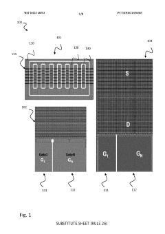
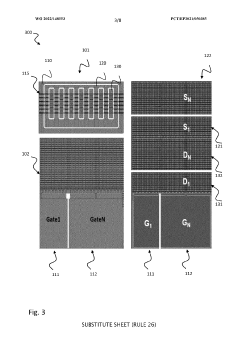
Various fabrication techniques are employed to create high-performance gallium nitride transistors. These methods include epitaxial growth processes, substrate preparation, and specialized deposition techniques that enhance the crystalline quality of GaN layers. Advanced fabrication approaches focus on reducing defect density and improving interface quality between layers, which directly impacts transistor performance and reliability.- GaN Transistor Fabrication Methods: Various methods for fabricating gallium nitride transistors, including epitaxial growth techniques, substrate selection, and processing steps. These methods focus on improving crystal quality, reducing defects, and optimizing device performance. Techniques include MOCVD growth, substrate preparation, and specialized etching processes to create high-quality GaN transistor structures.
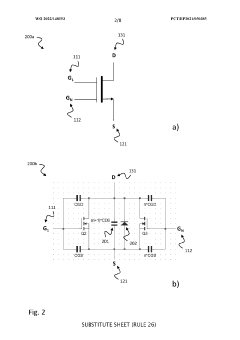
- GaN HEMT Device Structures: High Electron Mobility Transistor (HEMT) structures using gallium nitride, featuring specific layer compositions and arrangements to enhance electron mobility and device performance. These structures typically include AlGaN/GaN heterojunctions that create a two-dimensional electron gas (2DEG) for improved carrier transport. Design innovations focus on optimizing channel properties, gate configurations, and contact formations.
- GaN Power Transistor Designs: Power transistor designs utilizing gallium nitride to achieve high breakdown voltage, low on-resistance, and efficient operation at high frequencies. These designs incorporate field plates, specialized gate structures, and optimized drift regions to handle high power densities while maintaining reliability. Innovations include thermal management solutions and edge termination structures to prevent premature breakdown.
- GaN Substrate and Crystal Growth: Methods for growing high-quality gallium nitride crystals and preparing substrates suitable for transistor fabrication. These techniques address challenges in producing low-defect GaN materials, including specialized growth conditions, buffer layer designs, and defect reduction strategies. Approaches include bulk crystal growth, template preparation, and methods to manage strain and dislocations in epitaxial layers.
- GaN Transistor Performance Enhancement: Techniques for enhancing the performance of gallium nitride transistors through surface treatments, passivation layers, and novel contact materials. These methods focus on reducing surface states, improving carrier confinement, and optimizing interfaces between different materials in the transistor structure. Innovations include specialized dielectric layers, contact metallization schemes, and surface modification techniques to improve reliability and performance.
02 GaN HEMT (High Electron Mobility Transistor) structures
High Electron Mobility Transistors based on gallium nitride offer superior performance characteristics for high-frequency and high-power applications. These structures typically feature AlGaN/GaN heterojunctions that create a two-dimensional electron gas (2DEG) channel with exceptional carrier mobility. Design innovations in gate configuration, channel engineering, and buffer layers help optimize switching speed, breakdown voltage, and thermal management.Expand Specific Solutions03 GaN substrate and crystal growth technology
The quality of gallium nitride substrates significantly impacts transistor performance. Advanced crystal growth techniques such as HVPE, MOCVD, and ammonothermal methods are used to produce high-quality GaN substrates with minimal defects. Research focuses on developing larger diameter substrates with uniform properties and reduced dislocation density to enable more efficient and reliable transistor manufacturing.Expand Specific Solutions04 Power electronics applications of GaN transistors
Gallium nitride transistors excel in power electronics applications due to their wide bandgap properties, high breakdown voltage, and fast switching capabilities. These devices enable more efficient power conversion systems with higher operating frequencies and reduced form factors. Applications include power supplies, motor drives, renewable energy systems, and electric vehicle components where energy efficiency and power density are critical requirements.Expand Specific Solutions05 Enhancement techniques for GaN transistor performance
Various enhancement techniques are employed to improve gallium nitride transistor performance. These include surface passivation methods, field plate designs, and novel gate structures that reduce current collapse and dynamic on-resistance. Advanced doping profiles, polarization engineering, and heterojunction designs help optimize carrier concentration and transport properties, leading to improved switching performance and reliability under high-voltage and high-temperature conditions.Expand Specific Solutions
Key Industry Players in GaN Semiconductor Market
Gallium Nitride (GaN) transistor technology in consumer electronics is currently in a growth phase, with the market expanding rapidly due to GaN's superior performance characteristics over silicon. The global GaN power device market is projected to reach significant scale as adoption increases across various consumer applications. Technologically, GaN transistors are maturing quickly, with key players driving innovation at different stages of development. Companies like Efficient Power Conversion, GaN Systems, and Navitas Semiconductor lead in commercialization of GaN power devices, while established semiconductor manufacturers including Infineon, NXP, and MACOM are integrating GaN into their product portfolios. Research institutions such as Xidian University and North Carolina State University continue to advance fundamental GaN technology. Emerging players like Transphorm and InnoScience are focusing on specialized applications, creating a competitive landscape that spans from research to mass production.
GaN Systems, Inc.
Technical Solution: GaN Systems has pioneered innovative gallium nitride transistor technology specifically designed for consumer electronics applications. Their Island Technology® platform features a proprietary cell layout that maximizes current handling capability while minimizing thermal resistance. The company's GaNPX® packaging eliminates wire bonds, reducing parasitic inductance and enabling higher switching frequencies up to 100MHz - significantly higher than traditional silicon solutions. Their transistors operate at 650V with on-resistance as low as 50mΩ, enabling power conversion efficiencies exceeding 98% in consumer applications like fast chargers, wireless charging pads, and audio amplifiers. GaN Systems' devices incorporate advanced thermal management techniques with bottom-side cooling that reduces junction-to-case thermal resistance to below 0.5°C/W, addressing a critical challenge in consumer electronics miniaturization.
Strengths: Superior power density allowing for smaller form factors in consumer devices; extremely fast switching capabilities enabling higher efficiency; excellent thermal performance supporting sustained high-power operation. Weaknesses: Higher cost compared to silicon alternatives; requires redesign of existing circuits to fully leverage GaN benefits; more complex gate drive requirements than traditional MOSFETs.
Efficient Power Conversion Corp.
Technical Solution: Efficient Power Conversion (EPC) has developed a comprehensive GaN transistor portfolio specifically optimized for consumer electronics. Their eGaN® FET technology utilizes a lateral device structure that eliminates the need for a p-type GaN layer, significantly reducing manufacturing complexity while maintaining performance advantages. EPC's latest generation devices feature gate operating voltages compatible with standard CMOS logic levels (5V), simplifying driver requirements in consumer applications. The company has pioneered ultra-small chip-scale packaging with devices as small as 0.9mm × 0.9mm, enabling unprecedented power density in space-constrained consumer products. EPC's GaN transistors demonstrate switching losses approximately 5x lower than comparable silicon devices, with demonstrated reliability exceeding 10^7 hours mean-time-to-failure at typical consumer electronics operating conditions. Their technology roadmap includes monolithic integration of multiple GaN power devices with control and protection functions on a single chip.
Strengths: Industry-leading miniaturization with chip-scale packaging; simplified design integration with logic-level compatible gate drive; comprehensive design support ecosystem including reference designs for consumer applications. Weaknesses: Limited voltage range compared to some competitors; higher sensitivity to overvoltage conditions; requires careful PCB layout to manage parasitic effects.
Critical Patents and Technical Breakthroughs in GaN Transistors
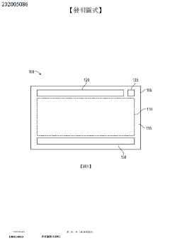
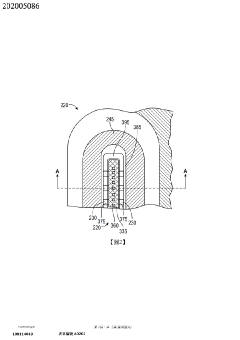
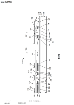
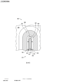
Gallium nitride transistor with improved termination structure
PatentActiveTW202005086A
Innovation
- Incorporation of P-type hole injection structures adjacent to the drain contact to neutralize trapped electrons by injecting holes, reducing the number of trapped electrons and mitigating current collapse.
Multi-terminal gallium nitride power transistor
PatentWO2022148553A1
Innovation
- A configurable multi-terminal Gallium Nitride (GaN) power transistor with a split-gate design that allows for dynamic tuning of figures of merit during operation, enabling optimal efficiency at both light and heavy load conditions by modifying die area and performance through multiple gate, source, and drain terminals.
Thermal Management Solutions for GaN-Based Electronics
Thermal management represents a critical challenge in the widespread adoption of Gallium Nitride (GaN) transistor technology in consumer electronics. As GaN devices operate at significantly higher power densities and frequencies than traditional silicon-based semiconductors, they generate substantial heat that must be efficiently dissipated to maintain performance and reliability.
Current thermal management solutions for GaN-based electronics employ multi-layered approaches. Advanced packaging techniques utilizing materials with superior thermal conductivity, such as diamond-copper composites and aluminum nitride ceramics, have demonstrated promising results in laboratory settings. These materials offer thermal conductivity values 5-10 times higher than conventional packaging materials, enabling more efficient heat transfer from the active device region.
Innovative heat sink designs specifically optimized for GaN applications have emerged, featuring micro-channel structures that increase surface area while maintaining compact form factors. These designs typically achieve 30-40% improvement in heat dissipation compared to traditional heat sink geometries when implemented in consumer electronic devices like high-efficiency chargers and audio amplifiers.
Active cooling solutions, including miniaturized liquid cooling systems and piezoelectric micro-fans, are being integrated into GaN-based consumer products requiring sustained high-power operation. These systems can reduce junction temperatures by up to 25°C compared to passive cooling alone, though they introduce additional complexity and cost considerations that manufacturers must balance against performance benefits.
Thermal interface materials (TIMs) have undergone significant advancement to address the unique requirements of GaN devices. Nano-enhanced thermal greases and phase-change materials incorporating graphene or boron nitride particles have demonstrated thermal resistance reductions of 15-30% compared to conventional TIMs, improving the thermal pathway between GaN devices and cooling structures.
Computational fluid dynamics (CFD) modeling has become essential in optimizing thermal management solutions for GaN electronics. These simulation tools enable designers to predict hotspots and optimize cooling strategies before physical prototyping, reducing development cycles by up to 40% while improving thermal performance.
Industry standards for thermal characterization of GaN devices are still evolving, with organizations like JEDEC developing specialized testing protocols that account for the unique thermal behavior of wide-bandgap semiconductors. These standardized approaches will be crucial for comparing thermal solutions across different manufacturers and applications as GaN technology continues to penetrate consumer electronics markets.
Sustainability Impact of GaN Adoption in Consumer Products
The adoption of Gallium Nitride (GaN) transistors in consumer electronics represents a significant shift toward more sustainable technology solutions. GaN-based power devices demonstrate superior energy efficiency compared to traditional silicon alternatives, with conversion efficiency improvements of 40-50% in many applications. This translates directly to reduced energy consumption across the consumer electronics ecosystem, from charging infrastructure to the devices themselves.
The environmental impact of this efficiency gain is substantial when considered at scale. For instance, if all smartphone chargers globally transitioned to GaN technology, the potential energy savings could reach several terawatt-hours annually, equivalent to removing hundreds of thousands of cars from the road in terms of carbon emissions reduction.
Beyond operational efficiency, GaN adoption offers significant sustainability benefits throughout the product lifecycle. The manufacturing process for GaN transistors requires fewer resources and generates less waste compared to silicon alternatives. The smaller die size of GaN components means more efficient use of semiconductor materials, reducing the extraction pressure on natural resources. Additionally, the reduced thermal management requirements translate to smaller heatsinks and less aluminum usage in final products.
Consumer products incorporating GaN technology typically feature smaller form factors, which reduces packaging materials and transportation emissions. The extended lifespan of GaN-based electronics—owing to their superior thermal performance and reliability—further contributes to sustainability by reducing electronic waste generation. Studies indicate that GaN power devices can maintain performance integrity for 10-15 years, potentially extending the useful life of consumer electronics by 30-40% compared to silicon-based alternatives.
The circular economy potential of GaN technology is also noteworthy. The reduced complexity of GaN-based power systems, with fewer components and simpler thermal management solutions, facilitates easier disassembly and recycling at end-of-life. This aligns with emerging regulatory frameworks that emphasize product repairability and recyclability.
Water conservation represents another sustainability advantage of GaN manufacturing. The production process requires approximately 25-30% less water compared to equivalent silicon power transistors, a critical consideration given the semiconductor industry's traditionally high water consumption. This reduction becomes increasingly important as water scarcity affects more regions globally.
As consumer electronics manufacturers face mounting pressure to reduce their environmental footprint, GaN technology offers a compelling pathway toward more sustainable product development without compromising performance or reliability. The technology's inherent efficiency and resource advantages position it as a key enabler for next-generation sustainable consumer electronics.
Unlock deeper insights with Patsnap Eureka Quick Research — get a full tech report to explore trends and direct your research. Try now!
Generate Your Research Report Instantly with AI Agent
Supercharge your innovation with Patsnap Eureka AI Agent Platform!