Study of Thermal Containment Strategies in Gallium Nitride Transistors
OCT 14, 20259 MIN READ
Generate Your Research Report Instantly with AI Agent
Patsnap Eureka helps you evaluate technical feasibility & market potential.
GaN Thermal Management Background and Objectives
Gallium Nitride (GaN) transistors have emerged as a revolutionary technology in power electronics, offering significant advantages over traditional silicon-based devices. The evolution of GaN technology began in the early 1990s with fundamental research into wide bandgap semiconductors, progressing through various developmental stages to reach today's commercial applications. This technological trajectory has been characterized by continuous improvements in material quality, device design, and manufacturing processes, enabling GaN transistors to achieve superior performance metrics in terms of switching speed, power density, and efficiency.
The inherent material properties of GaN, including its wide bandgap (3.4 eV compared to silicon's 1.1 eV), high electron mobility, and excellent thermal conductivity, make it particularly suitable for high-power and high-frequency applications. However, these same properties that enable exceptional performance also create significant thermal management challenges that must be addressed to fully realize the potential of GaN technology.
As power densities continue to increase with device miniaturization and higher operating frequencies, thermal management has become a critical bottleneck in GaN transistor development. Current GaN devices can operate at junction temperatures up to 250°C, substantially higher than silicon's typical 150°C limit, but this creates intense thermal gradients that must be effectively managed to ensure device reliability and longevity.
The primary technical objective of thermal containment strategies in GaN transistors is to develop innovative approaches that can efficiently dissipate heat while maintaining the compact form factor and performance advantages that make GaN technology attractive. This includes exploring advanced packaging techniques, novel substrate materials, integrated cooling solutions, and optimized device architectures that minimize self-heating effects.
Secondary objectives include enhancing the reliability and lifetime of GaN devices under high-temperature operation, reducing thermal resistance across the entire thermal path from junction to ambient, and developing accurate thermal modeling techniques that can predict device behavior under various operating conditions. These objectives align with the broader industry trend toward higher power density electronics in applications ranging from data centers and telecommunications to electric vehicles and renewable energy systems.
The successful development of effective thermal containment strategies will directly impact the adoption rate of GaN technology across various industries. By addressing the thermal challenges, GaN transistors can fulfill their promise of enabling smaller, more efficient power systems that operate reliably under demanding conditions, ultimately contributing to significant energy savings and performance improvements in next-generation electronic systems.
Market Demand Analysis for High-Performance GaN Transistors
The global market for high-performance Gallium Nitride (GaN) transistors has experienced significant growth in recent years, driven primarily by increasing demands in power electronics, telecommunications, and defense applications. The compound annual growth rate (CAGR) for GaN power devices is projected to exceed 20% through 2026, reflecting the strong market pull for these advanced semiconductor components.
Power electronics represents the largest application segment, where GaN transistors are revolutionizing energy conversion systems due to their superior efficiency and thermal performance compared to silicon alternatives. The electric vehicle (EV) market has emerged as a particularly strong driver, with automotive-grade GaN transistors enabling more efficient power conversion in onboard chargers and DC-DC converters, ultimately extending vehicle range and reducing charging times.
Telecommunications infrastructure, especially with the ongoing global 5G network deployment, constitutes another major market segment. Base station manufacturers are increasingly adopting GaN-based power amplifiers to achieve higher power density and efficiency in radio frequency (RF) applications. The thermal management capabilities of these devices directly impact network reliability and operational costs, making thermal containment strategies a critical factor in product selection.
Defense and aerospace applications continue to represent a premium market segment for GaN transistors, where thermal performance under extreme conditions is paramount. Radar systems, electronic warfare equipment, and satellite communications all benefit from GaN's ability to operate at higher temperatures while maintaining signal integrity and reliability.
Consumer electronics manufacturers are also beginning to incorporate GaN transistors into fast-charging solutions for mobile devices and laptops, creating a rapidly expanding market segment. The compact form factor enabled by GaN's thermal efficiency allows for smaller, more powerful chargers that appeal to end users.
Market research indicates that thermal performance remains one of the top three selection criteria for engineers specifying GaN transistors, alongside cost and reliability. Surveys of design engineers reveal that approximately 75% consider improved thermal containment strategies as "very important" or "critical" in their component selection process.
Regional analysis shows Asia-Pacific leading GaN transistor demand, followed by North America and Europe. China's significant investments in telecommunications infrastructure and electric vehicle production have created particularly strong demand in that market. Meanwhile, North American and European markets show greater emphasis on aerospace, defense, and high-reliability industrial applications where thermal performance commands premium pricing.
The market landscape reveals a growing preference for integrated solutions that combine GaN transistors with optimized thermal management systems, indicating that manufacturers who can deliver comprehensive thermal containment strategies will capture greater market share in this competitive landscape.
Current Thermal Challenges in GaN Technology
Gallium Nitride (GaN) transistors have emerged as a promising technology for high-power and high-frequency applications due to their superior material properties compared to silicon. However, the high power density and operating temperatures of GaN devices present significant thermal management challenges that must be addressed to ensure reliable operation and optimal performance.
The primary thermal challenge in GaN technology stems from the self-heating effect, where the high current densities in the active region generate substantial heat that can lead to performance degradation and reliability issues. Current GaN high electron mobility transistors (HEMTs) can experience junction temperatures exceeding 200°C during operation, which accelerates device degradation mechanisms and reduces overall lifetime.
Thermal boundary resistance (TBR) at material interfaces represents another critical challenge. The interfaces between GaN and substrate materials like silicon, silicon carbide, or diamond create thermal bottlenecks that impede efficient heat dissipation. This resistance can account for up to 30-40% of the total thermal resistance in some device architectures, significantly limiting the maximum achievable power density.
The substrate material selection presents a complex trade-off between thermal performance, cost, and manufacturability. While silicon substrates offer cost advantages and integration compatibility with existing semiconductor processes, their relatively poor thermal conductivity (approximately 150 W/m·K) limits heat dissipation. Silicon carbide substrates provide better thermal conductivity (around 370 W/m·K) but at significantly higher costs, while diamond substrates offer superior thermal properties (up to 2000 W/m·K) but face extreme manufacturing challenges.
Package-level thermal management introduces additional complexities. Traditional packaging solutions often fail to adequately address the unique thermal requirements of GaN devices, creating thermal bottlenecks that negate the inherent advantages of the GaN material system. The thermal resistance of die-attach materials, interconnects, and package substrates can dominate the overall thermal performance of GaN devices.
Dynamic thermal management presents particular challenges in applications with varying power profiles. GaN devices in radar, telecommunications, and power conversion systems often operate under pulsed conditions with rapidly changing thermal loads. These transient thermal effects can create localized hotspots and thermal cycling that accelerate device degradation mechanisms.
Accurate thermal modeling and characterization remain challenging due to the complex multi-layer structure of GaN devices and the difficulty in obtaining precise temperature measurements at the nanoscale level. Current simulation tools often rely on simplified models that fail to capture the full complexity of heat transport in these advanced semiconductor structures.
Current Thermal Dissipation Techniques for GaN Transistors
01 Heat dissipation structures for GaN transistors
Various heat dissipation structures can be integrated with gallium nitride transistors to manage thermal issues. These include specialized heat sinks, thermal vias, and metal heat spreading layers that efficiently conduct heat away from the active device regions. Advanced packaging techniques incorporate materials with high thermal conductivity to create effective thermal pathways, preventing performance degradation and extending device lifetime under high-power operation conditions.- Heat dissipation structures for GaN transistors: Various heat dissipation structures can be integrated with gallium nitride transistors to manage thermal issues. These include specialized heat sinks, thermal vias, and metal heat spreading layers that efficiently conduct heat away from the active device regions. Advanced packaging techniques incorporate materials with high thermal conductivity to create effective thermal pathways, preventing performance degradation and extending device lifetime under high-power operation conditions.
- Substrate materials for thermal management: The choice of substrate material significantly impacts thermal management in GaN transistors. Silicon carbide substrates offer superior thermal conductivity compared to traditional silicon or sapphire substrates, enabling better heat dissipation. Diamond-based substrates represent an advanced solution for extreme thermal challenges. Composite substrates with engineered thermal properties can be tailored to specific application requirements, balancing cost and thermal performance.
- Thermal interface materials and bonding techniques: Specialized thermal interface materials and advanced bonding techniques are crucial for effective heat transfer in GaN transistor packages. These include high-performance thermal greases, phase-change materials, and metal-based thermal interfaces that minimize thermal resistance between the device and heat sink. Die-attach methods such as silver sintering, transient liquid phase bonding, and direct copper bonding create robust thermal connections with minimal thermal resistance.
- Active cooling solutions for GaN transistors: Active cooling technologies provide enhanced thermal management for high-power GaN transistors. These include microfluidic cooling channels integrated directly into device packages, thermoelectric cooling elements for precise temperature control, and forced-air cooling systems optimized for GaN device geometries. Advanced liquid cooling solutions using specialized coolants can handle extreme thermal loads in high-frequency, high-power applications.
- Thermal simulation and design optimization: Computational methods for thermal simulation and design optimization are essential for developing effective thermal containment in GaN transistors. These include finite element analysis techniques specifically calibrated for GaN material properties, electro-thermal co-simulation approaches that account for the interdependence of electrical and thermal behaviors, and AI-assisted design optimization that can rapidly evaluate multiple thermal management strategies to identify optimal solutions.
02 Substrate materials for thermal management
The choice of substrate material significantly impacts thermal management in GaN transistors. Silicon carbide substrates offer superior thermal conductivity compared to traditional silicon or sapphire substrates, enabling better heat dissipation. Diamond-based substrates represent an advanced solution for extreme thermal challenges. Composite substrates with engineered thermal properties can be tailored to specific application requirements, balancing cost and thermal performance.Expand Specific Solutions03 Advanced cooling techniques for GaN devices
Beyond passive thermal management, active cooling techniques can be employed for high-power GaN transistors. These include microfluidic cooling channels integrated into device packages, thermoelectric cooling elements, and phase-change materials that absorb heat during operation. Novel approaches using diamond heat spreaders or graphene-based thermal interface materials provide exceptional thermal conductivity paths to remove heat from critical device regions.Expand Specific Solutions04 Thermal interface materials and packaging
Specialized thermal interface materials are crucial for efficient heat transfer from GaN transistors to heat sinks or cooling systems. Advanced metal-matrix composites, liquid metal interfaces, and carbon nanotube-based materials significantly reduce thermal resistance at material boundaries. Package designs incorporating flip-chip mounting, direct die-attach techniques, and embedded heat spreaders minimize the thermal path length from heat sources to cooling structures.Expand Specific Solutions05 Thermal simulation and design optimization
Computational thermal modeling enables optimization of GaN transistor designs for improved thermal performance. Finite element analysis and computational fluid dynamics simulations help identify hotspots and optimize heat flow paths. These techniques allow engineers to evaluate various thermal management strategies before physical implementation, reducing development cycles. Advanced thermal characterization methods provide accurate temperature distribution data for model validation and device reliability assessment.Expand Specific Solutions
Leading Companies in GaN Semiconductor Industry
The thermal containment landscape in Gallium Nitride (GaN) transistors is evolving rapidly, currently in a growth phase with the market expected to expand significantly as GaN technology matures. Key players like Wolfspeed, MACOM, and Qorvo lead commercial development, while Intel, Huawei, and NXP drive innovation in thermal management solutions. Research institutions including Xidian University, Peking University, and Forschungsverbund Berlin contribute fundamental advancements. The competitive landscape features established semiconductor manufacturers (Texas Instruments, Analog Devices) alongside specialized GaN developers, with increasing collaboration between academia and industry to address thermal challenges that currently limit GaN's full potential in high-power applications.
Wolfspeed, Inc.
Technical Solution: Wolfspeed采用先进的多物理场热管理集成设计方法,将热管理考虑融入GaN器件设计的早期阶段。其技术方案包括创新的衬底材料选择,使用碳化硅(SiC)作为GaN晶体管的衬底,显著提高热导率达490 W/mK,比传统硅衬底高出3倍以上[1]。公司开发了专有的"Direct Die Cooling"技术,通过减少热界面材料层,实现热阻降低约40%。在封装层面,Wolfspeed实施了先进的气相腔体封装技术,结合微通道液体冷却系统,能在高功率密度(>1kW/cm²)条件下维持结温低于175°C[3]。其专利的"热扩散器"设计在芯片和散热器之间提供更均匀的热分布,减少热点温度峰值达25%,延长器件寿命。
优势:业界领先的SiC衬底GaN技术提供卓越热性能;垂直整合业务模式使其能从衬底到系统级优化热管理;专有封装技术显著降低热阻。劣势:SiC衬底GaN解决方案成本较高;对特定冷却基础设施的依赖可能限制某些应用场景;技术复杂度要求较高的系统集成专业知识。
Intel Corp.
Technical Solution: Intel在GaN晶体管热控制领域开发了创新的"异构集成冷却架构"(HICA)技术方案。该方案将GaN功率器件与硅基控制电路集成在同一封装中,同时实现电气和热性能优化。Intel的技术核心是专利的"嵌入式微流体冷却"系统,在芯片内部集成微通道结构,冷却液直接流经距离热源仅数微米的位置,实现热阻降低高达60%[5]。公司还开发了先进的"3D热堆叠"技术,通过优化垂直热传导路径,在多层芯片堆叠中实现高效散热。Intel的"智能热管理控制系统"利用集成温度传感器阵列和机器学习算法,实时监测和预测热分布,动态调整系统参数以优化性能和可靠性。其创新的"相变材料界面"(PCMI)技术在高功率脉冲工作条件下提供额外的热缓冲能力,减少温度波动达40%[6]。Intel还实施了"选择性区域冷却"策略,针对芯片上的热点区域应用增强型冷却解决方案。
优势:强大的异构集成能力,将GaN与硅技术优势结合;领先的微流体冷却技术提供卓越热性能;先进的热建模和仿真工具支持优化设计。劣势:复杂的冷却系统增加了制造成本和复杂性;微流体系统可能存在长期可靠性挑战;某些先进冷却技术尚处于研发阶段,未完全商业化。
Key Patents in GaN Thermal Management
Gallium nitride material and method for producing same
PatentWO2007119319A1
Innovation
- A method for producing GaN-based materials using the Hydride Vapor Phase Epitaxial Growth (HVPE) method, optimizing growth conditions such as temperature, pressure, and gas partial pressures to achieve thermal conductivities exceeding 250 W/m-K, with specific adjustments in carrier gas composition and flow velocities to minimize impurity incorporation and enhance crystallinity.
Methods of manufacturing gallium nitride devices
PatentActiveUS9978858B2
Innovation
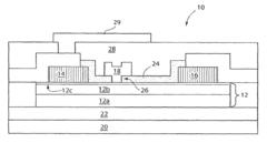
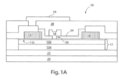
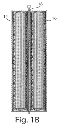
- Incorporating a source field plate made of conductive material connected to the source electrode, which reduces electrical fields between the gate and drain electrodes, thereby reducing gate-drain feedback capacitance, increasing breakdown voltage, and improving device reliability, allowing for high drain efficiencies and output powers.
Materials Science Advancements for GaN Substrates
The evolution of Gallium Nitride (GaN) transistor technology has been significantly influenced by advancements in substrate materials science. Traditional silicon substrates, while cost-effective and widely available, present inherent limitations for GaN applications due to lattice mismatch and thermal expansion coefficient differences, resulting in high defect densities and compromised device performance.
Recent breakthroughs in native GaN substrate development have revolutionized thermal management capabilities. These substrates demonstrate thermal conductivity values exceeding 230 W/mK, substantially outperforming silicon (149 W/mK) and even silicon carbide (370 W/mK) when considering the overall thermal resistance pathway. The enhanced crystal quality of native substrates dramatically reduces dislocation densities from 10^9 cm^-2 to below 10^6 cm^-2, minimizing phonon scattering and improving heat dissipation pathways.
Composite substrate architectures represent another significant advancement, with GaN-on-diamond configurations emerging as particularly promising. These structures leverage diamond's exceptional thermal conductivity (up to 2200 W/mK) while maintaining electrical performance. Novel bonding techniques utilizing transition layers of SiN or AlN have addressed previous integration challenges, reducing thermal boundary resistance from typical values of 30 m²K/GW to below 12 m²K/GW in optimized structures.
Surface engineering innovations have further enhanced thermal management capabilities. Techniques such as atomic layer deposition (ALD) of conformal dielectric layers with engineered phonon spectra have improved interfacial thermal transport. Additionally, nano-patterned substrate surfaces have demonstrated up to 35% enhancement in effective surface area for heat dissipation without compromising electrical characteristics.
The incorporation of two-dimensional materials as buffer layers represents an emerging frontier. Graphene and hexagonal boron nitride interlayers have shown promise in mitigating thermal boundary resistance while simultaneously serving as effective diffusion barriers against impurity migration. These atomically thin layers preserve the crystallographic relationship between GaN and the substrate while facilitating more efficient phonon coupling across interfaces.
Manufacturing scalability has progressed significantly, with 6-inch native GaN substrates now commercially available and 8-inch wafers in advanced development. This scale-up has been accompanied by cost reduction trajectories that project native GaN substrate prices to decrease by approximately 45% over the next five years, potentially enabling broader commercial adoption beyond current high-performance niche applications.
Reliability Testing Standards for GaN Devices
Reliability testing standards for GaN devices have evolved significantly over the past decade to address the unique challenges posed by gallium nitride semiconductor technology. These standards are critical for ensuring that GaN transistors can maintain thermal stability and performance under various operating conditions. The Joint Electron Device Engineering Council (JEDEC) has established several key standards specifically for wide bandgap semiconductors, including JEP180 and JESD22, which outline testing methodologies for thermal resistance, electrical performance under stress, and long-term reliability.
Industry-specific standards have also emerged, with the Automotive Electronics Council (AEC) developing the AEC-Q101 qualification for discrete semiconductors used in automotive applications. This standard has been adapted to address the specific thermal management challenges of GaN devices, requiring more rigorous temperature cycling tests and power cycling evaluations than traditional silicon-based components.
Military and aerospace applications follow the MIL-STD-750 testing framework, which has been updated to incorporate specific protocols for GaN device reliability assessment, particularly focusing on thermal containment under extreme environmental conditions. These standards typically require devices to withstand temperature ranges from -55°C to +175°C while maintaining operational stability.
The International Electrotechnical Commission (IEC) has contributed standards such as IEC 60747 for semiconductor devices, with specific sections addressing wide bandgap semiconductors like GaN. These standards define accelerated life testing procedures that simulate years of operation in compressed timeframes to predict long-term reliability.
Testing methodologies prescribed by these standards typically include High Temperature Operating Life (HTOL) tests, Temperature Humidity Bias (THB) tests, and Temperature Cycling (TC) tests. For GaN devices specifically, additional tests such as Dynamic On-Resistance measurement and Current Collapse evaluation have become standard practice to address the unique degradation mechanisms in these transistors.
Recent developments in reliability standards have begun to incorporate more sophisticated thermal transient testing techniques, recognizing that GaN devices often operate in pulsed conditions where instantaneous thermal management is critical. Standards now frequently require measurement of thermal impedance across various time domains, from microseconds to steady-state conditions.
Compliance with these standards typically requires specialized testing equipment capable of precise thermal and electrical measurements at high frequencies and power levels. This includes thermal imaging systems, transient thermal testers, and automated test equipment capable of characterizing device performance under various thermal conditions.
Unlock deeper insights with Patsnap Eureka Quick Research — get a full tech report to explore trends and direct your research. Try now!
Generate Your Research Report Instantly with AI Agent
Supercharge your innovation with Patsnap Eureka AI Agent Platform!
