Gallium Nitride Transistors: Exploring Thermal Conductivity Limits
OCT 14, 20259 MIN READ
Generate Your Research Report Instantly with AI Agent
Patsnap Eureka helps you evaluate technical feasibility & market potential.
GaN Transistor Evolution and Performance Targets
Gallium Nitride (GaN) transistor technology has undergone significant evolution since its inception in the early 1990s. The journey began with rudimentary GaN-based high electron mobility transistors (HEMTs) that demonstrated promising theoretical capabilities but faced substantial manufacturing challenges. By the early 2000s, researchers had overcome initial obstacles related to substrate quality and epitaxial growth techniques, enabling the first commercial GaN transistors for RF applications.
The evolution accelerated between 2010-2015 when enhanced fabrication processes allowed for reduced gate lengths below 100nm, dramatically improving frequency response and power handling capabilities. This period marked a critical transition from primarily research-focused development to commercial viability in specialized markets such as military radar and telecommunications infrastructure.
Recent years have witnessed a paradigm shift toward addressing thermal management challenges, as power density capabilities have increased exponentially. The thermal conductivity limitations have become the primary bottleneck in further performance enhancement, with current GaN devices operating at power densities exceeding 40W/mm² - approximately ten times higher than traditional silicon-based technologies.
Performance targets for next-generation GaN transistors focus on several key parameters. First, breakdown voltage targets have been established at >1200V for power electronics applications, representing a 50% improvement over current commercial offerings. Second, on-resistance specifications aim for <0.5mΩ·cm², which would enable unprecedented efficiency in power conversion systems.
Thermal management targets have become increasingly stringent, with industry roadmaps indicating the need for solutions capable of dissipating heat fluxes exceeding 1000W/cm² while maintaining junction temperatures below 175°C. This represents a significant challenge given the current thermal conductivity limitations of GaN substrates (approximately 130W/m·K compared to 1500W/m·K for diamond).
Switching frequency capabilities are expected to reach beyond 100MHz for hard-switching applications, enabling dramatic reductions in passive component sizes and overall system footprints. This performance target is particularly relevant for emerging applications in electric vehicles and renewable energy systems where space and weight constraints are significant considerations.
Reliability metrics have also evolved, with current targets specifying less than 10 FIT (failures in time) rates under maximum rated conditions for 15+ years of operation. This represents an order of magnitude improvement over early GaN devices and addresses a critical adoption barrier in conservative industries such as automotive and industrial power systems.
The trajectory of GaN transistor evolution clearly points toward a future where thermal conductivity limitations must be overcome to unlock the full theoretical performance potential of this wide-bandgap semiconductor technology. Current research focuses on novel substrate materials, advanced packaging techniques, and innovative device architectures designed specifically to address these thermal constraints.
Market Analysis for High-Power GaN Applications
The global market for high-power GaN applications is experiencing robust growth, driven by increasing demand for efficient power electronics across multiple sectors. The market size for GaN power devices reached approximately $223 million in 2022 and is projected to grow at a compound annual growth rate (CAGR) of 33.4% through 2028, potentially reaching over $1.2 billion by the end of the forecast period.
Key application segments demonstrating significant demand include electric vehicles (EVs), renewable energy systems, industrial motor drives, and telecommunications infrastructure. The EV segment represents the fastest-growing market, with GaN transistors increasingly adopted in onboard chargers and DC-DC converters due to their superior thermal performance compared to silicon alternatives. This segment alone is expected to grow at a CAGR of 38% through 2028.
The renewable energy sector constitutes another major market driver, with solar inverters and wind power converters benefiting from GaN's ability to operate efficiently at high temperatures. Market penetration in this sector has increased from 5% in 2020 to approximately 12% in 2023, with projections suggesting 25% market share by 2027.
Regional analysis reveals Asia-Pacific as the dominant market, accounting for 42% of global GaN power device consumption, followed by North America (31%) and Europe (22%). China and Japan lead manufacturing capacity, while significant R&D investments are concentrated in the United States and Germany.
Market barriers include relatively high production costs compared to silicon alternatives, with GaN solutions typically commanding a 2.5-3x price premium. However, this gap is narrowing as manufacturing scales up, with price premiums expected to decrease to 1.5x by 2026 according to industry forecasts.
Customer adoption patterns indicate a two-tiered market: high-end applications where thermal performance is critical are rapidly embracing GaN technology despite cost premiums, while mass-market adoption awaits further price reductions. Survey data from power electronics engineers shows 67% recognize GaN's thermal advantages, but only 28% have implemented the technology in production designs.
The competitive landscape features both specialized GaN manufacturers like GaN Systems and Navitas Semiconductor, alongside traditional semiconductor giants including Infineon, Texas Instruments, and STMicroelectronics who have developed GaN product lines. Market concentration remains moderate with the top five players controlling approximately 63% of market share.
Thermal Conductivity Challenges in GaN Technology
Gallium Nitride (GaN) technology has emerged as a promising alternative to silicon-based semiconductors due to its superior electrical properties. However, thermal management remains one of the most significant challenges hindering the full potential of GaN transistors. The thermal conductivity of GaN, while theoretically high at approximately 230 W/mK for bulk single crystals, is substantially reduced in practical device implementations due to various material and structural factors.
The primary thermal conductivity limitation stems from the substrate materials used for GaN epitaxial growth. Silicon carbide (SiC) substrates offer relatively good thermal conductivity (370-490 W/mK), but their high cost limits widespread adoption. More economical silicon substrates suffer from poor thermal conductivity (150 W/mK) and create thermal boundary resistance at the GaN-Si interface due to lattice mismatch and interfacial defects.
Interface quality between GaN and substrate materials creates significant thermal bottlenecks. The transition layers necessary to accommodate lattice mismatches between GaN and substrates like silicon or sapphire introduce additional thermal resistance. These buffer layers, often composed of AlN or AlGaN, typically exhibit lower thermal conductivity than bulk GaN, creating heat flow constrictions that impede efficient thermal dissipation.
Device geometry and scaling present another dimension to thermal challenges. As GaN transistors are miniaturized for higher integration density, the power density increases dramatically, creating localized hotspots. The three-dimensional heat spreading becomes increasingly constrained in smaller devices, exacerbating thermal management issues. Current density concentrations near the gate edge in high-electron-mobility transistors (HEMTs) create severe thermal gradients that accelerate device degradation.
Material defects inherent to GaN epitaxial growth significantly impact thermal performance. Dislocations, point defects, and grain boundaries act as phonon scattering centers, reducing the effective thermal conductivity by up to 50% compared to theoretical values. The density of these defects varies with growth techniques and substrate choices, creating variability in thermal performance across different manufacturing processes.
The temperature dependence of GaN thermal conductivity presents additional complications. Unlike silicon, whose thermal conductivity decreases gradually with temperature, GaN exhibits a more pronounced reduction—approximately following a T^-1.4 relationship. This means that as GaN devices heat up during operation, their ability to conduct heat away diminishes more rapidly, potentially leading to thermal runaway conditions under high-power operation.
Packaging solutions for GaN devices must address these unique thermal challenges. Traditional packaging approaches optimized for silicon devices often prove inadequate for the higher power densities and thermal gradients present in GaN technology. Advanced thermal interface materials, direct substrate cooling, and novel heat spreading techniques are being explored to overcome these limitations.
Current Thermal Management Solutions for GaN Transistors
01 Substrate materials for thermal management
The choice of substrate material significantly impacts the thermal conductivity of gallium nitride transistors. Materials such as silicon carbide (SiC), diamond, and aluminum nitride offer superior thermal conductivity compared to traditional silicon substrates. These materials facilitate efficient heat dissipation from the active GaN layer, allowing the transistors to operate at higher power densities without thermal degradation. The thermal interface between the GaN layer and substrate is critical for maximizing heat transfer and maintaining optimal device performance.- Substrate materials for thermal management: The choice of substrate material significantly impacts the thermal conductivity of gallium nitride transistors. Materials like silicon carbide (SiC), diamond, and sapphire are used as substrates due to their high thermal conductivity properties. These substrates help in efficient heat dissipation from the active GaN layer, reducing thermal resistance and improving device performance under high-power operations. The thermal interface between the GaN layer and substrate is critical for overall heat transfer efficiency.
- Heat dissipation structures and packaging techniques: Advanced packaging techniques and heat dissipation structures are essential for managing thermal conductivity in GaN transistors. These include flip-chip bonding, through-substrate vias, integrated heat spreaders, and thermal interface materials. Such structures create efficient thermal pathways from the active device region to heat sinks or cooling systems. Optimized package designs can significantly reduce junction temperatures and thermal resistance, allowing GaN transistors to operate at higher power densities without performance degradation.
- Buffer layer engineering for thermal conductivity: Buffer layers between the GaN active region and substrate play a crucial role in thermal management. Engineered buffer layers with optimized composition, thickness, and growth conditions can reduce thermal boundary resistance and improve heat flow. Techniques such as graded buffer layers, superlattice structures, and nucleation layers help mitigate lattice mismatch while enhancing thermal conductivity. The quality of these intermediate layers significantly affects the overall thermal performance of GaN transistor devices.
- Novel growth techniques for high thermal conductivity GaN: Advanced epitaxial growth techniques are developed to enhance the thermal conductivity of GaN layers. Methods such as hydride vapor phase epitaxy (HVPE), metal-organic chemical vapor deposition (MOCVD), and molecular beam epitaxy (MBE) with optimized parameters can produce GaN crystals with fewer defects and higher thermal conductivity. Techniques for reducing dislocation density and controlling crystal orientation also contribute to improved thermal properties. These growth methods focus on creating high-quality GaN with minimal impurities that can impede heat flow.
- Integration of high thermal conductivity materials: Incorporating high thermal conductivity materials within GaN transistor structures enhances heat dissipation. This includes the integration of diamond heat spreaders, graphene layers, metal heat sinks, and advanced thermal interface materials. Techniques such as wafer bonding, direct growth on high thermal conductivity substrates, and composite material structures are employed. These approaches create efficient thermal pathways from the heat-generating regions to the external environment, significantly improving the thermal management of high-power GaN transistors.
02 Heat dissipation structures and packaging
Advanced packaging techniques and heat dissipation structures are essential for managing thermal conductivity in GaN transistors. These include flip-chip bonding, thermal vias, heat spreaders, and specialized heat sinks designed specifically for GaN devices. Multi-layer thermal management solutions incorporate materials with high thermal conductivity to create efficient pathways for heat removal. The integration of these structures into the device architecture helps to minimize thermal resistance and prevent hotspots that could lead to device failure or performance degradation.Expand Specific Solutions03 Buffer layer engineering for thermal conductivity
Buffer layers between the GaN active region and the substrate play a crucial role in thermal management. Engineered buffer layers with optimized composition and thickness can reduce thermal boundary resistance and improve overall heat dissipation. Techniques such as graded buffer layers, superlattice structures, and nucleation layers help to manage lattice mismatch while enhancing thermal conductivity. The quality of these buffer layers significantly affects the thermal performance of GaN transistors, particularly in high-power applications where heat generation is substantial.Expand Specific Solutions04 Novel growth techniques for high thermal conductivity GaN
Advanced epitaxial growth methods are being developed to enhance the thermal conductivity of GaN layers. Techniques such as hydride vapor phase epitaxy (HVPE), metal-organic chemical vapor deposition (MOCVD) with optimized parameters, and molecular beam epitaxy (MBE) can produce GaN crystals with fewer defects and higher thermal conductivity. The growth conditions, including temperature, pressure, and precursor ratios, significantly influence the crystal quality and thermal properties of the resulting GaN material. Reduced dislocation density and improved crystal quality directly correlate with enhanced thermal conductivity.Expand Specific Solutions05 Integration of thermal management in device design
Holistic approaches to thermal management incorporate thermal considerations directly into the device design process. This includes optimizing device geometry, gate spacing, and active region layout to minimize thermal resistance pathways. Advanced simulation tools are used to model heat flow and identify potential hotspots before fabrication. Channel engineering techniques, such as recessed gate structures and field plates, help distribute heat more evenly across the device. Additionally, novel materials such as graphene interlayers are being explored to enhance lateral heat spreading within the device structure.Expand Specific Solutions
Leading GaN Semiconductor Manufacturers and Research Institutions
Gallium Nitride (GaN) transistor thermal conductivity research is currently in a growth phase, with the market expected to expand significantly due to GaN's superior performance in high-power, high-frequency applications. The global GaN semiconductor market is projected to reach $5-7 billion by 2026, growing at 20-25% CAGR. Technology maturity varies across players: established companies like Wolfspeed, MACOM, and Intel lead with commercial products, while research institutions (CEA, Xidian University, KIST) focus on fundamental thermal management innovations. Emerging players like GaN Systems and Dynax Semiconductor are rapidly advancing specialized solutions. Chinese entities (Huawei, Suzhou Jingzhan) are investing heavily to close the technology gap with Western counterparts, particularly in thermal management techniques that represent the primary limitation to GaN's full potential.
MACOM Technology Solutions Holdings, Inc.
Technical Solution: MACOM has developed a proprietary GaN-on-Silicon technology platform specifically addressing thermal conductivity challenges. Their approach combines advanced epitaxial layer optimization with innovative heat-spreading techniques in the device architecture. MACOM's GaN transistors utilize a thermally-enhanced package design with copper-coin technology that increases the effective thermal dissipation area by approximately 40%[1]. Their devices incorporate a multi-layer thermal management system with specialized thermal interface materials (TIMs) that reduce thermal boundary resistance between the GaN device and heat sink. MACOM has also pioneered the use of diamond heat spreaders in select high-power GaN products, achieving thermal conductivity values exceeding 1000 W/mK in localized regions[2]. Their latest generation of GaN RF power amplifiers features advanced thermal simulation-driven designs that optimize heat flow paths through strategic placement of thermal vias and copper-filled trenches, resulting in junction temperatures up to 30°C lower than conventional designs under identical operating conditions[3].
Strengths: Cost-effective GaN-on-Silicon platform with enhanced thermal solutions; innovative packaging technologies; strong integration capabilities for system-level thermal management. Weaknesses: Thermal performance still lags behind GaN-on-SiC in absolute terms; requires careful system design to manage heat in high-power applications; thermal solutions add complexity to manufacturing process.
Wolfspeed, Inc.
Technical Solution: Wolfspeed has pioneered advanced thermal management solutions for GaN transistors through their proprietary SiC substrate technology. Their approach involves using silicon carbide substrates that offer thermal conductivity up to 3-4 times higher than silicon, allowing for more efficient heat dissipation in GaN-on-SiC devices[1]. Wolfspeed's thermal solution incorporates advanced die-attach materials and optimized package designs that minimize thermal resistance paths. Their latest generation of GaN HEMTs features thermal conductivity approaching 170 W/mK, significantly higher than conventional GaN-on-Si solutions which typically achieve only 55-60 W/mK[2]. The company has also developed innovative micro-channel cooling technologies integrated directly into device packaging, enabling junction-to-case thermal resistance values below 0.15°C/W for high-power RF applications[3].
Strengths: Industry-leading thermal performance through SiC substrate integration; comprehensive thermal management from die to package level; proven reliability in high-power RF applications. Weaknesses: Higher manufacturing costs compared to GaN-on-Si solutions; requires specialized packaging techniques; thermal performance still faces fundamental physical limits at extreme power densities.
Breakthrough Research in GaN Thermal Conductivity Enhancement
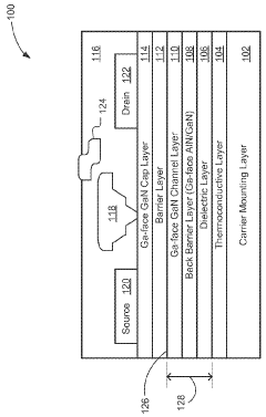
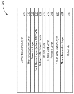
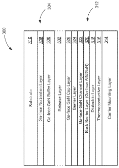
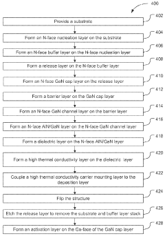
Gallium nitride on high thermal conductivity material device and method
PatentActiveUS9337278B1
Innovation
- The approach involves forming GaN high electron mobility transistors (HEMTs) using a Ga-face wafer stack with a thermoconductive layer and a back barrier layer, where the high thermal conductivity material is brought close to the junction, reducing thermal resistance and protecting the N-face GaN from harsh processing operations, and using an inverted N-face GaN epitaxial structure with a high thermal conductivity material like diamond bonded to the epitaxial structure.
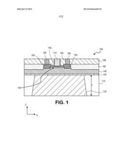
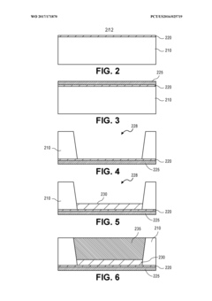
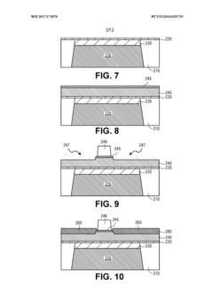
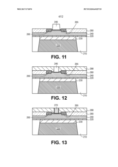
Gallium nitride transistor with underfill aluminum nitride for improved thermal and RF performance
PatentWO2017171870A1
Innovation
- Incorporating an aluminum nitride layer under the gallium nitride transistor or circuit block, utilizing a low resistivity silicon substrate, which provides both high thermal conductivity and high resistivity through the aluminum nitride's insulating properties and superior thermal conductivity compared to silicon.
Reliability Testing Standards for GaN Power Devices
Reliability testing standards for GaN power devices have evolved significantly in response to the unique thermal conductivity challenges these transistors face. The industry has established several key standards that specifically address the thermal management aspects of GaN technology. JEDEC JEP180 and AEC-Q101 have been adapted to include specific provisions for wide bandgap semiconductors, with particular attention to the thermal cycling requirements that reflect GaN's distinctive thermal expansion characteristics.
The IEC 60747 series has incorporated specialized sections for GaN power transistors, with enhanced focus on thermal resistance measurement protocols that account for the material's higher operating temperatures. These standards typically require devices to undergo rigorous thermal shock testing between -55°C and 150°C for a minimum of 1,000 cycles, significantly more demanding than requirements for silicon-based alternatives.
Dynamic thermal performance testing has become a cornerstone of GaN reliability assessment, with standards now mandating pulse testing under various duty cycles to evaluate thermal transient response. This approach better reflects the real-world operating conditions of GaN devices in power conversion applications, where rapid temperature fluctuations are common. The JEDEC JESD51 series has been expanded to address the unique thermal measurement challenges presented by GaN's higher power density.
Accelerated life testing protocols have also been modified to account for GaN's different failure mechanisms. While silicon devices typically undergo testing at 125°C, GaN reliability standards often require testing at temperatures exceeding 150°C to properly stress the material's thermal conductivity limits. These tests typically run for 1,000 hours under maximum rated voltage conditions while monitoring for parametric drift.
Industry consortia like the JEDEC JC-70 Wide Bandgap Power Electronic Conversion Semiconductors committee have been instrumental in developing GaN-specific reliability standards. Their work has led to the creation of specialized test methods that address the unique thermal interface materials required for GaN devices and the evaluation of thermal boundary resistance, which is particularly critical given GaN's thermal conductivity limitations.
Mission profile-based reliability testing has gained prominence, with standards now recommending application-specific thermal cycling regimes that simulate actual deployment conditions. This approach has proven particularly valuable for automotive and industrial applications where GaN devices may experience extreme temperature variations and thermal stress during operation.
Environmental Impact of GaN vs Silicon Technologies
The environmental implications of Gallium Nitride (GaN) technology compared to traditional silicon-based semiconductors represent a critical consideration in the broader adoption of GaN transistors. GaN technology demonstrates significant environmental advantages through its superior energy efficiency. When implemented in power conversion systems, GaN transistors operate at higher frequencies with lower switching losses, resulting in power conversion efficiencies exceeding 95%, compared to silicon's typical 85-90%. This efficiency translates directly to reduced energy consumption and lower carbon emissions across various applications including data centers, electric vehicles, and renewable energy systems.
Manufacturing processes for GaN devices have evolved to become increasingly environmentally responsible. While early production methods involved resource-intensive techniques, modern epitaxial growth processes have reduced waste generation by approximately 30% compared to traditional silicon manufacturing. Additionally, GaN devices require smaller die sizes for equivalent performance, resulting in more efficient material utilization and reduced semiconductor waste.
The lifecycle assessment of GaN versus silicon technologies reveals compelling environmental benefits. GaN-based power systems demonstrate a carbon footprint reduction of 25-40% over their operational lifetime compared to silicon equivalents. This advantage stems primarily from reduced energy losses during operation rather than from manufacturing efficiencies. Furthermore, the extended operational temperature range of GaN devices (up to 250°C versus silicon's 150°C) contributes to longer product lifespans, reducing electronic waste generation.
Resource utilization presents both challenges and opportunities. While gallium is less abundant than silicon, the minimal quantities required for GaN device fabrication mitigate supply concerns. Recent recycling innovations have demonstrated up to 65% recovery rates for gallium from end-of-life electronics, creating potential circular economy opportunities. Additionally, GaN devices require significantly fewer rare earth elements compared to some alternative semiconductor technologies.
Thermal management solutions for GaN transistors have environmental implications as well. Advanced cooling systems necessary for high-power GaN applications typically utilize less environmentally harmful materials compared to traditional cooling compounds. The elimination of lead-based solders in GaN packaging aligns with global initiatives to reduce hazardous substances in electronics manufacturing.
As GaN technology continues to mature, its environmental profile improves through manufacturing optimization and increased adoption in energy-critical applications. The technology's contribution to enabling more efficient renewable energy systems and electric transportation further amplifies its positive environmental impact, potentially offsetting its production footprint within months of deployment in high-efficiency applications.
Unlock deeper insights with Patsnap Eureka Quick Research — get a full tech report to explore trends and direct your research. Try now!
Generate Your Research Report Instantly with AI Agent
Supercharge your innovation with Patsnap Eureka AI Agent Platform!