Gallium Nitride Transistors and Their Influence on Global Electronics Market
OCT 14, 20259 MIN READ
Generate Your Research Report Instantly with AI Agent
Patsnap Eureka helps you evaluate technical feasibility & market potential.
GaN Transistor Evolution and Objectives
Gallium Nitride (GaN) transistors represent a revolutionary advancement in semiconductor technology, emerging as a viable alternative to traditional silicon-based transistors. The evolution of GaN technology began in the early 1990s with fundamental research into wide-bandgap semiconductors, but significant commercial development only gained momentum in the early 2000s when researchers overcame critical material growth and fabrication challenges.
The inherent properties of GaN provide substantial advantages over silicon, including higher breakdown voltage, faster switching speeds, higher thermal conductivity, and lower on-resistance. These characteristics enable GaN transistors to operate at higher frequencies, temperatures, and power densities while maintaining greater efficiency. The technology has evolved through several generations, from early experimental devices to today's commercially available high-electron-mobility transistors (HEMTs) and enhancement-mode GaN transistors.
A pivotal milestone in GaN evolution occurred around 2010 when manufacturers developed reliable methods for growing high-quality GaN on silicon substrates, dramatically reducing production costs and enabling broader commercial adoption. This breakthrough transformed GaN from a niche technology primarily used in defense and aerospace applications to a commercially viable solution for consumer and industrial electronics.
The current technological trajectory shows GaN transistors advancing along multiple dimensions simultaneously: increasing power handling capabilities, improving reliability, reducing costs, and expanding integration capabilities. Recent innovations include monolithic integration of GaN power devices with control circuitry and the development of vertical GaN structures for ultra-high-power applications.
The primary objectives driving GaN transistor development include achieving higher power density to enable smaller form factors in power electronics, improving energy efficiency to meet increasingly stringent environmental regulations, and reducing manufacturing costs to compete more effectively with silicon technologies. Additional goals include enhancing reliability for mission-critical applications and developing specialized variants optimized for specific applications such as RF communications, automotive systems, and renewable energy.
Looking forward, the GaN transistor roadmap aims to further expand operating parameters, with targets including breakdown voltages exceeding 1800V for high-power applications, switching frequencies above 100MHz for more compact power conversion systems, and on-resistance approaching theoretical limits. Researchers are also pursuing novel device architectures, improved thermal management techniques, and advanced packaging solutions to maximize the technology's potential.
The ultimate objective is to establish GaN as the dominant technology for next-generation power electronics and RF applications, fundamentally transforming global electronics markets through superior performance, efficiency, and reliability compared to conventional silicon-based solutions.
Market Demand Analysis for GaN-Based Electronics
The global market for Gallium Nitride (GaN) transistors has witnessed remarkable growth in recent years, driven primarily by the increasing demand for high-performance electronic devices across various sectors. The power electronics market, valued at approximately $40 billion in 2022, is projected to reach $73 billion by 2027, with GaN-based devices capturing an increasingly significant share of this expanding market.
Consumer electronics represents one of the largest application segments for GaN transistors, particularly in fast chargers for smartphones, tablets, and laptops. The superior power efficiency of GaN enables manufacturers to produce smaller, lighter, and more energy-efficient charging solutions. Market analysis indicates that GaN charger adoption is growing at over 50% annually, with major brands like Apple, Samsung, and Xiaomi incorporating this technology into their product ecosystems.
The automotive sector presents another substantial growth opportunity for GaN transistors. With electric vehicles (EVs) gaining mainstream acceptance, the demand for efficient power conversion systems has intensified. GaN-based power electronics offer significant advantages in EV onboard chargers, DC-DC converters, and inverters, potentially extending vehicle range by 5-10% through improved efficiency. Industry forecasts suggest that by 2026, over 30% of premium EVs will incorporate GaN technology in their power systems.
Telecommunications infrastructure, particularly with the global rollout of 5G networks, constitutes a critical market for GaN RF devices. The superior power handling capabilities and frequency response of GaN transistors make them ideal for 5G base stations, where they deliver higher data rates while consuming less power than traditional silicon-based solutions. The 5G infrastructure market is expected to grow at a CAGR of 34.2% from 2022 to 2027, creating substantial demand for GaN RF components.
Industrial applications represent an emerging but rapidly growing segment for GaN technology. Factory automation systems, industrial power supplies, and motor drives benefit from the higher switching frequencies and reduced energy losses offered by GaN transistors. This sector is projected to adopt GaN solutions at an accelerating pace as manufacturers seek to meet increasingly stringent energy efficiency regulations and reduce operational costs.
Regional analysis reveals that Asia-Pacific currently dominates the GaN market, accounting for approximately 45% of global demand, followed by North America at 30% and Europe at 20%. China, Japan, South Korea, and Taiwan are particularly significant markets due to their robust electronics manufacturing ecosystems. However, North America leads in GaN innovation and high-end applications, while Europe shows strong growth potential in automotive and industrial implementations.
GaN Technology Status and Barriers
Gallium Nitride (GaN) technology has emerged as a revolutionary material in the semiconductor industry, offering significant advantages over traditional silicon-based technologies. Currently, GaN transistors are being commercially deployed in various high-frequency and high-power applications, with major advancements in RF communications, power electronics, and LED lighting. The global market adoption is accelerating, particularly in 5G infrastructure, electric vehicles, and renewable energy systems where efficiency and power density are critical factors.
Despite its promising potential, GaN technology faces several significant barriers to widespread adoption. Manufacturing challenges remain a primary concern, as GaN wafer production costs substantially exceed those of silicon. The industry continues to struggle with defect densities in GaN epitaxial layers, which affect device reliability and yield rates. Current manufacturing processes typically utilize 6-inch wafers, whereas silicon technology has advanced to 12-inch wafers, creating a scaling disadvantage for GaN production economics.
Technical barriers also persist in device design and implementation. Thermal management represents a critical challenge, as GaN devices generate significant heat during high-power operation. Current packaging technologies often fail to efficiently dissipate this heat, limiting the performance potential of GaN transistors. Additionally, gate reliability issues and dynamic Ron effects (current collapse phenomena) continue to impact long-term stability in certain applications, requiring complex compensation circuits that increase system complexity.
From a market perspective, the GaN ecosystem remains less mature than silicon, with fewer suppliers, design tools, and supporting components specifically optimized for GaN implementation. This creates integration challenges for system designers attempting to incorporate GaN technology into established product architectures. The higher initial component cost of GaN devices compared to silicon equivalents also presents a barrier to adoption in cost-sensitive markets, despite the potential for system-level cost savings through increased efficiency and reduced cooling requirements.
Geographically, GaN technology development shows distinct regional patterns. The United States and Japan lead in fundamental research and intellectual property, while Taiwan and China have made significant investments in manufacturing capacity. Europe maintains strength in automotive and industrial applications of GaN technology. This distributed expertise creates both collaboration opportunities and competitive tensions in the global supply chain.
Regulatory and standardization gaps further complicate GaN adoption. The unique characteristics of GaN devices require updated testing methodologies and reliability standards, which are still evolving. Additionally, electromagnetic compatibility regulations may need revision to accommodate the faster switching speeds and higher frequencies enabled by GaN technology.
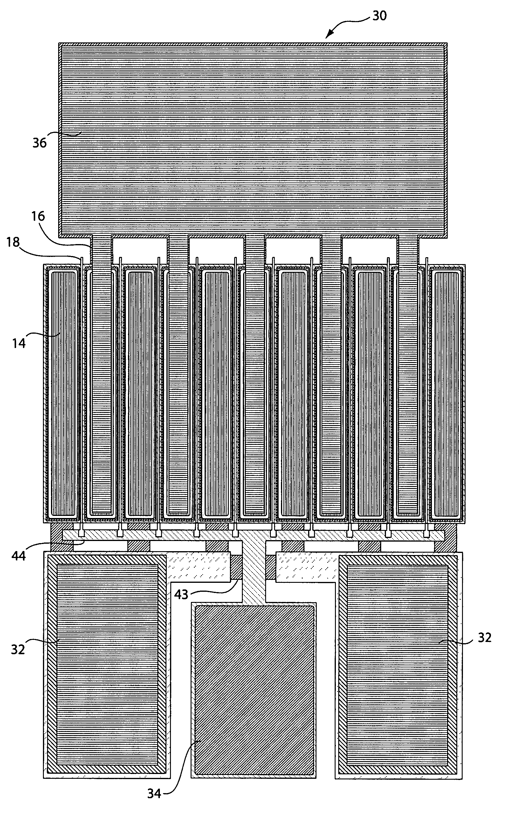
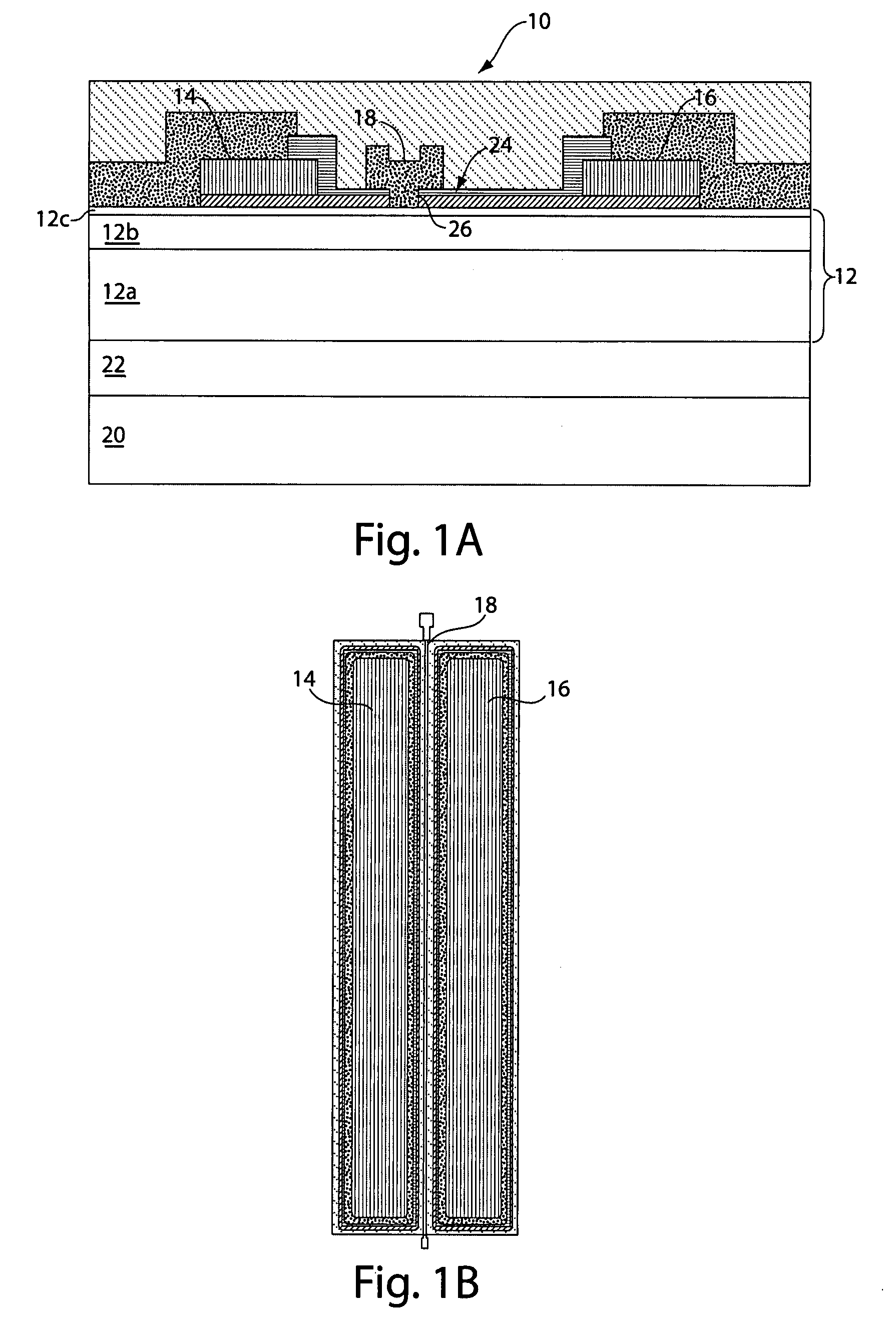
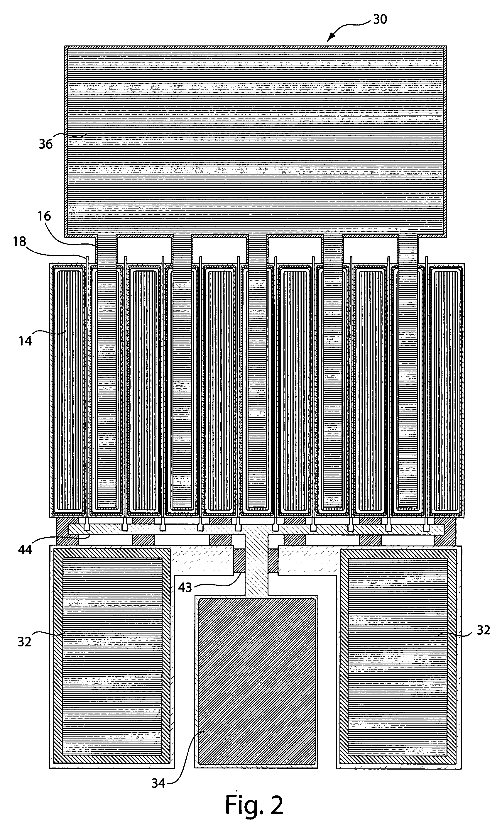
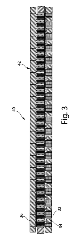
Current GaN Transistor Solutions
01 Fabrication methods for GaN transistors
Various methods for manufacturing gallium nitride transistors, including epitaxial growth techniques, substrate preparation, and device fabrication processes. These methods focus on improving crystal quality, reducing defects, and enhancing device performance. Specific techniques include MOCVD growth, substrate selection, and specialized processing steps to create high-quality GaN transistor structures.- Fabrication methods for GaN transistors: Various fabrication methods are employed to create high-quality gallium nitride transistors. These include specialized epitaxial growth techniques, substrate preparation processes, and methods to reduce defect density in the GaN layers. Advanced deposition techniques help achieve optimal crystal structure and electrical properties, while specific etching and patterning processes are used to define device features with precision.
- Device structures for high-performance GaN transistors: Innovative device structures enhance the performance of gallium nitride transistors. These include specialized gate configurations, channel designs, and buffer layer architectures that improve electron mobility and reduce parasitic effects. Heterojunction structures like AlGaN/GaN are commonly employed to create high electron mobility transistors (HEMTs) with superior switching characteristics and power handling capabilities.
- Substrate technologies for GaN transistors: The choice and preparation of substrate materials significantly impact GaN transistor performance. Silicon, silicon carbide, and sapphire substrates are commonly used, each offering different advantages in terms of cost, thermal conductivity, and lattice matching. Advanced substrate engineering techniques help mitigate issues related to lattice mismatch and thermal expansion differences between GaN and the substrate material.
- Power applications and performance optimization: Gallium nitride transistors excel in power electronics applications due to their wide bandgap properties. Specific design optimizations focus on enhancing breakdown voltage, reducing on-resistance, and improving thermal management for high-power operation. Advanced field plate structures, edge termination techniques, and specialized packaging solutions help maximize power handling capabilities while maintaining reliability under high-voltage and high-temperature conditions.
- RF and high-frequency GaN transistor designs: Gallium nitride transistors are engineered for superior radio frequency and high-frequency performance. Specialized designs incorporate features to minimize parasitic capacitances and inductances, optimize gate structures for high-frequency operation, and enhance linearity for communication applications. These transistors achieve high power density and efficiency at microwave and millimeter-wave frequencies, making them ideal for radar, wireless communications, and satellite systems.
02 High electron mobility transistor (HEMT) structures
Design and implementation of GaN-based high electron mobility transistors, which utilize the two-dimensional electron gas formed at the interface between GaN and AlGaN layers. These structures offer high electron mobility, high breakdown voltage, and excellent high-frequency performance. Various architectural improvements focus on enhancing channel conductivity, reducing parasitic effects, and optimizing gate control.Expand Specific Solutions03 Substrate technologies for GaN devices
Development of substrate technologies specifically for gallium nitride transistors, including silicon carbide, sapphire, and silicon substrates. These technologies address challenges such as lattice mismatch, thermal expansion differences, and defect reduction. Advanced substrate engineering techniques help improve device performance, reliability, and thermal management while potentially reducing manufacturing costs.Expand Specific Solutions04 Power electronics applications
Implementation of gallium nitride transistors in power electronic applications, leveraging their high breakdown voltage, low on-resistance, and fast switching capabilities. These devices enable more efficient power conversion systems with higher operating frequencies and reduced form factors. Specific designs address thermal management, reliability under high-voltage operation, and integration with existing power systems.Expand Specific Solutions05 Enhancement and depletion mode GaN transistors
Design and fabrication of both enhancement-mode (normally-off) and depletion-mode (normally-on) gallium nitride transistors for different application requirements. Enhancement-mode devices are preferred for safety and compatibility with existing circuits, while depletion-mode devices offer certain performance advantages. Various gate structures and channel modifications are employed to achieve the desired threshold voltage characteristics.Expand Specific Solutions
Key Industry Players in GaN Semiconductor Market
The Gallium Nitride (GaN) transistor market is experiencing rapid growth in the global electronics sector, currently transitioning from early adoption to mainstream implementation. The market is projected to expand significantly, driven by GaN's superior performance characteristics over silicon in high-power, high-frequency applications. Key players demonstrate varying levels of technological maturity: established semiconductor leaders like Intel, Texas Instruments, and NXP are integrating GaN into their product portfolios, while specialized firms such as GaN Systems, Transphorm, and Innoscience are pushing innovation boundaries. Research institutions including CEA, Xidian University, and Southeast University are advancing fundamental GaN technology. The competitive landscape is diversifying as Asian manufacturers like United Microelectronics and Hangzhou Silan challenge traditional Western dominance, indicating a globally distributed technology ecosystem with multiple centers of excellence.
GaN Systems, Inc.
Technical Solution: GaN Systems specializes in gallium nitride power transistors, offering a comprehensive portfolio of GaN power semiconductors. Their Island Technology® design uses a proprietary cell layout that maximizes current handling capability while minimizing thermal resistance. The company's GaNPX® packaging eliminates wire bonds and provides superior thermal performance, enabling higher switching frequencies up to 100MHz compared to silicon's typical 100kHz limit. Their devices operate at junction temperatures up to 175°C with breakdown voltages exceeding 1200V. GaN Systems' transistors demonstrate a Figure of Merit (RDS(on) × QG) approximately 4-10 times better than silicon alternatives, significantly reducing switching losses in power conversion applications.
Strengths: Industry-leading power density; near-zero switching losses; superior thermal performance; enables smaller, lighter power systems. Weaknesses: Higher initial cost compared to silicon; requires redesign of existing power circuits; relatively new technology with less established reliability data compared to mature silicon solutions.
Innoscience Suzhou Semiconductor Co. Ltd.
Technical Solution: Innoscience has established itself as the world's largest dedicated 8-inch GaN-on-Silicon manufacturing facility, with a monthly capacity exceeding 10,000 wafers. Their InnoGaN® technology platform features both enhancement-mode (E-mode) and depletion-mode (D-mode) GaN HEMTs, with proprietary processing techniques that achieve threshold voltage stability within ±100mV. The company's innovative "all-in-one" integration approach combines multiple GaN devices on a single chip, reducing parasitic inductances and enabling higher power density solutions. Innoscience's low-voltage (30-150V) GaNInside™ technology targets consumer electronics, while their high-voltage (650V+) solutions address industrial power supplies and automotive applications. Their advanced epitaxial growth techniques achieve dislocation densities below 10^8 cm^-2, contributing to enhanced device reliability and performance consistency across large wafers.
Strengths: Massive manufacturing scale providing cost advantages; comprehensive product portfolio spanning 30V-650V; vertically integrated from epitaxy to finished products; strong presence in consumer electronics market. Weaknesses: Relatively new entrant to global markets; less established brand recognition outside China; limited third-party validation data compared to longer-established competitors.
Critical GaN Patents and Technical Innovations
Gallium nitride material transistors and methods for wideband applications
PatentInactiveUS20070202360A1
Innovation
- The development of gallium nitride material transistors with active regions formed in gallium nitride layers, integrated with matching circuits to achieve low relative constellation error (RCE) values and high efficiency, enabling efficient signal amplification and transmission with excellent linearity and compliance with spectrum mask requirements.
Gallium nitride high electron mobility transistor
PatentInactiveUS20230411509A1
Innovation
- Incorporating p-type gallium nitride islands between the gate and drain electrodes, which act as electrically floating islands to recombine redundant electrons on the barrier layer, thereby maintaining the concentration of two-dimensional electron gas and enhancing the transistor's reliability.
Supply Chain Resilience for GaN Materials
The global supply chain for Gallium Nitride (GaN) materials faces unique challenges that require strategic approaches to ensure resilience. The primary raw material, gallium, is predominantly obtained as a byproduct of aluminum and zinc processing, with China controlling approximately 80% of global gallium production. This geographic concentration creates inherent vulnerabilities in the supply chain, particularly evident during recent export restrictions that sent shockwaves through the semiconductor industry.
To address these vulnerabilities, diversification of gallium sources has become a critical strategy. Countries including Japan, South Korea, and Germany are investing in alternative extraction methods and recycling technologies to reduce dependence on Chinese supplies. The European Union has designated gallium as a critical raw material, allocating significant funding for research into sustainable sourcing options through its Horizon Europe program.
Vertical integration represents another approach to supply chain resilience, with major GaN semiconductor manufacturers increasingly securing their supply chains through strategic partnerships or direct investments in material processing facilities. Companies like Infineon Technologies and Wolfspeed have established long-term agreements with material suppliers to ensure consistent access to high-quality GaN substrates and epitaxial wafers.
Technological innovations are also contributing to supply chain resilience. Advanced recycling processes can now recover up to 85% of gallium from manufacturing waste and end-of-life electronics, significantly reducing reliance on primary sources. Additionally, research into alternative substrate materials such as silicon carbide and diamond is progressing, potentially offering complementary pathways for GaN device manufacturing when traditional materials face supply constraints.
Stockpiling has emerged as a short-term strategy, with both governments and private enterprises maintaining strategic reserves of gallium and GaN materials. Japan's rare metals stockpiling program, for instance, maintains reserves sufficient for several months of national consumption, providing a buffer against supply disruptions.
International cooperation frameworks are developing to address supply chain vulnerabilities. The U.S.-Japan Critical Minerals Partnership and similar initiatives aim to coordinate efforts in securing stable supplies of critical materials including gallium. These collaborative approaches include joint research programs, coordinated investment strategies, and harmonized regulatory frameworks to facilitate smoother material flows across borders.
The resilience of GaN material supply chains will significantly influence the pace of adoption for GaN transistors in global electronics markets. As manufacturers implement these multi-faceted strategies, the industry is gradually moving toward a more robust supply ecosystem that can withstand geopolitical tensions and market volatility.
Environmental Impact of GaN vs Silicon Technologies
The environmental impact of GaN (Gallium Nitride) technology compared to traditional silicon-based technologies represents a critical consideration in the ongoing transition of the global electronics market. GaN transistors demonstrate significant environmental advantages throughout their lifecycle, beginning with manufacturing processes that require fewer chemical inputs and generate less toxic waste compared to silicon technologies. The production of GaN devices typically consumes 10-15% less energy than equivalent silicon components, contributing to reduced carbon emissions during the manufacturing phase.
In operational contexts, GaN transistors deliver substantial environmental benefits through their superior energy efficiency. Systems utilizing GaN technology consistently demonstrate 40-50% lower energy consumption compared to silicon-based alternatives, particularly in high-power applications such as data centers, telecommunications infrastructure, and electric vehicle charging systems. This efficiency translates directly into reduced greenhouse gas emissions and lower resource consumption across the electronics ecosystem.
The thermal management requirements for GaN devices are markedly reduced due to their ability to operate at higher temperatures with less performance degradation. This characteristic allows for smaller cooling systems and heat sinks, decreasing the overall material footprint of electronic products. Research indicates that GaN-based power systems can reduce cooling infrastructure requirements by up to 30%, resulting in significant materials conservation and associated environmental benefits.
Product lifespan represents another environmental advantage of GaN technology. The superior reliability and resilience of GaN transistors under thermal and electrical stress extend operational lifetimes by an estimated 3-5 years beyond comparable silicon devices. This longevity reduces electronic waste generation and mitigates the environmental impact associated with manufacturing replacement components.
End-of-life considerations also favor GaN technology, though challenges remain. While both silicon and GaN components contain materials requiring specialized recycling processes, the higher energy efficiency of GaN devices throughout their operational life typically offsets the environmental impact of their disposal. However, the gallium content in GaN devices presents specific recycling challenges that the industry continues to address through developing specialized recovery processes.
From a holistic environmental perspective, lifecycle assessments indicate that GaN-based electronic systems can reduce overall carbon footprint by 25-40% compared to silicon alternatives when considering manufacturing, operation, and disposal phases collectively. This significant environmental advantage positions GaN technology as a key enabler for sustainable electronics development and aligns with global initiatives to reduce the environmental impact of the technology sector.
Unlock deeper insights with Patsnap Eureka Quick Research — get a full tech report to explore trends and direct your research. Try now!
Generate Your Research Report Instantly with AI Agent
Supercharge your innovation with Patsnap Eureka AI Agent Platform!