How Industry Regulations Influence Gallium Nitride Transistor Adoption
OCT 14, 20259 MIN READ
Generate Your Research Report Instantly with AI Agent
Patsnap Eureka helps you evaluate technical feasibility & market potential.
GaN Transistor Development History and Objectives
Gallium Nitride (GaN) transistor technology has evolved significantly since its inception in the early 1990s. The journey began with fundamental research at universities and research institutions focusing on the unique properties of GaN as a wide-bandgap semiconductor material. Initial development faced substantial challenges related to material quality, substrate availability, and fabrication techniques, limiting early adoption to specialized applications.
The mid-2000s marked a pivotal turning point when researchers successfully demonstrated enhanced electron mobility and power handling capabilities in GaN high-electron-mobility transistors (HEMTs). This breakthrough catalyzed increased investment from both government agencies and private corporations, particularly in defense and telecommunications sectors where the superior frequency performance of GaN devices offered significant advantages.
By 2010, commercial GaN transistors began emerging in the market, primarily targeting RF applications in cellular infrastructure and military radar systems. The technology's evolution accelerated as manufacturing processes matured, gradually reducing production costs while improving reliability metrics. This period saw the establishment of key technical standards and performance benchmarks that would later influence regulatory frameworks.
The 2015-2020 timeframe witnessed GaN transistors expanding into broader power electronics applications, challenging traditional silicon-based solutions in areas requiring high efficiency and power density. This expansion coincided with growing regulatory focus on energy efficiency across multiple industries, creating both opportunities and compliance challenges for GaN adoption.
Current technical objectives for GaN transistor development center on several key areas: improving reliability under extreme operating conditions, reducing manufacturing costs to compete with silicon technologies, enhancing integration capabilities for system-on-chip solutions, and addressing thermal management challenges inherent to high-power density applications.
Looking forward, the technology roadmap aims to achieve wider voltage operating ranges (particularly at higher voltages exceeding 1200V), further miniaturization while maintaining thermal performance, and development of application-specific variants optimized for emerging markets like electric vehicles and renewable energy systems.
The evolution of GaN transistor technology continues to be shaped by a complex interplay between technical innovation, manufacturing economics, and increasingly, regulatory frameworks across different industries. As energy efficiency regulations tighten globally, GaN transistors are positioned as a key enabling technology for meeting these requirements, though their adoption path remains influenced by industry-specific certification processes and safety standards that were originally developed for silicon-based technologies.
Market Analysis for GaN Power Electronics
The global market for Gallium Nitride (GaN) power electronics has experienced remarkable growth in recent years, with a compound annual growth rate exceeding 40% since 2018. This surge is primarily driven by the superior performance characteristics of GaN transistors compared to traditional silicon-based alternatives, including higher switching speeds, greater power density, and improved thermal efficiency.
Consumer electronics represents the largest current market segment for GaN power electronics, accounting for approximately 35% of total market share. This dominance stems from the increasing demand for fast-charging solutions in smartphones, tablets, and laptops, where GaN's efficiency translates to smaller, lighter power adapters with reduced charging times.
Automotive applications constitute the fastest-growing segment, with projections indicating a 55% annual growth rate through 2026. The transition toward electric vehicles has created substantial demand for high-efficiency power conversion systems where GaN excels. Major automotive manufacturers have begun incorporating GaN-based onboard chargers and DC-DC converters to improve vehicle range and reduce charging infrastructure costs.
Industrial power systems represent another significant market opportunity, particularly in renewable energy applications. GaN-based inverters for solar panels demonstrate efficiency improvements of 2-3 percentage points over silicon alternatives, which translates to substantial energy savings at scale. Similarly, wind power systems benefit from GaN's ability to handle higher voltages with reduced switching losses.
Telecommunications infrastructure, particularly with the ongoing 5G rollout, has emerged as a critical market for GaN power electronics. Base stations utilizing GaN technology consume approximately 20% less power while delivering improved signal quality and coverage range. This efficiency becomes increasingly important as network densification continues.
Regional analysis reveals North America currently leads in GaN adoption, representing 38% of the global market, followed by Asia-Pacific at 35% and Europe at 22%. However, the Asia-Pacific region is expected to overtake North America by 2025, driven by aggressive manufacturing investments in China, Taiwan, and South Korea.
Pricing trends show steady improvement, with the cost premium of GaN solutions over silicon alternatives decreasing from approximately 300% in 2015 to 40-60% today. Industry analysts project price parity with silicon in specific high-volume applications by 2024, which would significantly accelerate adoption across all market segments.
Global GaN Technology Status and Barriers
Gallium Nitride (GaN) technology has emerged as a revolutionary material in power electronics, offering significant advantages over traditional silicon-based semiconductors. Currently, GaN technology has reached commercial maturity in several applications, particularly in power conversion, RF amplifiers, and LED lighting. The global market for GaN power devices is experiencing robust growth, with a compound annual growth rate exceeding 20% according to recent market analyses.
Despite this progress, GaN technology faces several significant barriers to widespread adoption. Technical challenges remain prominent, including issues with current collapse phenomena, dynamic on-resistance, and reliability concerns under high-voltage switching conditions. These technical limitations have slowed adoption in mission-critical applications where long-term reliability data is essential.
Manufacturing scalability represents another substantial barrier. The production of high-quality GaN epitaxial layers on various substrates (silicon, silicon carbide, or native GaN) continues to present yield challenges and cost implications. While silicon substrates offer cost advantages, they introduce additional complexities in managing stress and defect density in GaN layers.
Regulatory frameworks across different regions have created a fragmented landscape for GaN technology implementation. In the United States, the Department of Defense has classified certain GaN technologies as strategically important, subjecting them to export controls under International Traffic in Arms Regulations (ITAR). This has limited international collaboration and technology transfer in military and aerospace applications.
The European Union has implemented the RoHS (Restriction of Hazardous Substances) and REACH (Registration, Evaluation, Authorization and Restriction of Chemicals) regulations, which impact GaN manufacturing processes and supply chains. While GaN itself is not restricted, certain processing chemicals and manufacturing byproducts require careful management to ensure compliance.
In Asia, particularly China, government initiatives have heavily invested in developing domestic GaN technology capabilities, creating a competitive landscape with varying regulatory standards. Japan and South Korea have established advanced GaN research programs with strong industry-academic partnerships, accelerating technology development within their regulatory frameworks.
Standardization remains an ongoing challenge globally. The lack of unified testing protocols and performance metrics for GaN devices has created market uncertainty and hampered adoption in conservative industries such as automotive and industrial power systems. Organizations like JEDEC and IEC are working to establish standards, but progress has been slower than technology development.
Access to intellectual property presents another significant barrier, with key patents concentrated among a relatively small number of companies and research institutions. This concentration has created licensing challenges for new entrants and smaller companies seeking to develop GaN-based products.
Current GaN Transistor Implementation Solutions
01 Manufacturing techniques for GaN transistors
Various manufacturing techniques have been developed to improve the production of gallium nitride transistors. These include specialized growth methods for GaN crystals, substrate preparation processes, and fabrication techniques that enhance device performance and reliability. Advanced epitaxial growth methods and precise control of material properties during manufacturing contribute to higher quality GaN transistors suitable for commercial adoption.- GaN Transistor Manufacturing Techniques: Various manufacturing techniques have been developed to produce high-quality gallium nitride transistors. These include specialized epitaxial growth methods, substrate preparation processes, and device fabrication techniques that enhance the performance and reliability of GaN transistors. Advanced manufacturing approaches help overcome challenges related to crystal defects and enable the production of transistors with superior electrical properties.
- GaN HEMT Device Structures: High Electron Mobility Transistor (HEMT) structures based on gallium nitride offer significant advantages for power and RF applications. These structures typically feature AlGaN/GaN heterojunctions that create a two-dimensional electron gas with high carrier mobility. Various design innovations in gate configuration, field plates, and buffer layers have been implemented to enhance breakdown voltage, reduce leakage current, and improve thermal performance.
- GaN Transistor Applications in Power Electronics: Gallium nitride transistors are increasingly adopted in power electronics applications due to their superior switching characteristics and high breakdown voltage. These devices enable more efficient power conversion systems with higher operating frequencies and reduced form factors. Key applications include power supplies, motor drives, renewable energy inverters, and automotive electronics, where GaN transistors offer significant efficiency improvements over silicon-based alternatives.
- GaN Material Growth and Substrate Technologies: The quality of gallium nitride material is critical for transistor performance. Various approaches have been developed for growing high-quality GaN crystals, including MOCVD and HVPE techniques. Substrate technologies have evolved from sapphire and silicon carbide to native GaN substrates and engineered silicon substrates. These advancements address challenges related to lattice mismatch, thermal expansion differences, and defect density reduction.
- GaN Transistor Reliability and Performance Enhancement: Ensuring the long-term reliability of gallium nitride transistors is essential for widespread adoption. Research has focused on addressing degradation mechanisms such as current collapse, gate leakage, and thermal management issues. Various passivation techniques, surface treatments, and field management structures have been developed to enhance device stability. Performance enhancements include reduced on-resistance, improved switching speed, and better thermal conductivity.
02 GaN transistor device structures
Innovative device structures have been developed to optimize the performance of GaN transistors. These include various gate configurations, channel designs, and layer structures that enhance electron mobility and power handling capabilities. Structural innovations such as heterojunction designs, field plates, and novel contact arrangements help overcome traditional limitations of semiconductor devices and enable the widespread adoption of GaN technology in power electronics applications.Expand Specific Solutions03 Integration of GaN with existing semiconductor technologies
Methods for integrating gallium nitride transistors with conventional semiconductor technologies have been developed to facilitate adoption. These approaches include techniques for growing GaN on silicon substrates, hybrid integration methods, and compatible processing techniques that allow GaN devices to be incorporated into established manufacturing flows. Such integration strategies are crucial for the commercial adoption of GaN transistors in mainstream electronics applications.Expand Specific Solutions04 Performance enhancements for GaN power devices
Various techniques have been developed to enhance the performance characteristics of GaN transistors, particularly for power applications. These include methods to increase breakdown voltage, reduce on-resistance, improve thermal management, and enhance switching speed. Such performance enhancements are critical for the adoption of GaN transistors in high-power and high-frequency applications where they offer significant advantages over traditional silicon-based devices.Expand Specific Solutions05 Material quality improvements for GaN semiconductors
Advancements in material quality have been crucial for the adoption of GaN transistors. These include methods to reduce defect density, improve crystal quality, and enhance the purity of gallium nitride materials. Techniques for substrate preparation, buffer layer growth, and doping control contribute to higher performance and reliability of GaN transistors, making them more suitable for commercial applications across various industries.Expand Specific Solutions
Leading GaN Semiconductor Companies and Competition
The gallium nitride (GaN) transistor market is currently in a growth phase, with increasing adoption across power electronics applications despite regulatory complexities. The market is projected to expand significantly as GaN technology offers superior performance over traditional silicon-based solutions. Leading semiconductor manufacturers including Wolfspeed, NXP, MACOM, and Texas Instruments are driving innovation, while companies like Intel and Huawei are integrating GaN solutions into their product ecosystems. Asian players such as TSMC and Innoscience are establishing strong positions in manufacturing capabilities. Regulatory frameworks across different regions influence adoption rates, with standards for efficiency, electromagnetic compatibility, and reliability creating both challenges and opportunities for market participants as the technology matures toward mainstream commercialization.
Huawei Technologies Co., Ltd.
Technical Solution: Huawei has developed a regulatory-aware approach to GaN transistor implementation focusing on telecommunications infrastructure and power systems. Their strategy involves GaN-on-Si technology to address cost concerns while meeting efficiency regulations in data centers and 5G base stations. Huawei's GaN transistors are designed with specific attention to international safety standards including IEC 62368 for ICT equipment. Their devices incorporate advanced thermal management techniques to comply with operational temperature limits in various deployment environments. Huawei has established specialized testing facilities to validate GaN transistor performance under various regulatory scenarios, including electromagnetic compatibility testing to meet regional EMC directives. Their approach includes developing region-specific variants of GaN power systems to address divergent regulatory requirements across global markets, particularly navigating the complex regulatory landscape between Western markets and China.
Strengths: Strong vertical integration from device to system level enabling optimized regulatory compliance; extensive experience navigating divergent international standards. Weaknesses: Geopolitical challenges affecting market access in certain regions; regulatory uncertainty regarding technology transfer restrictions.
Texas Instruments Incorporated
Technical Solution: Texas Instruments has developed a regulation-centric approach to GaN transistor technology focusing on power management applications across multiple industries. Their GaN implementation strategy addresses efficiency regulations through 600V-rated devices that exceed Energy Star and similar global efficiency standards. TI's GaN transistors incorporate advanced gate driver technology that ensures compliance with conducted and radiated emission standards while maintaining high switching frequencies. Their devices feature integrated protection mechanisms that address safety requirements in consumer, industrial and automotive applications, meeting standards like UL/IEC 62368. TI has established comprehensive qualification methodologies that address reliability concerns raised by regulatory bodies, with accelerated life testing protocols that simulate decades of operation under various environmental conditions. Their approach includes detailed application guidance to help customers implement GaN solutions that meet regulatory requirements across different regions, with particular attention to emerging standards in energy efficiency.
Strengths: Extensive power management ecosystem enabling compliant system-level solutions; robust reliability qualification data accepted by regulatory bodies worldwide. Weaknesses: More conservative voltage/current ratings compared to specialized GaN competitors; regulatory compliance features add complexity to implementation.
Key Patents and Technical Innovations in GaN Transistors
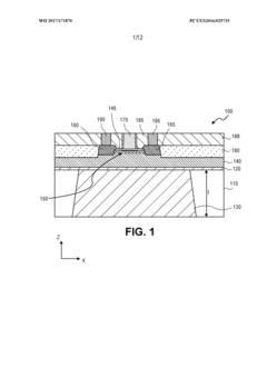
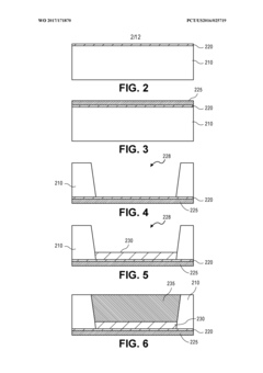
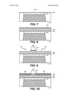
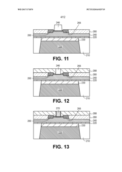
Gallium nitride transistor with underfill aluminum nitride for improved thermal and RF performance
PatentWO2017171870A1
Innovation
- Incorporating an aluminum nitride layer under the gallium nitride transistor or circuit block, utilizing a low resistivity silicon substrate, which provides both high thermal conductivity and high resistivity through the aluminum nitride's insulating properties and superior thermal conductivity compared to silicon.
Gallium nitride voltage regulator
PatentActiveUS20190058041A1
Innovation
- The co-integration of GaN PMOS and NMOS transistors is achieved by growing GaN layers on silicon substrates using shallow trench isolation structures and polarization layers, forming two-dimensional electron gas at the interface, and utilizing magnesium doping for p-doped GaN layers, allowing for the formation of high-breakdown-voltage logic devices and efficient voltage regulation.
Regulatory Framework Impact on GaN Adoption
Regulatory frameworks across different regions significantly shape the adoption trajectory of Gallium Nitride (GaN) transistor technology in commercial and industrial applications. These regulations, which vary considerably between North America, Europe, and Asia-Pacific markets, establish the parameters within which GaN technology must operate, influencing everything from manufacturing processes to end-user implementation.
In the United States, the Department of Energy (DOE) and Federal Communications Commission (FCC) have established efficiency standards and electromagnetic compatibility requirements that indirectly accelerate GaN adoption. The DOE's energy efficiency mandates for power supplies have positioned GaN transistors as an attractive solution due to their superior efficiency characteristics compared to silicon alternatives. Meanwhile, the FCC's stringent electromagnetic interference regulations favor GaN's cleaner switching performance.
European regulatory bodies, particularly through the European Union's Eco-design Directive and RoHS (Restriction of Hazardous Substances) compliance requirements, have created a regulatory environment that generally favors GaN technology. The EU's aggressive carbon reduction targets have incentivized the adoption of more efficient power electronics, creating market pull for GaN solutions. Additionally, the EU's REACH regulation impacts material selection and manufacturing processes for semiconductor technologies.
In Asia, particularly China, Japan, and South Korea, government-backed initiatives often directly promote next-generation semiconductor technologies, including GaN. China's focus on technological self-sufficiency through programs like "Made in China 2025" has accelerated domestic GaN research and production capabilities. Japan's regulatory framework emphasizes energy efficiency in consumer electronics, creating natural market opportunities for GaN implementation.
Defense and aerospace applications face particularly complex regulatory environments, with International Traffic in Arms Regulations (ITAR) and Export Administration Regulations (EAR) significantly impacting global supply chains for GaN technology. These regulations can create barriers to international collaboration and technology transfer, potentially slowing adoption in certain sectors.
Safety certification requirements, such as UL in North America and CE marking in Europe, present both challenges and opportunities for GaN adoption. While these standards ensure product safety, they also require manufacturers to invest in extensive testing and validation processes for new GaN-based designs, potentially extending time-to-market for innovative products.
The evolving nature of these regulatory frameworks creates a dynamic landscape that industry participants must navigate carefully. Companies investing in GaN technology must maintain regulatory intelligence capabilities to anticipate changes and position their product development accordingly. Forward-looking regulatory strategies that anticipate rather than merely react to regulatory developments can provide significant competitive advantages in the rapidly evolving GaN market.
Supply Chain Security Considerations for GaN Components
The security of the GaN component supply chain has emerged as a critical concern for both industry stakeholders and regulatory bodies. As GaN transistors become increasingly vital in defense, telecommunications, and critical infrastructure applications, their supply chains face heightened scrutiny regarding integrity, transparency, and resilience against disruptions or compromises. The concentration of raw material sources presents a significant vulnerability, with China controlling approximately 80% of global gallium production, creating potential geopolitical leverage points that regulatory frameworks must address.
Regulatory bodies worldwide have implemented various measures to mitigate supply chain risks. The U.S. CHIPS Act allocates specific funding for domestic semiconductor manufacturing, including GaN components, while the European Chips Act similarly aims to strengthen regional production capabilities. These initiatives directly influence adoption patterns by creating preferential pathways for domestically produced GaN components in government contracts and critical infrastructure projects.
Verification and certification requirements have become increasingly stringent, with standards such as the Common Criteria for Information Technology Security Evaluation being applied to GaN components in sensitive applications. Companies must now document component origins, manufacturing processes, and testing procedures to meet regulatory compliance, adding complexity to the adoption process but enhancing security assurance.
The implementation of trusted supplier programs represents another regulatory approach affecting GaN adoption. The U.S. Department of Defense's Trusted Foundry Program and similar initiatives in other jurisdictions create approved vendor lists for critical components, effectively channeling adoption toward certified suppliers while potentially limiting market access for non-certified manufacturers, particularly those from regions deemed high-risk.
Trade restrictions and export controls further shape the GaN component landscape. Recent restrictions on semiconductor equipment exports to certain countries have disrupted established supply chains, forcing manufacturers to reconsider sourcing strategies and potentially delaying adoption timelines. These measures reflect growing concerns about technology transfer and the potential dual-use nature of advanced GaN transistors in both commercial and military applications.
Industry response has included the development of more transparent supply chain tracking systems, with blockchain and digital ledger technologies being explored to provide immutable records of component provenance. These innovations, while partly driven by regulatory compliance needs, may ultimately facilitate adoption by building greater trust in supply chain integrity and reducing the risk of counterfeit or compromised components entering critical systems.
Unlock deeper insights with Patsnap Eureka Quick Research — get a full tech report to explore trends and direct your research. Try now!
Generate Your Research Report Instantly with AI Agent
Supercharge your innovation with Patsnap Eureka AI Agent Platform!