Gallium Nitride Transistor Standards in Defense Electronics Applications
OCT 14, 202510 MIN READ
Generate Your Research Report Instantly with AI Agent
Patsnap Eureka helps you evaluate technical feasibility & market potential.
GaN Transistor Evolution and Defense Applications
Gallium Nitride (GaN) transistors have undergone significant evolution since their inception, transforming from experimental devices to critical components in modern defense electronics. The development trajectory began in the early 1990s with rudimentary GaN-based transistors exhibiting limited performance characteristics. These early iterations faced challenges including high defect densities, thermal management issues, and reliability concerns that restricted their practical applications in defense systems.
By the early 2000s, substantial progress in epitaxial growth techniques and device fabrication processes enabled the creation of more robust GaN High Electron Mobility Transistors (HEMTs). This period marked the transition from laboratory curiosities to commercially viable components, with defense contractors beginning to explore their potential for radar and communication systems. The superior electron mobility and high breakdown voltage characteristics of GaN transistors made them particularly attractive for high-power RF applications.
The mid-2000s to early 2010s witnessed accelerated development, with significant improvements in power density, efficiency, and reliability. During this phase, defense applications began incorporating GaN technology into operational systems, particularly in radar modules where their high-power handling capabilities offered substantial advantages over traditional gallium arsenide (GaAs) solutions. The reduced size and weight of GaN-based systems aligned perfectly with the military's emphasis on SWaP (Size, Weight, and Power) optimization.
From 2010 to 2015, GaN transistor technology matured considerably with standardization efforts emerging across the defense industry. Key milestones included the development of radiation-hardened variants for space applications and ruggedized versions capable of withstanding extreme environmental conditions encountered in military deployments. This period also saw the establishment of more robust supply chains and manufacturing processes specifically tailored to defense requirements.
The most recent evolution phase (2015-present) has focused on further refinement of GaN technology for specific defense applications. Advanced thermal management solutions, improved packaging techniques, and enhanced reliability testing protocols have enabled GaN transistors to meet the stringent requirements of mission-critical defense systems. Integration with advanced digital signal processing and AI-driven electronic warfare capabilities has positioned GaN as a cornerstone technology for next-generation defense electronics.
In contemporary defense applications, GaN transistors have become essential components in active electronically scanned array (AESA) radars, electronic warfare systems, secure communications equipment, and missile defense technologies. Their ability to operate at higher frequencies while maintaining power efficiency has revolutionized capabilities in signal jamming, threat detection, and battlefield communications. The technology continues to evolve toward higher operating frequencies, greater power densities, and enhanced integration with other semiconductor technologies to meet emerging defense requirements.
Defense Market Requirements for GaN Transistors
The defense sector imposes stringent requirements on GaN transistors that significantly exceed commercial specifications due to the critical nature of military applications. Reliability under extreme conditions stands as the foremost requirement, with defense systems needing to operate flawlessly in temperature ranges from -55°C to +125°C, far beyond commercial standards. These transistors must withstand intense vibration, shock loads up to 100G, and maintain functionality during rapid thermal cycling without performance degradation.
Radiation hardness represents another crucial defense requirement, as military electronics frequently operate in environments with elevated radiation levels. GaN transistors deployed in defense applications must demonstrate resistance to total ionizing dose (TID) effects, single event upsets (SEUs), and neutron displacement damage, ensuring system integrity during and after radiation exposure.
Long-term operational stability is non-negotiable, with defense contractors typically demanding 15-20 year operational lifespans compared to the 5-7 years accepted in commercial markets. This extended reliability must be maintained without performance drift, requiring specialized aging tests and qualification procedures specific to defense applications.
Power density and efficiency requirements are particularly demanding in defense systems where space and thermal management are constrained. Modern military radar and electronic warfare systems require GaN transistors capable of delivering power densities exceeding 5W/mm² while maintaining efficiency above 60% at frequencies ranging from DC to 40GHz. These specifications enable the development of more compact, powerful systems with reduced cooling requirements.
Security considerations have emerged as increasingly important, with defense agencies requiring supply chain transparency and domestic manufacturing capabilities. This includes traceability of all materials and components, secure fabrication facilities, and protection against counterfeit parts or potential hardware trojans that could compromise system integrity.
Standardization across defense platforms represents another key requirement, with the Department of Defense pushing for common form factors and electrical interfaces to enable interoperability between systems and reduce logistical burdens. This standardization extends to testing protocols, with defense contractors requiring comprehensive documentation of environmental testing, reliability data, and failure analysis.
Cost considerations, while important, are balanced against performance and reliability requirements. Defense applications typically accept premium pricing for GaN transistors that meet military specifications, with emphasis on total lifecycle cost rather than initial acquisition expense. This allows manufacturers to implement more robust design features, quality control measures, and specialized packaging solutions that would be prohibitively expensive for commercial applications.
GaN Technology Status and Implementation Barriers
Gallium Nitride (GaN) technology has emerged as a revolutionary material in defense electronics, offering superior performance characteristics compared to traditional silicon-based semiconductors. Currently, GaN transistors are being deployed in various defense applications including radar systems, electronic warfare equipment, and communication networks due to their ability to operate at higher frequencies, temperatures, and power densities.
Despite significant advancements, the implementation of GaN technology in defense electronics faces several critical barriers. The most prominent challenge is the lack of standardization across the industry. Unlike silicon technology with well-established standards, GaN transistor manufacturing processes vary significantly between suppliers, creating inconsistencies in performance parameters and reliability metrics. This absence of unified standards complicates component integration and system design for defense contractors.
Material quality and defect density represent another substantial barrier. The growth of high-quality GaN crystals remains technically challenging, with defect densities typically orders of magnitude higher than those in silicon. These defects can lead to premature device degradation, particularly under the extreme operating conditions common in defense applications. Current manufacturing yields for defense-grade GaN devices hover around 60-70%, significantly lower than the 90%+ yields achieved with mature silicon technologies.
Thermal management presents a persistent challenge for GaN implementation. While GaN can theoretically operate at higher temperatures than silicon, practical defense applications require effective heat dissipation solutions to maintain reliability. Current packaging technologies struggle to efficiently extract heat from high-power density GaN devices, limiting their performance potential in compact defense systems.
Reliability verification and qualification procedures constitute another significant barrier. Defense electronics demand exceptional reliability under extreme conditions, yet standardized qualification procedures specifically designed for GaN devices remain underdeveloped. The accelerated life testing methodologies established for silicon devices may not accurately predict GaN failure mechanisms, creating uncertainty in lifetime estimations for mission-critical systems.
Cost factors continue to impede widespread adoption. GaN wafer production costs remain 5-10 times higher than silicon, with limited economies of scale due to smaller production volumes. Additionally, specialized testing equipment and procedures for GaN devices add further expense to the manufacturing process, making GaN solutions economically viable only for high-performance applications where their technical advantages justify the premium.
Intellectual property fragmentation across the GaN ecosystem creates additional implementation barriers. Key patents for GaN technology are held by multiple entities across different jurisdictions, complicating licensing arrangements and potentially restricting innovation. This fragmented IP landscape has slowed the development of open standards and contributed to the proprietary nature of many GaN manufacturing processes.
Current GaN Transistor Standards and Solutions
01 Manufacturing standards for GaN transistors
Manufacturing standards for Gallium Nitride (GaN) transistors involve specific processes to ensure quality and performance. These standards include methods for growing high-quality GaN crystals, substrate preparation techniques, and quality control measures during fabrication. Standardized manufacturing processes help ensure consistency in transistor performance characteristics and reliability across different production batches.- GaN transistor fabrication standards: Standards for fabricating gallium nitride transistors involve specific processes to ensure quality and performance. These include epitaxial growth techniques, substrate preparation methods, and doping procedures. The fabrication standards address challenges such as crystal defects, interface quality, and thermal management to produce reliable GaN transistors with consistent electrical characteristics.
- GaN transistor performance standards: Performance standards for gallium nitride transistors define the expected electrical characteristics and operational parameters. These include specifications for breakdown voltage, on-resistance, switching speed, and thermal performance. The standards ensure that GaN transistors meet industry requirements for high-frequency operation, power handling capability, and reliability under various operating conditions.
- GaN substrate quality standards: Quality standards for gallium nitride substrates are critical for transistor performance. These standards specify acceptable levels of crystal defects, surface roughness, and impurity concentrations. High-quality substrates with minimal defects are essential for producing GaN transistors with optimal electrical properties and reliability, as substrate imperfections can significantly impact device performance and yield.
- GaN transistor reliability standards: Reliability standards for gallium nitride transistors establish testing protocols and acceptance criteria to ensure long-term device performance. These standards include stress testing methods, failure analysis procedures, and lifetime prediction models. They address common failure mechanisms such as gate degradation, current collapse, and thermal cycling effects to ensure GaN transistors meet industry reliability requirements for various applications.
- GaN transistor design standards: Design standards for gallium nitride transistors provide guidelines for device architecture, layout, and packaging. These standards address critical aspects such as gate design, field plate optimization, and thermal management structures. They ensure compatibility with existing semiconductor manufacturing processes while maximizing the unique advantages of GaN technology, such as high electron mobility and breakdown strength.
02 Performance standards and testing protocols
Performance standards for GaN transistors define the acceptable ranges for key parameters such as breakdown voltage, on-resistance, switching speed, and thermal performance. These standards include testing protocols to verify that transistors meet specified requirements under various operating conditions. Standardized testing ensures that GaN transistors can reliably perform in high-power and high-frequency applications while maintaining efficiency and stability.Expand Specific Solutions03 Material quality and substrate standards
Standards for GaN transistor materials focus on the quality of gallium nitride crystals and substrate materials. These standards specify acceptable defect densities, crystal orientation, and purity levels required for high-performance devices. Guidelines for substrate selection and preparation, including silicon carbide, sapphire, or silicon substrates, are critical for ensuring proper device operation and reliability in various applications.Expand Specific Solutions04 Design standards for GaN transistor structures
Design standards for GaN transistor structures define the architectural requirements for different transistor types, including HEMTs (High Electron Mobility Transistors) and MISFETs. These standards specify layer structures, gate configurations, and isolation techniques to optimize performance. Standardized design approaches ensure that GaN transistors can achieve the desired electrical characteristics while maintaining reliability under high-voltage and high-temperature conditions.Expand Specific Solutions05 Reliability and qualification standards
Reliability and qualification standards for GaN transistors establish the requirements for long-term device stability and performance. These standards include accelerated life testing, thermal cycling, and stress testing protocols to predict device lifetime and failure modes. Qualification procedures ensure that GaN transistors can withstand the demanding conditions of power electronics, RF applications, and other high-stress environments while maintaining consistent performance over their operational lifetime.Expand Specific Solutions
Leading GaN Defense Electronics Manufacturers
The Gallium Nitride (GaN) transistor market in defense electronics is transitioning from early adoption to growth phase, with increasing market penetration driven by superior performance characteristics over silicon. The global market is expanding rapidly, projected to reach significant scale as defense modernization programs accelerate worldwide. Leading players include established semiconductor companies like Wolfspeed, GaN Systems, and MACOM, who have developed mature GaN-on-SiC technologies, alongside emerging competitors such as Innoscience and Silan focusing on cost-effective GaN-on-Si solutions. Research institutions including the Institute of Semiconductors CAS and Xidian University are advancing fundamental technologies, while defense-oriented firms like Analog Devices and NXP are developing application-specific implementations. The technology has reached commercial maturity for many defense applications, though standardization efforts are still evolving.
MACOM Technology Solutions Holdings, Inc.
Technical Solution: MACOM has developed a comprehensive GaN-on-Silicon technology platform specifically tailored for defense electronics applications. Their approach focuses on scalable manufacturing processes that meet defense standards while maintaining cost efficiency. MACOM's GaN transistors feature power densities of 4W/mm with breakdown voltages exceeding 200V[2], enabling high-power RF amplification in radar and electronic warfare systems. Their defense-oriented GaN solutions incorporate built-in linearization techniques to maintain signal fidelity under varying operational conditions. MACOM has established a standardized qualification methodology aligned with MIL-STD-883 for environmental and mechanical testing, ensuring reliability in defense deployment scenarios. Their GaN transistors demonstrate mean-time-to-failure exceeding 10^7 hours at 200°C channel temperature[4], addressing the long-term reliability requirements of defense systems.
Strengths: Cost-effective GaN-on-Silicon approach makes advanced performance more accessible for defense programs; established volume manufacturing capability; comprehensive defense qualification framework. Weaknesses: Lower power density compared to GaN-on-SiC alternatives; thermal management challenges in high-power density applications; frequency performance limitations at higher bands.
GaN Systems, Inc.
Technical Solution: GaN Systems has developed specialized high-electron-mobility transistors (HEMTs) optimized for defense electronics applications requiring high reliability and performance in harsh environments. Their proprietary Island Technology® design features a cellular structure that enhances thermal performance and current handling capability while maintaining fast switching speeds. For defense applications, GaN Systems offers transistors with breakdown voltages up to 650V and current ratings exceeding 100A[5], enabling compact high-power RF and power conversion systems. Their defense-grade GaN transistors undergo enhanced reliability testing including high-temperature operating life (HTOL) testing at 150°C for 1000+ hours and temperature cycling from -55°C to +150°C for 1000+ cycles[6]. GaN Systems has established standardized qualification procedures aligned with AEC-Q101 automotive standards as a baseline, with additional testing protocols specific to defense requirements including radiation hardness assurance and hermetic packaging options.
Strengths: Proprietary Island Technology® design enables superior thermal performance; established reliability testing protocols specific to defense applications; compact form factors enable SWaP (Size, Weight, and Power) optimization. Weaknesses: Less established presence in traditional defense supply chains compared to legacy suppliers; limited radiation hardness data compared to specialized radiation-hardened device manufacturers; higher cost structure compared to silicon alternatives.
Critical GaN Patents and Technical Innovations
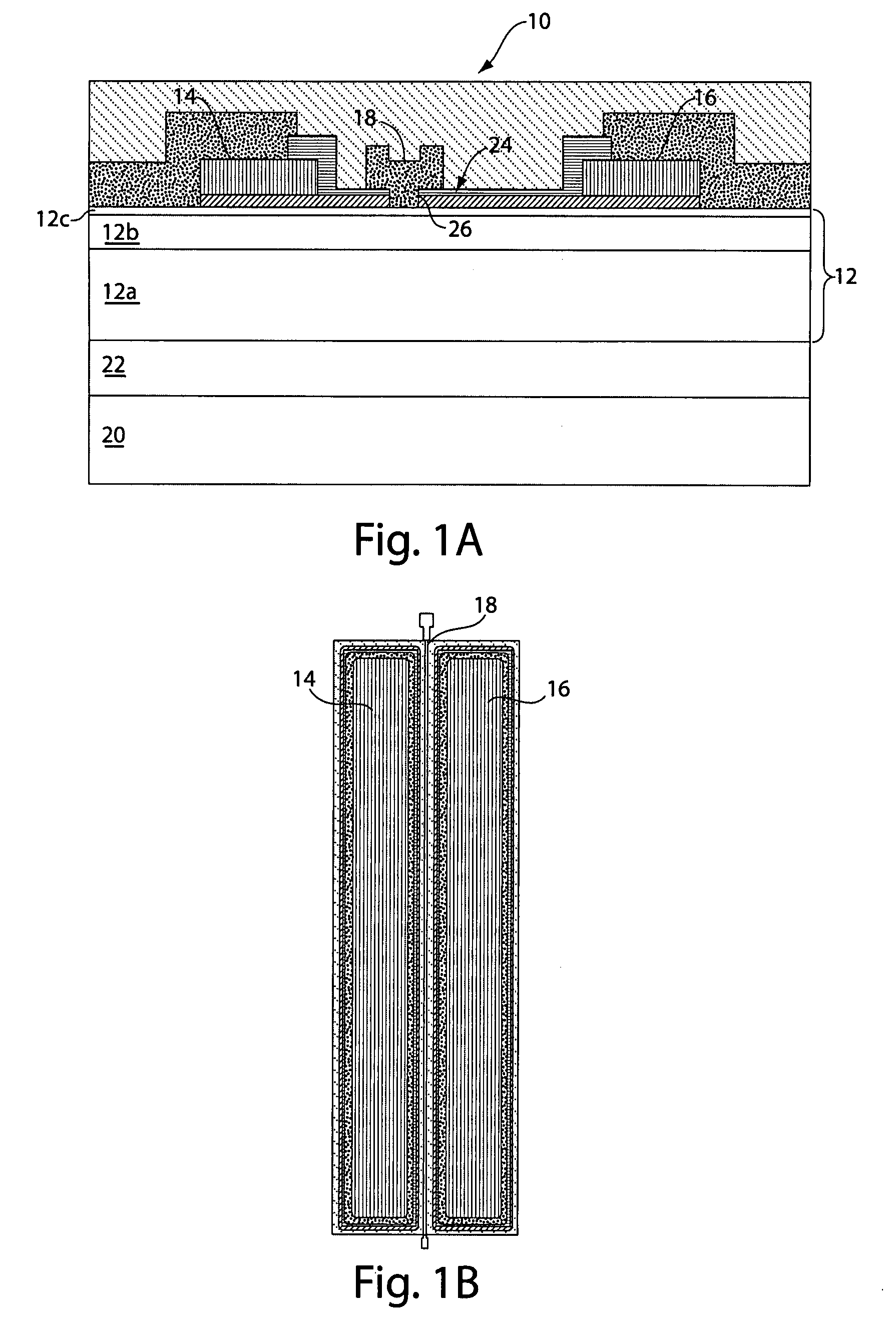
Gallium nitride material transistors and methods associated with the same
PatentInactiveUS20100019850A1
Innovation
- The development of gallium nitride material transistors with active regions formed in gallium nitride layers, integrated with a matching circuit to transform impedance, enabling the amplification of input signals to produce output signals with an adjacent channel power ratio (ACPR) of less than or equal to −20 dBc, while maintaining high drain efficiencies and output powers.
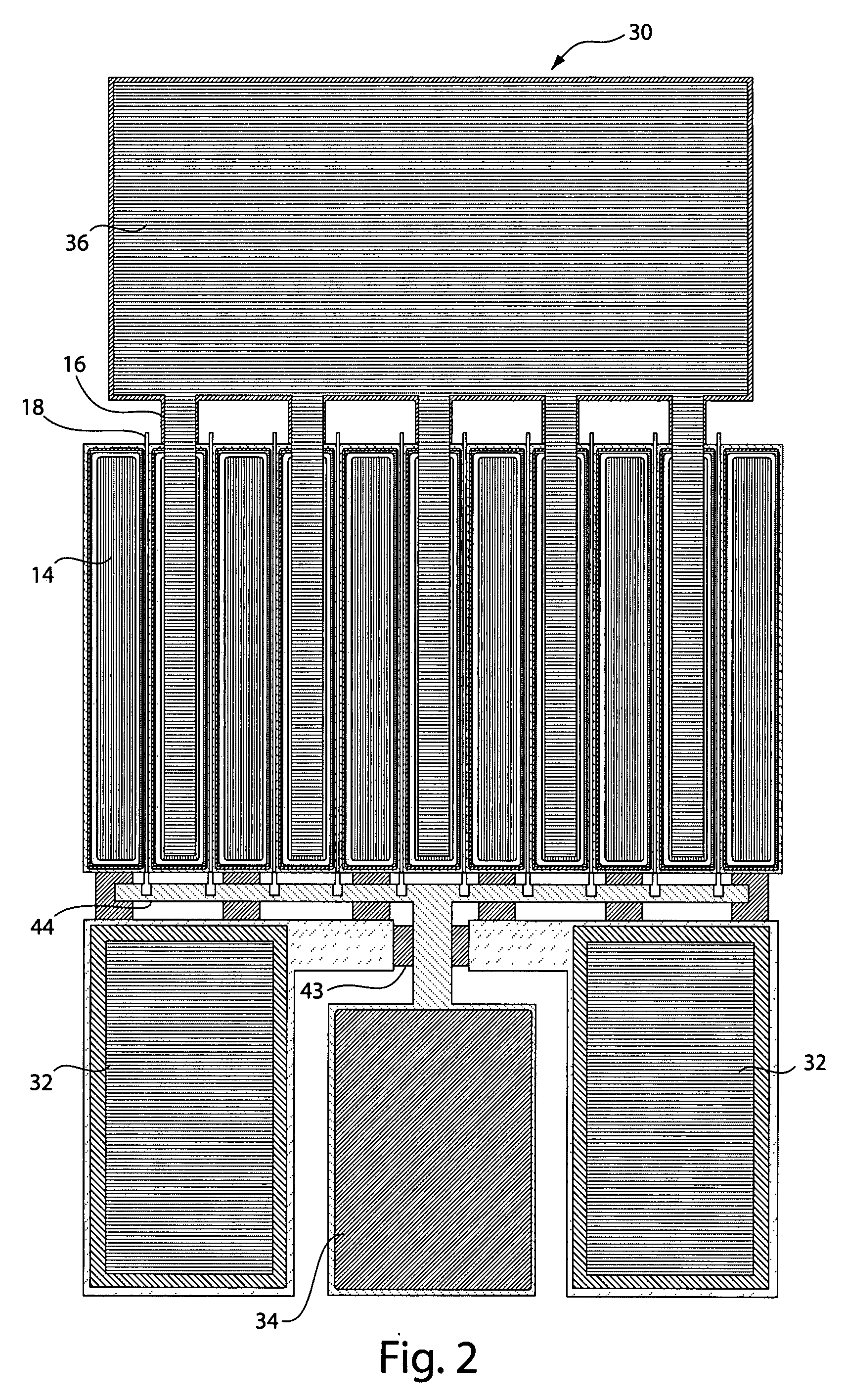
Gallium nitride material transistors and methods for wideband applications
PatentInactiveUS20070202360A1
Innovation
- The development of gallium nitride material transistors with active regions formed in gallium nitride layers, integrated with matching circuits to achieve low relative constellation error (RCE) values and high efficiency, enabling efficient signal amplification and transmission with excellent linearity and compliance with spectrum mask requirements.
Supply Chain Security for Defense GaN Components
The security of the Gallium Nitride (GaN) component supply chain represents a critical concern for defense applications, particularly as these advanced semiconductor materials become increasingly essential for next-generation military electronics. Defense systems rely on trusted component sources to ensure operational integrity and prevent potential vulnerabilities from compromised hardware. Currently, the GaN supply chain faces significant challenges related to geographic concentration, with a limited number of countries controlling key aspects of production.
The United States Department of Defense has identified GaN components as strategically important materials, implementing the Trusted Foundry Program to establish secure domestic manufacturing capabilities. Despite these efforts, approximately 65% of global GaN substrate production remains concentrated in Asia, creating potential bottlenecks and security vulnerabilities during geopolitical tensions or supply disruptions.
Verification and authentication protocols have emerged as essential safeguards within the defense GaN supply chain. These include advanced component tracking systems utilizing blockchain technology to create immutable records of component origins and handling. Additionally, non-destructive testing methodologies have been developed specifically for GaN devices to detect counterfeit or tampered components without compromising their functionality.
Risk assessment frameworks for GaN supply chains typically evaluate factors including geographic diversification of suppliers, transportation security measures, and cybersecurity protocols protecting manufacturing data. The Defense Microelectronics Activity (DMEA) has established a multi-tier supplier certification system that rates vendors based on security compliance, with only approximately 12% of global GaN suppliers currently meeting the highest security designation requirements.
Recent incidents have highlighted the vulnerability of specialized semiconductor supply chains. In 2021, three documented cases of counterfeit GaN components entering defense supply chains prompted enhanced screening protocols and supplier verification requirements. These incidents accelerated the development of quantum dot marking technologies that enable component-level authentication through unique, tamper-evident identifiers embedded during manufacturing.
Looking forward, emerging strategies for securing GaN supply chains include the development of domestic manufacturing capabilities through public-private partnerships, implementation of zero-trust verification frameworks throughout the component lifecycle, and international agreements establishing secure trade corridors for critical defense materials. The CHIPS Act provisions specifically targeting compound semiconductors represent a significant step toward addressing these security challenges.
Radiation Hardening of GaN Transistors
Radiation hardening of Gallium Nitride (GaN) transistors represents a critical advancement for defense electronics applications where exposure to ionizing radiation poses significant operational challenges. GaN devices inherently demonstrate superior radiation tolerance compared to silicon-based alternatives due to their wide bandgap properties and stronger atomic bonds, which reduce susceptibility to displacement damage and ionization effects.
Current radiation hardening techniques for GaN transistors follow two primary approaches: process-based hardening and design-based hardening. Process-based methods involve modifications to the semiconductor fabrication process, including specialized epitaxial layer structures, gate oxide engineering, and passivation techniques that minimize charge trapping. The introduction of buried p-type layers has shown particular promise in mitigating threshold voltage shifts under radiation exposure.
Design-based hardening implements circuit-level techniques such as redundancy, error correction, and specialized layout geometries that minimize charge collection areas. Enclosed-gate transistor layouts have demonstrated significant improvements in radiation tolerance by eliminating edge leakage paths commonly affected by radiation damage.
Recent testing protocols have established that GaN HEMTs (High Electron Mobility Transistors) can withstand total ionizing dose (TID) levels exceeding 1 Mrad(Si) while maintaining acceptable operational parameters. However, single-event effects (SEE) remain challenging, particularly single-event gate rupture (SEGR) which can cause catastrophic device failure in high-voltage applications.
The Defense Logistics Agency and Naval Research Laboratory have pioneered qualification standards specifically for radiation-hardened GaN devices, establishing test methodologies that evaluate performance under various radiation environments including gamma rays, neutrons, and heavy ions. These standards have evolved to address the unique failure mechanisms observed in GaN technology that differ significantly from silicon-based devices.
Emerging research focuses on novel buffer layer compositions and gate stack engineering to further enhance radiation tolerance. Aluminum nitride (AlN) interlayers and field plates have shown promising results in reducing electron trapping and improving device stability under radiation stress. Additionally, diamond-based heat spreading layers are being investigated to mitigate thermal issues that can exacerbate radiation damage effects.
The qualification of radiation-hardened GaN transistors requires comprehensive testing across temperature extremes (-55°C to 125°C) while simultaneously exposed to radiation, as performance degradation mechanisms often demonstrate synergistic effects between thermal and radiation stressors. This multi-stress testing approach has become standard practice for defense-grade GaN components intended for space, nuclear, and tactical military applications.
Unlock deeper insights with Patsnap Eureka Quick Research — get a full tech report to explore trends and direct your research. Try now!
Generate Your Research Report Instantly with AI Agent
Supercharge your innovation with Patsnap Eureka AI Agent Platform!
