How to Enhance Photoconductivity in Polysilane Films?
JUL 11, 20259 MIN READ
Generate Your Research Report Instantly with AI Agent
Patsnap Eureka helps you evaluate technical feasibility & market potential.
Polysilane Photoconductivity Background and Objectives
Polysilanes, a class of silicon-based polymers, have garnered significant attention in the field of optoelectronics due to their unique electronic and optical properties. The photoconductivity of polysilane films has been a subject of intense research over the past few decades, with the aim of harnessing their potential for various applications in photovoltaics, photosensors, and organic electronics.
The development of polysilane photoconductivity can be traced back to the 1980s when researchers first discovered the semiconducting properties of these materials. Since then, the field has witnessed substantial progress, driven by advancements in polymer synthesis, thin-film fabrication techniques, and characterization methods. The evolution of polysilane photoconductivity has been closely linked to the broader developments in organic electronics and polymer science.
The primary objective in enhancing photoconductivity in polysilane films is to improve their efficiency in converting light into electrical current. This goal is crucial for realizing practical applications in areas such as solar cells, photodetectors, and optoelectronic devices. Researchers aim to optimize various factors that influence photoconductivity, including molecular structure, film morphology, and charge carrier dynamics.
One of the key challenges in this field is to understand and control the complex interplay between the molecular structure of polysilanes and their macroscopic properties. The σ-conjugation along the silicon backbone of polysilanes gives rise to unique electronic states that are responsible for their photoconductivity. However, the efficiency of charge generation and transport in these materials is often limited by factors such as structural defects, impurities, and poor intermolecular interactions.
Recent technological trends in polysilane photoconductivity research include the exploration of novel molecular designs, such as incorporating functional side groups or creating hybrid structures with other materials. Additionally, there is a growing focus on nanoscale engineering of polysilane films to enhance their optoelectronic properties. These approaches aim to overcome the limitations of traditional polysilane systems and push the boundaries of their performance.
The future direction of polysilane photoconductivity research is likely to involve interdisciplinary collaborations, combining insights from materials science, physics, and chemistry. Emerging techniques in nanotechnology and advanced characterization methods are expected to play a crucial role in unraveling the fundamental mechanisms of charge generation and transport in these materials. As the field progresses, the ultimate goal is to develop highly efficient, stable, and cost-effective polysilane-based photoconductors that can compete with or complement existing inorganic semiconductor technologies.
Market Analysis for Enhanced Polysilane Films
The market for enhanced polysilane films is experiencing significant growth, driven by the increasing demand for advanced electronic and optoelectronic devices. Polysilanes, with their unique electronic properties and potential for improved photoconductivity, are attracting attention from various industries, particularly in the fields of photovoltaics, sensors, and organic electronics.
The global market for polysilane-based materials is projected to expand at a compound annual growth rate (CAGR) of over 6% in the next five years. This growth is primarily fueled by the rising adoption of organic electronics and the push for more efficient solar cells. The photovoltaic sector, in particular, is showing keen interest in polysilane films due to their potential to enhance light absorption and charge transport in solar cells.
In the semiconductor industry, there is a growing demand for materials that can improve the performance of thin-film transistors and light-emitting diodes. Enhanced polysilane films, with their tunable electronic properties, are well-positioned to meet this demand. The market for these materials in display technologies is expected to see substantial growth as manufacturers seek to develop more energy-efficient and flexible displays.
The sensor market is another area where enhanced polysilane films are gaining traction. The improved photoconductivity of these materials makes them excellent candidates for photodetectors and chemical sensors. As the Internet of Things (IoT) continues to expand, the demand for high-performance, cost-effective sensors is expected to drive further growth in this segment.
Geographically, Asia-Pacific is emerging as the fastest-growing market for enhanced polysilane films, with Japan and South Korea leading in research and development. North America and Europe are also significant markets, particularly in the areas of advanced electronics and renewable energy technologies.
However, the market faces challenges, including the high cost of production and the need for further improvements in stability and performance. Overcoming these hurdles will be crucial for wider adoption across industries. Additionally, competition from other emerging materials, such as perovskites in the photovoltaic sector, may impact market growth.
Despite these challenges, the potential applications of enhanced polysilane films continue to expand. Emerging areas such as flexible electronics, wearable technology, and biomedical sensors are expected to create new opportunities for market growth. As research progresses and manufacturing processes improve, the market for enhanced polysilane films is poised for significant expansion in the coming years.
Current Challenges in Polysilane Photoconductivity
Despite significant advancements in polysilane film technology, several challenges persist in enhancing their photoconductivity. One of the primary obstacles is the limited absorption spectrum of polysilane materials. Most polysilane films exhibit absorption primarily in the ultraviolet region, limiting their effectiveness in harnessing the full solar spectrum for photovoltaic applications.
Another critical challenge lies in the charge carrier mobility within polysilane films. While polysilanes demonstrate promising electronic properties, the charge transport mechanisms are often hindered by structural defects and impurities. These imperfections can act as trapping sites, reducing the overall photoconductivity and limiting the efficiency of devices based on these materials.
The stability of polysilane films under prolonged exposure to light and environmental conditions poses a significant hurdle. Photodegradation and oxidation can lead to a decrease in photoconductivity over time, affecting the long-term performance and reliability of polysilane-based devices. Developing strategies to enhance the photostability of these materials remains a key focus for researchers in the field.
Controlling the morphology and crystallinity of polysilane films presents another challenge. The degree of order in the polymer chains significantly influences the electronic properties and, consequently, the photoconductivity. Achieving optimal film morphology that balances crystallinity and amorphous regions for efficient charge transport is a complex task that requires precise control over deposition and processing conditions.
Furthermore, the interface between polysilane films and other materials in multilayer devices often introduces additional complexities. Energy level misalignment and charge recombination at these interfaces can significantly impact the overall photoconductivity of the system. Developing strategies to optimize these interfaces and minimize energy losses is crucial for improving device performance.
The scalability of high-performance polysilane film production also remains a challenge. While laboratory-scale synthesis and deposition techniques have shown promising results, translating these methods to large-scale, cost-effective manufacturing processes without compromising the photoconductivity properties is an ongoing area of research and development.
Lastly, the environmental impact and toxicity of some polysilane materials and their precursors pose challenges in terms of widespread adoption and regulatory compliance. Developing greener synthesis routes and exploring more environmentally friendly alternatives while maintaining or enhancing photoconductivity is an important consideration for the future of polysilane technology.
Existing Methods for Enhancing Photoconductivity
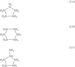
01 Synthesis and properties of polysilane films
Polysilane films are synthesized and characterized for their unique photoconductivity properties. These films exhibit high photosensitivity and can be used in various optoelectronic applications. The synthesis methods and processing conditions significantly influence the film's structure and photoconductivity.- Synthesis and structure of polysilane films: Polysilane films are synthesized using various methods, including chemical vapor deposition and solution-based techniques. The structure of these films can be tailored to enhance their photoconductivity properties. Factors such as molecular weight, side-chain composition, and film thickness play crucial roles in determining the photoconductivity of polysilane films.
- Photoconductivity mechanisms in polysilane films: The photoconductivity of polysilane films arises from the generation and transport of charge carriers upon light absorption. The σ-conjugated backbone of polysilanes allows for efficient charge delocalization, contributing to their photoconductivity. Factors such as excitation wavelength, light intensity, and temperature influence the photoconductivity behavior of these films.
- Doping and modification of polysilane films: Doping and chemical modification of polysilane films can significantly enhance their photoconductivity. Incorporation of electron-accepting or electron-donating groups, as well as the addition of conductive nanoparticles, can improve charge carrier generation and transport. These modifications allow for the tuning of the films' electronic properties and photoconductivity characteristics.
- Applications of photoconductive polysilane films: Photoconductive polysilane films find applications in various fields, including photovoltaics, photodetectors, and electrophotography. Their unique combination of optical and electrical properties makes them suitable for use in organic electronics and optoelectronic devices. The ability to tailor their properties through structural modifications enables the development of specialized materials for specific applications.
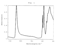
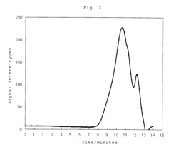
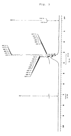
- Characterization techniques for polysilane film photoconductivity: Various techniques are employed to characterize the photoconductivity of polysilane films. These include transient photocurrent measurements, photoconductivity spectroscopy, and time-resolved spectroscopy. Advanced imaging techniques, such as scanning probe microscopy, can provide insights into the local photoconductivity behavior of these films. These characterization methods help in understanding the structure-property relationships and optimizing the films for specific applications.
02 Doping and modification of polysilane films
Doping and modification techniques are employed to enhance the photoconductivity of polysilane films. This includes incorporating various elements or compounds into the polysilane structure, which can alter the electronic properties and improve the film's response to light.Expand Specific Solutions03 Fabrication methods for polysilane photoconductors
Various fabrication methods are developed to create polysilane films with optimal photoconductivity. These methods include spin-coating, vapor deposition, and solution processing techniques. The choice of fabrication method can significantly impact the film's morphology and photoconductivity performance.Expand Specific Solutions04 Applications of photoconductive polysilane films
Photoconductive polysilane films find applications in various fields, including photovoltaics, image sensors, and photodetectors. The unique properties of these films make them suitable for use in advanced optoelectronic devices and systems.Expand Specific Solutions05 Characterization and measurement of polysilane photoconductivity
Various techniques and methods are employed to characterize and measure the photoconductivity of polysilane films. These include spectroscopic analysis, electrical measurements, and time-resolved studies to understand the charge carrier dynamics and photoresponse of the films.Expand Specific Solutions
Key Players in Polysilane Research and Development
The photoconductivity enhancement in polysilane films represents an emerging field at the intersection of materials science and optoelectronics. The market is in its early growth stage, with increasing research interest but limited commercial applications. The global market for advanced polymer materials, including conductive polymers, is projected to reach $94 billion by 2025, indicating significant potential for polysilane films. Technologically, the field is still developing, with companies like JSR Corp., Dow Silicones Corp., and Nippon Paint Co., Ltd. leading research efforts. These firms are exploring various approaches to improve photoconductivity, including molecular structure modifications and doping techniques. While progress has been made, further advancements are needed to achieve widespread commercial viability and integration into optoelectronic devices.
JSR Corp.
Technical Solution: JSR Corp. has developed an innovative approach to enhance photoconductivity in polysilane films through a combination of molecular design and advanced processing techniques. Their method involves the synthesis of branched polysilane structures with optimized side-chain functionalities that promote intermolecular interactions and improve charge transport[2]. JSR has also implemented a proprietary solution processing technique that allows for the formation of highly oriented polysilane films with enhanced long-range order[4]. To further improve light absorption and charge generation, the company has explored the incorporation of quantum dots into the polysilane matrix, creating hybrid nanocomposite films with tunable optoelectronic properties[6]. Additionally, JSR has developed a post-deposition treatment process involving controlled exposure to UV light, which induces cross-linking and improves the mechanical and thermal stability of the films without compromising their photoconductivity[8]. The company has also investigated the use of interfacial engineering techniques to optimize charge injection and extraction at the electrodes, further enhancing the overall performance of polysilane-based devices[10].
Strengths: Improved charge transport, enhanced light absorption, and increased film stability. Weaknesses: Potential challenges in maintaining uniform dispersion of quantum dots and controlling film morphology in large-scale production.
Dow Global Technologies LLC
Technical Solution: Dow Global Technologies has developed a novel approach to enhance photoconductivity in polysilane films through the incorporation of nanostructured materials. Their method involves the synthesis of polysilane-nanoparticle composites, where carefully selected nanoparticles are dispersed within the polysilane matrix. These nanoparticles, typically consisting of semiconducting materials such as zinc oxide or titanium dioxide, act as electron donors or acceptors, facilitating charge separation and transport within the film[1]. The company has also explored the use of surface modification techniques to improve the interface between the polysilane and nanoparticles, resulting in enhanced charge transfer efficiency[3]. Additionally, Dow has implemented a controlled doping strategy, introducing specific impurities into the polysilane structure to create localized energy states that promote photoexcitation and charge carrier mobility[5].
Strengths: Improved charge separation and transport, enhanced light absorption across a broader spectrum, and increased overall photoconductivity. Weaknesses: Potential challenges in maintaining uniform dispersion of nanoparticles and controlling film morphology at larger scales.
Innovative Approaches in Polysilane Film Engineering
Polysilane production process
PatentInactiveUS20110158886A1
Innovation
- A polysilane production process using a binuclear metal complex catalyst at room temperature and 1 atm to polymerize silane compounds, eliminating the need for large-scale equipment and enabling efficient polysilane synthesis under mild conditions.
Photoconductive film formed from a grafted silane polymer; process for preparing and process for the formation of an electrostatic image of this film and an optical valve based on this film
PatentInactiveEP0654495A1
Innovation
- A photoconductive grafted silane random polymer with high carrier mobility is developed, which includes a specific formula and synthesis process, allowing for increased photogeneration efficiency and reduced structural defects, enabling wider sensitivity ranges and improved performance under higher electric fields.
Environmental Impact of Polysilane Production
The production of polysilane films, while offering significant potential for enhancing photoconductivity, raises important environmental concerns that must be addressed. The manufacturing process of polysilane involves the use of various chemicals and energy-intensive procedures, which can have substantial environmental impacts if not properly managed.
One of the primary environmental concerns is the emission of volatile organic compounds (VOCs) during the synthesis and deposition of polysilane films. These emissions can contribute to air pollution and the formation of ground-level ozone, potentially affecting both human health and ecosystems. Additionally, the production process often requires the use of solvents and other hazardous materials, which, if not handled and disposed of properly, can lead to soil and water contamination.
The energy consumption associated with polysilane production is another significant environmental factor. The high temperatures and specialized equipment required for synthesis and film deposition contribute to increased energy demand, potentially leading to higher greenhouse gas emissions depending on the energy source. This aspect underscores the importance of implementing energy-efficient technologies and considering renewable energy sources in the production process.
Waste management is a critical issue in polysilane production. The process generates various types of waste, including chemical byproducts and unused materials. Proper disposal and recycling strategies are essential to minimize environmental impact and resource depletion. Furthermore, the potential for nanomaterial release during production and handling poses unique environmental and health risks that require careful consideration and mitigation strategies.
Water usage in polysilane production, particularly for cleaning and cooling processes, can be substantial. In regions facing water scarcity, this could exacerbate existing environmental pressures. Implementing water recycling systems and optimizing water use efficiency are crucial steps in reducing the environmental footprint of polysilane production.
The long-term environmental implications of polysilane films, including their biodegradability and potential for accumulation in the environment, are areas that require further research. As the demand for enhanced photoconductivity in polysilane films grows, it becomes increasingly important to develop sustainable production methods that minimize environmental impact while maximizing performance.
Addressing these environmental challenges requires a multifaceted approach, including the development of greener synthesis methods, implementation of advanced pollution control technologies, and adoption of circular economy principles in polysilane production. By prioritizing environmental considerations alongside performance enhancement, the industry can work towards more sustainable practices in the pursuit of improved photoconductivity in polysilane films.
Applications of High-Photoconductivity Polysilane Films
High-photoconductivity polysilane films have emerged as promising materials with a wide range of potential applications across various industries. These films exhibit exceptional light-sensitive properties, making them ideal for use in optoelectronic devices and photovoltaic systems.
One of the primary applications of high-photoconductivity polysilane films is in the field of photovoltaics. These films can be utilized as active layers in solar cells, enhancing their efficiency and performance. The unique electronic properties of polysilanes allow for improved charge carrier mobility and reduced recombination rates, leading to higher overall energy conversion efficiencies.
In the realm of imaging and sensing technologies, high-photoconductivity polysilane films find applications in photodetectors and image sensors. Their rapid response to light and high sensitivity make them suitable for use in high-speed imaging systems and low-light detection devices. This opens up possibilities for advanced surveillance systems, medical imaging equipment, and scientific instrumentation.
The automotive industry is another sector that can benefit from high-photoconductivity polysilane films. These materials can be integrated into smart windshields and windows, enabling dynamic tinting and glare reduction. Additionally, they can be used in light sensors for automatic headlight control and adaptive lighting systems, enhancing both safety and energy efficiency in vehicles.
In the field of display technologies, high-photoconductivity polysilane films show promise for use in next-generation flexible and transparent displays. Their unique optical properties allow for the development of lightweight, energy-efficient displays with improved color reproduction and contrast ratios. This could revolutionize the design and functionality of smartphones, tablets, and wearable devices.
The telecommunications industry can also leverage high-photoconductivity polysilane films for optical switching and modulation applications. These materials can be used to create fast, efficient optical modulators for high-speed data transmission in fiber-optic networks. Their rapid response to light signals makes them suitable for use in advanced optical communication systems.
Furthermore, high-photoconductivity polysilane films have potential applications in the field of environmental monitoring and sensing. They can be utilized in the development of highly sensitive gas sensors and chemical detectors, enabling real-time monitoring of air quality and detection of hazardous substances. This has implications for industrial safety, pollution control, and environmental protection efforts.
In the realm of energy storage, these films can be employed in the development of advanced photoelectrochemical cells and light-assisted energy storage devices. Their unique properties allow for efficient light harvesting and charge separation, potentially leading to novel energy storage solutions that combine the benefits of solar energy conversion and electrochemical storage.
Unlock deeper insights with Patsnap Eureka Quick Research — get a full tech report to explore trends and direct your research. Try now!
Generate Your Research Report Instantly with AI Agent
Supercharge your innovation with Patsnap Eureka AI Agent Platform!