

Polysilane Applications in Advanced Electronics: A Technical Overview
JUL 11, 20259 MIN READ
Generate Your Research Report Instantly with AI Agent
Patsnap Eureka helps you evaluate technical feasibility & market potential.
Polysilane Evolution and Objectives
Polysilanes, a class of silicon-based polymers, have undergone significant evolution since their discovery in the mid-20th century. Initially considered as mere curiosities in polymer chemistry, these materials have gradually emerged as promising candidates for advanced electronic applications. The journey of polysilanes from laboratory novelties to potential game-changers in electronics is marked by several key milestones and technological breakthroughs.
In the 1980s, researchers began to recognize the unique electronic properties of polysilanes, particularly their σ-conjugation along the silicon backbone. This discovery sparked intense interest in exploring their potential for semiconductor applications. The subsequent decades saw a steady progression in synthesis techniques, allowing for greater control over molecular weight, polydispersity, and side-group functionalization. These advancements laid the foundation for tailoring polysilanes to specific electronic requirements.
The turn of the millennium brought about a renewed focus on polysilanes as materials for organic electronics. Their high charge carrier mobility, coupled with solution processability, positioned them as attractive alternatives to traditional inorganic semiconductors. This period witnessed the development of polysilane-based thin-film transistors, photovoltaic cells, and light-emitting diodes, demonstrating their versatility in various electronic devices.
Recent years have seen a convergence of polysilane research with emerging fields such as flexible electronics and wearable technology. The inherent flexibility of these polymers, combined with their electronic properties, makes them ideal candidates for next-generation flexible displays, sensors, and electronic skins. Additionally, the integration of polysilanes with nanomaterials has opened up new avenues for hybrid electronic systems with enhanced performance characteristics.
Looking ahead, the objectives for polysilane research in advanced electronics are multifaceted. One primary goal is to further improve the charge transport properties of polysilanes, aiming to achieve mobilities comparable to or exceeding those of amorphous silicon. This would potentially enable their widespread adoption in high-performance electronic devices. Another critical objective is to enhance the environmental stability of polysilanes, addressing issues related to oxidation and degradation that have historically limited their practical applications.
Furthermore, researchers are focusing on developing novel polysilane architectures, such as hyperbranched and dendritic structures, to exploit unique three-dimensional electronic properties. The aim is to create materials with tailored band gaps and improved charge separation capabilities for more efficient optoelectronic devices. Concurrently, efforts are underway to scale up the production of high-quality polysilanes, making them economically viable for large-scale electronic manufacturing processes.
In conclusion, the evolution of polysilanes in advanced electronics reflects a journey of continuous innovation and discovery. From their humble beginnings to their current status as promising materials for next-generation electronics, polysilanes have demonstrated remarkable potential. The ongoing research objectives are poised to further unlock their capabilities, potentially revolutionizing the landscape of electronic materials and devices in the coming years.
Market Demand Analysis
The market demand for polysilane applications in advanced electronics has been steadily growing, driven by the increasing need for high-performance materials in various electronic devices and components. Polysilanes, with their unique electronic and optical properties, have garnered significant attention from both industry and academia.
In the semiconductor industry, polysilanes have shown promise as potential alternatives to traditional silicon-based materials. The demand for faster, smaller, and more energy-efficient electronic devices has pushed manufacturers to explore novel materials that can overcome the limitations of conventional silicon technology. Polysilanes, with their tunable bandgap and high electron mobility, offer potential solutions for next-generation transistors and memory devices.
The optoelectronics sector has also demonstrated a growing interest in polysilane-based materials. The photoluminescent properties of certain polysilanes make them attractive candidates for light-emitting diodes (LEDs) and organic light-emitting diodes (OLEDs). As the global demand for energy-efficient lighting and display technologies continues to rise, polysilanes are positioned to play a crucial role in meeting these market needs.
In the field of photovoltaics, polysilanes have shown potential as electron-transporting materials in solar cells. With the increasing focus on renewable energy sources and the push for more efficient solar technologies, the demand for advanced materials like polysilanes is expected to grow significantly in the coming years.
The emerging field of flexible electronics has also created new opportunities for polysilane applications. The ability to process polysilanes into thin films and their compatibility with various substrates make them suitable for use in flexible displays, wearable devices, and other bendable electronic components. As the market for flexible electronics expands, the demand for polysilane-based materials is likely to increase.
Furthermore, the growing interest in quantum computing and spintronics has opened up new avenues for polysilane applications. The unique electronic properties of polysilanes make them potential candidates for quantum bits (qubits) and spin-based devices, which could drive demand in these cutting-edge fields.
While the market for polysilane applications in advanced electronics is still relatively niche compared to traditional materials, industry analysts predict substantial growth in the coming years. The increasing research and development efforts, coupled with the potential for breakthrough applications, suggest a promising future for polysilanes in the electronics industry.
Technical Challenges
Polysilanes, despite their promising potential in advanced electronics, face several significant technical challenges that hinder their widespread adoption and commercialization. One of the primary obstacles is the inherent instability of these materials when exposed to light, heat, or oxygen. This photosensitivity, while beneficial in some applications, can lead to rapid degradation of the polymer structure, limiting the longevity and reliability of polysilane-based devices.
The synthesis of high-quality, uniform polysilanes remains a complex process. Current methods often result in polydisperse products with varying chain lengths and molecular weights, which can significantly impact the material's electronic properties. Achieving precise control over the molecular structure and composition of polysilanes is crucial for optimizing their performance in electronic applications.
Another major challenge lies in the integration of polysilanes with existing semiconductor technologies. The compatibility of these materials with conventional fabrication processes and device architectures is limited, requiring the development of new manufacturing techniques and device designs. This integration challenge extends to issues of adhesion, interface quality, and overall device stability when incorporating polysilanes into complex electronic systems.
The electrical properties of polysilanes, while promising, still fall short of the performance levels required for many advanced electronic applications. Improving charge carrier mobility, enhancing conductivity, and reducing charge trapping are critical areas that require further research and development. Additionally, the band gap engineering of polysilanes to tailor their electronic properties for specific applications remains a significant technical hurdle.
Environmental stability is another key concern. Many polysilanes are sensitive to moisture and atmospheric contaminants, which can rapidly degrade their performance. Developing effective encapsulation methods and improving the intrinsic stability of these materials without compromising their desirable properties is a complex challenge that researchers are actively addressing.
Scalability and cost-effectiveness in production represent further technical challenges. Current synthesis methods for high-quality polysilanes are often laboratory-scale processes that are difficult to scale up for industrial production. Developing economically viable, large-scale manufacturing processes while maintaining material quality and consistency is essential for the commercial viability of polysilane-based electronics.
Lastly, the long-term reliability and performance of polysilane-based devices under real-world operating conditions remain largely unknown. Comprehensive studies on the aging, degradation mechanisms, and lifetime performance of these materials in various electronic applications are necessary to build confidence in their use for commercial products.
Current Polysilane Solutions
01 Synthesis and properties of polysilanes
Polysilanes are synthesized through various methods and exhibit unique properties. These silicon-based polymers have applications in electronics, optics, and materials science due to their electronic and optical characteristics. The synthesis and modification of polysilanes can be tailored to achieve specific properties for different applications.- Synthesis and properties of polysilanes: Polysilanes are silicon-based polymers with a backbone consisting of silicon atoms. They can be synthesized through various methods and exhibit unique optical and electronic properties. These polymers have applications in photoresists, semiconductors, and optoelectronic devices due to their high thermal stability and conductivity.
- Polysilane-based coatings and films: Polysilanes can be used to create thin films and coatings with specific properties. These films can be applied to various substrates and may exhibit characteristics such as improved adhesion, chemical resistance, or optical properties. The process of forming these coatings often involves deposition techniques or curing methods to achieve desired film characteristics.
- Polysilane applications in photoresists: Polysilanes are utilized in photoresist formulations for semiconductor manufacturing. They can act as photosensitive materials or as additives to enhance the performance of photoresists. The incorporation of polysilanes can improve resolution, sensitivity, and pattern transfer in photolithography processes.
- Functionalization and modification of polysilanes: Polysilanes can be functionalized or modified to tailor their properties for specific applications. This may involve the introduction of various functional groups, copolymerization with other monomers, or post-polymerization modifications. These modifications can enhance the polymer's solubility, reactivity, or compatibility with other materials.
- Polysilane-based composites and hybrid materials: Polysilanes can be combined with other materials to create composites or hybrid materials with enhanced properties. These may include inorganic-organic hybrid materials, nanocomposites, or blends with other polymers. The resulting materials can exhibit improved mechanical, thermal, or electrical properties compared to the individual components.
02 Polysilanes in photoresist and lithography applications
Polysilanes are utilized in photoresist formulations and lithography processes. Their photosensitive nature and ability to form stable patterns make them suitable for use in semiconductor manufacturing and other microfabrication techniques. These materials can be optimized for improved resolution and sensitivity in lithographic processes.Expand Specific Solutions03 Polysilane-based thin films and coatings
Polysilanes can be used to create thin films and coatings with specific properties. These films find applications in various fields, including electronics, optics, and protective coatings. The deposition and processing of polysilane films can be controlled to achieve desired thickness, uniformity, and functional characteristics.Expand Specific Solutions04 Functionalization and modification of polysilanes
Polysilanes can be functionalized or modified to enhance their properties or introduce new functionalities. This includes the incorporation of various side groups, crosslinking agents, or other reactive moieties. Such modifications allow for the tailoring of polysilanes for specific applications or to improve their compatibility with other materials.Expand Specific Solutions05 Polysilanes in composite materials
Polysilanes can be incorporated into composite materials to impart unique properties or enhance existing characteristics. These composites may combine the benefits of polysilanes with other materials, such as organic polymers or inorganic compounds. The resulting composites can exhibit improved mechanical, thermal, or electrical properties for various applications.Expand Specific Solutions
Key Industry Players
The polysilane applications in advanced electronics market is in a growth phase, driven by increasing demand for high-performance electronic materials. The market size is expanding, with projections indicating significant growth potential in the coming years. Technologically, polysilanes are advancing rapidly, with companies like JSR Corp., Wacker Chemie AG, and Nissan Chemical Corp. leading innovation in synthesis methods and application development. These firms are focusing on improving polysilane properties for use in semiconductors, display technologies, and photoresists. While the technology is maturing, there is still room for breakthroughs in areas such as stability, processability, and integration into existing manufacturing processes. The competitive landscape is characterized by a mix of established chemical companies and specialized materials firms, with ongoing research collaborations between industry and academic institutions like the National University of Singapore driving further advancements.
JSR Corp.
Technical Solution: JSR Corporation has made significant advancements in polysilane applications for electronics, focusing on their use in photoresist materials for semiconductor manufacturing. Their polysilane-based photoresists offer high resolution and sensitivity, crucial for producing advanced microchips with smaller feature sizes[10]. JSR has developed proprietary polysilane synthesis methods that allow for precise control of molecular weight and side-group functionalization, enabling tailored properties for specific electronic applications[11]. The company has also explored the use of polysilanes in organic thin-film transistors, leveraging their unique electronic properties to create high-performance, solution-processable semiconducting materials[12]. Additionally, JSR is investigating polysilanes as precursors for silicon carbide materials, which have applications in power electronics and high-temperature sensors.
Strengths: Expertise in photoresist technology and integration with semiconductor manufacturing processes. Ability to tailor polysilane properties for specific applications. Weaknesses: May face competition from alternative photoresist materials and emerging lithography technologies.
Wacker Chemie AG
Technical Solution: Wacker Chemie AG has developed advanced polysilane materials for electronics applications. Their SILRES® polysilane resins offer excellent thermal stability and electrical insulation properties[1]. These materials are used in the production of thin-film transistors for flexible displays and photovoltaic cells. Wacker's polysilanes feature controlled molecular weight distribution and high purity, enabling precise control of film thickness and uniformity in electronic device fabrication[2]. The company has also explored the use of polysilanes as precursors for silicon carbide ceramics, which have applications in high-temperature electronics and power devices[3].
Strengths: High purity and controlled properties for precise electronic applications. Versatility in both organic electronics and ceramic precursors. Weaknesses: May face competition from alternative materials like metal oxides in some applications.
Core Polysilane Innovations
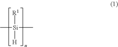
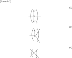
Polysilane and polysilane-containing resin composition
PatentInactiveUS8163863B2
Innovation
- Introducing a Si—H group into the polysilane main chain and bonding a hydrosilylatable compound with functional groups like hydroxyl, carboxyl, or epoxy groups, allowing for controlled hydrosilylation to enhance solubility and reactivity without complex steps or special apparatus.


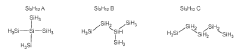
Process for producing liquid polysilanes and isomer enriched higher silanes
PatentWO2020077183A1
Innovation
- The synthesis of higher silanes involves catalytic transformation of lower silanes using heterogeneous catalysts, such as Group I, II, or III element-based catalysts, to control temperature, residence time, and reactant ratios, resulting in isomerically enriched polysilanes with specific isomer ratios and high purity.
Environmental Impact Assessment
The environmental impact of polysilane applications in advanced electronics is a critical consideration as this technology continues to evolve. Polysilanes, being silicon-based polymers, offer unique properties that make them attractive for various electronic applications. However, their production, use, and disposal can have significant environmental implications.
The manufacturing process of polysilanes often involves the use of chlorosilanes and other potentially hazardous chemicals. These substances can pose risks to air and water quality if not properly managed. Emissions from production facilities may contribute to air pollution, while improper disposal of waste materials could lead to soil and groundwater contamination.
In terms of energy consumption, the synthesis of polysilanes typically requires high temperatures and pressures, resulting in substantial energy use. This energy-intensive process contributes to the overall carbon footprint of polysilane-based electronic devices. However, it's worth noting that the potential energy efficiency gains in the final products may offset some of these environmental costs over the long term.
The use phase of polysilane-based electronics presents both challenges and opportunities from an environmental perspective. On one hand, these materials can enhance the performance and longevity of electronic devices, potentially reducing e-waste. On the other hand, the unique properties of polysilanes may complicate recycling processes, as they may not be compatible with existing recycling infrastructure for conventional electronics.
End-of-life considerations for polysilane-containing electronics are particularly important. The decomposition of polysilanes in landfills or through incineration could release silicon-based compounds into the environment. While silicon is generally considered non-toxic, the long-term effects of these decomposition products on ecosystems are not yet fully understood and require further research.
From a lifecycle assessment standpoint, the environmental impact of polysilanes in electronics must be evaluated holistically. This includes considering raw material extraction, manufacturing processes, energy consumption during use, and end-of-life management. Comparative studies with traditional electronic materials are necessary to determine whether polysilanes offer a net environmental benefit.
Efforts to mitigate the environmental impact of polysilanes in electronics are ongoing. These include developing greener synthesis methods, improving energy efficiency in manufacturing, and exploring bio-based alternatives. Additionally, research into effective recycling and safe disposal methods for polysilane-containing electronics is crucial for minimizing their environmental footprint.
Intellectual Property Landscape
The intellectual property landscape surrounding polysilane applications in advanced electronics is characterized by a complex network of patents and proprietary technologies. Major electronics companies and research institutions have been actively filing patents related to polysilane synthesis, processing, and integration into electronic devices.
One of the key areas of patent activity is in the development of novel polysilane structures and compositions. These patents often focus on improving the electrical and optical properties of polysilanes, making them more suitable for specific electronic applications. For instance, several patents describe methods for synthesizing polysilanes with controlled molecular weight and polydispersity, which are crucial factors in determining their performance in electronic devices.
Another significant area of intellectual property is centered on the integration of polysilanes into various electronic components. Patents in this category cover techniques for incorporating polysilanes into transistors, photoresistors, and other semiconductor devices. Many of these patents describe innovative fabrication processes that enable the seamless integration of polysilanes with traditional silicon-based electronics.
The use of polysilanes in optoelectronic applications has also generated substantial patent activity. These patents often relate to the development of polysilane-based light-emitting diodes (LEDs), photodetectors, and optical waveguides. The unique optical properties of polysilanes, such as their tunable bandgap and high photosensitivity, are frequently highlighted in these patents as key advantages over conventional materials.
In recent years, there has been a noticeable increase in patents related to the application of polysilanes in flexible and wearable electronics. These patents typically describe methods for depositing polysilane thin films on flexible substrates and techniques for enhancing their mechanical durability while maintaining their electronic properties.
The geographical distribution of polysilane-related patents reveals that Japan, the United States, and South Korea are leading in terms of patent filings. However, there is also significant activity from research institutions and companies in Europe and China, indicating a global interest in this technology.
It's worth noting that many of the key patents in this field are approaching their expiration dates, which could potentially lead to increased innovation and commercialization opportunities in the coming years. This evolving intellectual property landscape suggests that polysilanes are poised to play an increasingly important role in the development of next-generation electronic devices.
Unlock deeper insights with Patsnap Eureka Quick Research — get a full tech report to explore trends and direct your research. Try now!
Generate Your Research Report Instantly with AI Agent
Supercharge your innovation with Patsnap Eureka AI Agent Platform!