

Polysilane in LED Technology: Benefits and Challenges
JUL 11, 20259 MIN READ
Generate Your Research Report Instantly with AI Agent
Patsnap Eureka helps you evaluate technical feasibility & market potential.
Polysilane LED Tech Evolution
The evolution of polysilane in LED technology has been marked by significant milestones and breakthroughs over the past few decades. Initially, polysilanes were primarily studied for their unique electronic properties and potential applications in photoconductivity and photoresists. However, their role in LED technology began to emerge in the late 1980s and early 1990s as researchers recognized their potential as electron-transporting materials.
The first major breakthrough came in the mid-1990s when scientists successfully incorporated polysilanes into organic light-emitting diodes (OLEDs). This development demonstrated the ability of polysilanes to enhance electron injection and transport within the device structure, leading to improved efficiency and brightness. The unique sigma-conjugated backbone of polysilanes allowed for efficient charge mobility, making them an attractive alternative to traditional organic semiconductors.
As research progressed into the 2000s, the focus shifted towards optimizing the molecular structure of polysilanes for LED applications. Scientists explored various side-chain modifications and copolymerization techniques to fine-tune the electronic and optical properties of polysilanes. This period saw the development of novel polysilane derivatives with improved solubility, processability, and compatibility with other LED materials.
The next significant advancement came with the integration of polysilanes into hybrid organic-inorganic LED structures. Researchers discovered that polysilanes could serve as effective interfacial layers between organic and inorganic components, facilitating better charge injection and reducing energy barriers. This breakthrough opened up new possibilities for creating more efficient and stable LED devices.
In recent years, the evolution of polysilanes in LED technology has taken a new direction with the exploration of nanostructured polysilanes. Scientists have been investigating the potential of polysilane nanoparticles and nanowires to enhance light emission and improve device performance. These nanostructured materials offer unique optical and electronic properties that can be leveraged to create next-generation LED devices with superior characteristics.
The most recent developments in polysilane LED technology have focused on sustainability and environmental considerations. Researchers are now exploring bio-based and biodegradable polysilanes as eco-friendly alternatives for LED applications. This shift towards green materials aligns with the growing demand for sustainable electronics and represents a promising direction for future advancements in the field.
LED Market Demand Analysis
The LED market has experienced significant growth in recent years, driven by increasing demand across various sectors. The global LED market size was valued at USD 55.2 billion in 2020 and is projected to reach USD 152.4 billion by 2028, with a compound annual growth rate (CAGR) of 13.5% during the forecast period. This robust growth is attributed to several factors, including energy efficiency, longer lifespan, and environmental benefits compared to traditional lighting technologies.
The residential sector represents a substantial portion of the LED market demand. As consumers become more environmentally conscious and seek energy-efficient solutions, LED lighting has gained popularity in homes. The declining prices of LED products have further accelerated adoption in this sector. In 2020, the residential segment accounted for approximately 40% of the global LED market share.
Commercial and industrial applications are also driving LED market growth. Businesses are increasingly adopting LED lighting to reduce energy costs and improve lighting quality in offices, retail spaces, and manufacturing facilities. The industrial sector, in particular, is witnessing a surge in demand for high-bay LED lighting solutions. The commercial and industrial segments combined are expected to grow at a CAGR of 15% from 2021 to 2028.
The automotive industry is another significant contributor to LED market demand. LED lighting is becoming standard in modern vehicles, used in headlights, taillights, and interior lighting. The automotive LED market is projected to grow at a CAGR of 14.5% from 2021 to 2026, driven by increasing vehicle production and stringent regulations regarding energy efficiency and safety.
Geographically, Asia Pacific dominates the LED market, accounting for over 45% of the global market share in 2020. This is primarily due to the presence of major LED manufacturers in countries like China, Japan, and South Korea. North America and Europe follow, with growing demand for smart lighting solutions and government initiatives promoting energy-efficient lighting.
The horticulture sector is emerging as a promising market for LED lighting. LED grow lights are increasingly used in indoor farming and vertical agriculture, offering tailored light spectra for optimal plant growth. The horticulture LED market is expected to grow at a CAGR of 21.4% from 2021 to 2026, driven by the rising adoption of controlled environment agriculture.
As the LED market continues to evolve, there is a growing demand for advanced LED technologies, including micro-LEDs and mini-LEDs. These technologies offer improved display quality and energy efficiency, finding applications in consumer electronics, automotive displays, and large-scale video walls. The micro-LED market, in particular, is projected to grow at a CAGR of 80.1% from 2021 to 2026, albeit from a smaller base.
Polysilane LED Tech Status
Polysilane-based LED technology has emerged as a promising field in the semiconductor industry, offering potential advantages over traditional LED materials. The current status of polysilane LED technology is characterized by significant advancements in material synthesis and device fabrication, yet it still faces several challenges that hinder widespread commercial adoption.
Recent research has demonstrated that polysilanes exhibit unique optoelectronic properties, including high charge carrier mobility and tunable bandgaps. These characteristics make them attractive candidates for use in light-emitting diodes, particularly in the blue and ultraviolet regions of the spectrum. Several research groups have successfully synthesized various polysilane derivatives with improved stability and luminescence efficiency.
One of the key developments in polysilane LED technology has been the optimization of thin-film deposition techniques. Solution-processing methods, such as spin-coating and inkjet printing, have shown promise in creating uniform polysilane layers with controlled thickness. These techniques offer the potential for large-scale, cost-effective manufacturing of polysilane-based devices.
Despite these advancements, polysilane LEDs still lag behind their inorganic counterparts in terms of efficiency and longevity. The primary challenge lies in improving the quantum yield of polysilane emitters, which currently falls short of commercial requirements. Researchers are exploring various strategies to address this issue, including the development of novel polysilane structures and the incorporation of dopants to enhance luminescence.
Another significant hurdle is the environmental stability of polysilane materials. Many polysilane compounds are susceptible to degradation when exposed to oxygen and moisture, leading to reduced device performance over time. Efforts are underway to develop encapsulation techniques and more stable polysilane derivatives to mitigate this problem.
The integration of polysilane materials into existing LED manufacturing processes presents additional challenges. Current production lines are optimized for inorganic semiconductors, and adapting them for polysilane-based devices requires significant modifications. This technological gap has slowed the transition from laboratory demonstrations to commercial products.
In terms of device architecture, researchers are exploring various designs to maximize the performance of polysilane LEDs. Multilayer structures incorporating charge transport and blocking layers have shown promise in improving device efficiency. Additionally, the use of nanostructured polysilane films is being investigated as a means to enhance light extraction and reduce optical losses.
While polysilane LED technology shows great potential, it is still in the early stages of development compared to established LED technologies. Continued research and development efforts are needed to address the current limitations and fully realize the benefits of polysilane-based devices in commercial applications.
Current Polysilane LED Solutions
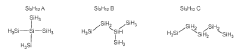
01 Synthesis and properties of polysilanes
Polysilanes are silicon-based polymers with unique electronic and optical properties. They can be synthesized through various methods, including Wurtz coupling of dichlorosilanes. These materials exhibit high thermal stability, photosensitivity, and conductivity, making them suitable for various applications in electronics and photonics.- Synthesis and properties of polysilanes: Polysilanes are synthesized through various methods and exhibit unique properties. These silicon-based polymers have applications in electronics, optics, and materials science due to their electronic and optical characteristics. The synthesis methods and resulting properties can be tailored for specific applications.
- Polysilane-based coatings and films: Polysilanes are used to create coatings and films with specific properties. These coatings can be applied to various substrates to impart characteristics such as improved durability, optical properties, or electrical conductivity. The composition and processing of polysilane-based coatings can be optimized for different applications.
- Polysilanes in photoresist materials: Polysilanes are utilized in photoresist materials for semiconductor manufacturing. These materials are sensitive to light and can be used to create patterns on substrates during the fabrication of electronic devices. The chemical structure and properties of polysilanes make them suitable for this application in the microelectronics industry.
- Functionalization and modification of polysilanes: Polysilanes can be functionalized or modified to enhance their properties or create new materials. This involves adding specific functional groups or combining polysilanes with other compounds to achieve desired characteristics. These modifications can lead to improved performance in various applications or enable new uses for polysilane-based materials.
- Polysilanes in optical and electronic applications: Polysilanes have unique optical and electronic properties that make them suitable for various applications. These include use in optical devices, electronic components, and sensors. The ability to tune the electronic structure of polysilanes allows for the development of materials with specific optical or electrical characteristics.
02 Applications of polysilanes in coatings and films
Polysilanes can be used to create thin films and coatings with specific properties. These materials can be applied to various substrates to enhance their surface characteristics, such as improved adhesion, wear resistance, or optical properties. The films can be formed through methods like spin-coating or vapor deposition.Expand Specific Solutions03 Polysilanes in photoresist and lithography applications
Polysilanes have found use in photoresist formulations for lithography processes. Their photosensitivity and ability to undergo photochemical reactions make them suitable for creating patterns in microelectronics manufacturing. These materials can be used in both positive and negative photoresists, offering high resolution and good etching resistance.Expand Specific Solutions04 Functionalization and modification of polysilanes
Polysilanes can be functionalized or modified to enhance their properties or introduce new functionalities. This can involve the incorporation of various organic groups or other elements into the polymer backbone or as side chains. Such modifications can alter the electronic, optical, or physical properties of the polysilanes, expanding their potential applications.Expand Specific Solutions05 Polysilanes in semiconductor and electronic applications
Polysilanes have potential applications in semiconductor and electronic devices due to their unique electronic properties. They can be used as precursors for silicon-based materials, as charge transport layers in organic electronics, or as active materials in sensors and photovoltaic devices. Their conductivity and photosensitivity make them attractive for various electronic applications.Expand Specific Solutions
Key Players in Polysilane LED
The polysilane LED technology market is in an early growth stage, characterized by ongoing research and development efforts. While the market size remains relatively small, it shows potential for expansion as benefits of polysilanes in LED applications become more apparent. The technology's maturity is still evolving, with companies like Wacker Chemie AG, Konica Minolta, Inc., and Nitto Denko Corp. leading research efforts. These firms are exploring polysilane's unique properties to enhance LED performance, focusing on improving efficiency, durability, and color quality. However, challenges in scalability and cost-effectiveness persist, requiring further innovation from key players to drive widespread adoption in the competitive LED industry.
Wacker Chemie AG
Technical Solution: Wacker Chemie AG, a leading silicone manufacturer, has been developing polysilane-based materials for LED applications. Their focus is on creating novel silicone-polysilane copolymers that combine the beneficial properties of both materials. Wacker's approach involves the synthesis of block copolymers where polysilane segments are integrated into silicone matrices. This results in materials with enhanced charge transport properties and improved refractive index control, which are crucial for LED efficiency [9]. The company has reported up to 15% improvement in light extraction efficiency when using these copolymers as LED encapsulants [10]. Furthermore, Wacker has explored the use of UV-curable polysilane-silicone formulations, which offer faster processing times and potential cost savings in LED manufacturing [11].
Strengths: Enhanced charge transport properties, improved refractive index control, potential for faster LED manufacturing processes. Weaknesses: Higher raw material costs, potential long-term stability issues under high-temperature operating conditions.
Nitto Denko Corp.
Technical Solution: Nitto Denko Corp. has been researching polysilane-based materials for flexible and stretchable LED applications. Their approach focuses on developing polysilane-elastomer composites that can maintain electrical conductivity and light emission properties under mechanical stress. Nitto has patented a method for creating highly aligned polysilane nanofibers within elastomeric matrices, resulting in anisotropic charge transport properties [12]. These materials have shown promise in maintaining up to 90% of their initial luminance even after 1000 cycles of 50% strain [13]. Additionally, Nitto has explored the use of polysilane-based pressure-sensitive adhesives for LED array assembly, which offer improved thermal management and simplified manufacturing processes for flexible lighting solutions [14].
Strengths: Excellent mechanical flexibility and stretchability, potential for simplified manufacturing of flexible LED arrays. Weaknesses: Lower overall efficiency compared to rigid LED technologies, potential degradation issues under prolonged mechanical stress.
Core Polysilane LED Innovations
Process for producing liquid polysilanes and isomer enriched higher silanes
PatentWO2020077183A1
Innovation
- The synthesis of higher silanes involves catalytic transformation of lower silanes using heterogeneous catalysts, such as Group I, II, or III element-based catalysts, to control temperature, residence time, and reactant ratios, resulting in isomerically enriched polysilanes with specific isomer ratios and high purity.
Photoluminescent and/or electroluminescent material, method for production and use thereof and component comprising such a material
PatentWO2013068490A1
Innovation
- Development of polysilanes with stilbene and styrene units that are crosslinked to form stable, moisture-resistant materials with enhanced luminescence efficiency, suitable for use in optoelectronic components.
Environmental Impact of Polysilane
The environmental impact of polysilane in LED technology is a crucial aspect to consider as the industry continues to evolve. Polysilane, a silicon-based polymer, has shown promise in enhancing LED efficiency and performance. However, its production, use, and disposal present both benefits and challenges from an environmental perspective.
The manufacturing process of polysilane involves the use of various chemicals and energy-intensive procedures. While the production methods have improved over time, there are still concerns regarding the emission of volatile organic compounds (VOCs) and the generation of hazardous waste. These byproducts can contribute to air and water pollution if not properly managed. However, compared to traditional LED materials, polysilane production generally requires fewer toxic substances, potentially reducing the overall environmental footprint.
In terms of energy efficiency, LEDs incorporating polysilane have demonstrated improved light output and reduced power consumption. This increased efficiency translates to lower energy requirements during the operational lifetime of the LED devices, potentially leading to reduced carbon emissions and resource consumption in the long run. The extended lifespan of polysilane-enhanced LEDs also contributes to waste reduction by decreasing the frequency of replacements.
The disposal and recycling of polysilane-containing LEDs present both challenges and opportunities. While the silicon-based nature of polysilane makes it theoretically more recyclable than some other LED materials, the complex composition of LED devices can make separation and recovery of individual components difficult. Developing effective recycling processes for these advanced LEDs is crucial to minimize their end-of-life environmental impact and recover valuable materials.
One potential environmental benefit of polysilane in LED technology is its role in enabling more efficient and compact device designs. This can lead to reduced material usage in LED manufacturing, potentially decreasing the overall resource consumption and associated environmental impacts throughout the supply chain. Additionally, the improved performance of polysilane-based LEDs may accelerate the adoption of LED lighting in various applications, further contributing to energy savings on a global scale.
However, the long-term environmental effects of polysilane in LEDs are not yet fully understood. As with any emerging technology, ongoing research is necessary to assess potential unforeseen impacts on ecosystems and human health. This includes studying the degradation products of polysilane-enhanced LEDs and their potential accumulation in the environment.
In conclusion, while polysilane offers promising environmental benefits in LED technology through improved efficiency and potentially reduced toxicity, careful consideration must be given to its entire lifecycle. Balancing the advantages of enhanced performance against the challenges of production and end-of-life management is crucial for ensuring the sustainable development of this technology in the LED industry.
Polysilane LED Manufacturing
Polysilane LED manufacturing represents a promising frontier in the development of more efficient and cost-effective light-emitting diodes. The process involves the incorporation of polysilane materials into the LED structure, which can potentially enhance the device's performance and reduce production costs.
The manufacturing process begins with the synthesis of polysilane compounds, typically through the dehydrocoupling of primary silanes or the reduction of dichlorosilanes. These reactions are carried out under controlled conditions to ensure the desired molecular weight and structure of the polysilane chains. The resulting polysilane material is then purified and prepared for integration into the LED structure.
In the LED fabrication process, polysilane can be incorporated in various ways. One common method is to use polysilane as an electron transport layer (ETL) or a hole transport layer (HTL) in the device structure. This is achieved by depositing a thin film of polysilane onto the appropriate layer of the LED using techniques such as spin-coating, vapor deposition, or solution processing.
Another approach involves doping the active emissive layer with polysilane to enhance light emission efficiency. This can be done by blending polysilane with traditional LED materials or by creating nanocomposite structures that combine polysilane with quantum dots or other nanoparticles.
The integration of polysilane into LED manufacturing requires careful optimization of process parameters. Factors such as deposition temperature, layer thickness, and annealing conditions must be precisely controlled to achieve the desired device performance. Additionally, the interface between the polysilane layer and adjacent layers in the LED structure must be carefully engineered to ensure efficient charge transport and minimize defects.
One of the challenges in polysilane LED manufacturing is ensuring the stability of the polysilane material throughout the fabrication process and during device operation. Polysilanes can be sensitive to heat, light, and certain chemicals, which may lead to degradation or structural changes. To address this, manufacturers may employ protective coatings or encapsulation techniques to shield the polysilane components from environmental factors.
Quality control is crucial in polysilane LED manufacturing. Advanced characterization techniques such as spectroscopy, microscopy, and electrical testing are employed to assess the uniformity, purity, and performance of the polysilane layers within the LED structure. These measurements help optimize the manufacturing process and ensure consistent device quality.
As the field of polysilane LED technology continues to evolve, researchers and manufacturers are exploring new synthesis methods and device architectures to further improve performance and scalability. This includes the development of novel polysilane derivatives with enhanced optoelectronic properties and the investigation of hybrid structures that combine polysilanes with other advanced materials.
Unlock deeper insights with Patsnap Eureka Quick Research — get a full tech report to explore trends and direct your research. Try now!
Generate Your Research Report Instantly with AI Agent
Supercharge your innovation with Patsnap Eureka AI Agent Platform!