

How to Select Material Composition for P–N Junctions
SEP 5, 20259 MIN READ
Generate Your Research Report Instantly with AI Agent
PatSnap Eureka helps you evaluate technical feasibility & market potential.
P-N Junction Materials Background and Objectives
P-N junctions represent one of the most fundamental building blocks in semiconductor technology, serving as the cornerstone for numerous electronic devices including diodes, transistors, solar cells, and integrated circuits. The historical development of P-N junction technology can be traced back to the 1940s, with significant advancements occurring through subsequent decades as semiconductor physics matured. The evolution of material selection for these junctions has progressed from elementary germanium and silicon to complex compound semiconductors and heterojunctions, reflecting the industry's continuous pursuit of enhanced performance characteristics.
The material composition of P-N junctions critically determines their electrical, optical, and thermal properties, directly influencing device efficiency, reliability, and application scope. Contemporary research focuses on optimizing these material selections to meet increasingly demanding requirements across diverse technological domains, from high-power electronics to ultra-sensitive photonics applications.
Current technological trends indicate a shift toward wider bandgap semiconductors, two-dimensional materials, and engineered heterojunctions that offer superior performance metrics compared to traditional silicon-based junctions. These advanced materials enable operation at higher temperatures, frequencies, and power densities while potentially reducing energy consumption—attributes essential for next-generation electronic systems.
The primary objectives of material selection for P-N junctions encompass several dimensions: enhancing carrier mobility and concentration to improve conductivity characteristics; optimizing bandgap properties to achieve desired optical and electrical responses; ensuring thermal stability for reliable operation across varying environmental conditions; and maintaining compatibility with existing fabrication processes to facilitate commercial viability and scalability.
Additionally, emerging applications in quantum computing, neuromorphic systems, and flexible electronics are driving research toward novel material combinations that exhibit unique quantum mechanical properties or mechanical flexibility while maintaining essential P-N junction functionality. These frontier applications necessitate innovative approaches to material engineering at atomic and molecular scales.
This technical exploration aims to comprehensively examine the principles, methodologies, and criteria governing material composition selection for P-N junctions, with particular emphasis on establishing systematic frameworks that can guide researchers and engineers through the complex decision-making process. By understanding the fundamental relationships between material properties and junction performance, we can develop more efficient, reliable, and application-specific semiconductor devices to address evolving technological challenges.
Market Applications and Demand Analysis
The P-N junction market has experienced significant growth driven by the expanding semiconductor industry, which reached approximately $573 billion in 2022. This fundamental building block of semiconductor devices continues to see increasing demand across multiple sectors, with particularly strong growth in power electronics, renewable energy systems, and advanced computing applications.
The automotive industry represents one of the fastest-growing markets for P-N junction technology, particularly with the electric vehicle revolution. The need for high-performance power semiconductors with optimized P-N junctions for inverters, converters, and battery management systems has created substantial demand for precisely engineered junction materials. Silicon carbide (SiC) and gallium nitride (GaN) P-N junctions are experiencing annual growth rates exceeding 25% in this sector due to their superior performance in high-temperature and high-voltage applications.
Renewable energy systems constitute another major market driver, with solar photovoltaics requiring highly efficient P-N junctions to maximize energy conversion. The global solar capacity additions reached 239 GW in 2022, creating sustained demand for advanced junction materials that can improve efficiency beyond the current commercial average of 20-22%. Multi-junction solar cells utilizing carefully selected material compositions can achieve efficiencies approaching 40%, representing a premium market segment.
The telecommunications sector, particularly with 5G infrastructure deployment, has created significant demand for high-frequency semiconductor devices with specialized P-N junction requirements. RF power amplifiers and other communication components benefit from materials like gallium arsenide (GaAs) and indium phosphide (InP) that offer superior electron mobility and frequency response characteristics.
Consumer electronics continue to drive volume demand for conventional silicon-based P-N junctions, but with increasing requirements for miniaturization and energy efficiency. The smartphone market alone, with annual shipments exceeding 1.2 billion units, creates massive demand for optimized junction technologies in processors, memory, and sensor applications.
Medical electronics represent an emerging high-value market segment, with imaging systems, implantable devices, and diagnostic equipment requiring specialized P-N junctions that can operate reliably in sensitive environments. This sector values material compositions that offer biocompatibility, radiation hardness, and ultra-low power consumption over pure performance metrics.
The quantum computing field, though still nascent, is driving research into exotic P-N junction materials that can maintain quantum coherence at practical operating temperatures. Materials research in this area commands premium pricing despite relatively low volume requirements.
Current Material Selection Challenges
The selection of appropriate materials for P-N junctions faces several significant challenges in today's semiconductor industry. Material compatibility remains a primary concern, as the lattice mismatch between different semiconductor materials can create defects at the interface, leading to reduced device performance and reliability. This issue becomes particularly pronounced when attempting to integrate novel materials with traditional silicon-based platforms, where even small mismatches can generate dislocations that act as recombination centers and degrade electrical properties.
Bandgap engineering presents another substantial challenge. Achieving precise control over the bandgap is critical for optimizing device characteristics, yet it requires careful manipulation of material composition and doping profiles. The relationship between composition and resulting bandgap is often non-linear, making predictive modeling complex and necessitating extensive experimental validation.
Thermal stability considerations further complicate material selection processes. Many advanced junction materials exhibit degradation at elevated temperatures encountered during device operation or subsequent processing steps. This degradation can manifest as dopant diffusion across the junction, phase separation in alloys, or interface reactions that alter the carefully engineered junction properties.
Manufacturing scalability represents a significant hurdle for novel P-N junction materials. While many promising materials demonstrate excellent performance in laboratory settings, transitioning these to high-volume manufacturing environments introduces yield, reproducibility, and cost challenges. Materials requiring specialized deposition techniques or precise stoichiometric control often struggle to meet the stringent requirements of commercial production.
Environmental and regulatory considerations are increasingly influencing material selection decisions. Restrictions on hazardous substances have limited the use of certain high-performance materials containing elements like cadmium or lead, forcing researchers to develop alternatives that may offer compromised performance characteristics.
The characterization of novel junction materials presents methodological challenges as well. Traditional techniques for measuring carrier concentration, mobility, and lifetime may not be directly applicable to new material systems, requiring the development of specialized measurement protocols and reference standards.
Cost-performance optimization remains perhaps the most persistent challenge. While exotic materials may offer superior theoretical performance, their economic viability must be carefully assessed against established alternatives. This evaluation must consider not only raw material costs but also processing complexity, yield implications, and long-term reliability factors that impact the total cost of ownership.
Contemporary Material Selection Methodologies
01 Silicon-based P-N junction materials
Silicon is a fundamental material for P-N junction fabrication due to its semiconductor properties and abundance. Various doping techniques are used to create P-type (typically boron-doped) and N-type (typically phosphorus-doped) regions in silicon substrates. These junctions form the basis for many semiconductor devices including diodes, transistors, and solar cells. The electrical characteristics of silicon P-N junctions can be tailored by controlling doping concentrations and junction depths.- Silicon-based P-N junction materials: Silicon remains the fundamental material for P-N junction fabrication in semiconductor devices. Various doping techniques and compositions are used to create silicon-based P-N junctions with specific electrical properties. These junctions form the basis for many electronic components including diodes, transistors, and integrated circuits. The silicon can be doped with elements like boron (p-type) and phosphorus (n-type) to create the junction interface with desired carrier concentration and mobility characteristics.
- Compound semiconductor P-N junctions: Compound semiconductors such as gallium arsenide (GaAs), indium phosphide (InP), and other III-V materials are used to create P-N junctions with superior performance characteristics compared to silicon. These materials offer advantages including higher electron mobility, direct bandgap properties, and better performance at high frequencies. Compound semiconductor P-N junctions are particularly valuable in optoelectronic applications, high-speed electronics, and devices operating under extreme conditions.
- Wide bandgap semiconductor P-N junctions: Wide bandgap materials such as silicon carbide (SiC), gallium nitride (GaN), and diamond are used to create P-N junctions for high-power, high-temperature, and high-frequency applications. These materials can withstand higher electric fields and operating temperatures compared to conventional semiconductors. The P-N junctions formed with these materials enable more efficient power conversion, reduced cooling requirements, and operation in harsh environments.
- Novel and emerging P-N junction materials: Research into novel materials for P-N junctions includes organic semiconductors, perovskites, two-dimensional materials like graphene and transition metal dichalcogenides, and quantum dot structures. These materials offer unique properties such as flexibility, solution processability, tunable bandgaps, and novel quantum effects. The emerging P-N junction materials enable new applications in flexible electronics, printable solar cells, and next-generation optoelectronic devices.
- P-N junction interface engineering and heterostructures: Advanced techniques for engineering the interface between P and N regions include gradient doping, heterojunction formation using different semiconductor materials, and nanoscale structuring. These approaches allow for precise control of carrier transport, band alignment, and junction properties. Heterostructure P-N junctions combine different materials to leverage the advantages of each, creating devices with enhanced performance characteristics such as improved efficiency, reduced recombination losses, and tailored optical or electrical properties.
02 Compound semiconductor P-N junctions
Compound semiconductors such as gallium arsenide (GaAs), indium phosphide (InP), and gallium nitride (GaN) are used to create P-N junctions with specialized properties. These materials offer advantages over silicon in certain applications, including higher electron mobility, direct bandgaps for efficient light emission/absorption, and operation at higher frequencies and temperatures. III-V compound semiconductors are particularly important for optoelectronic devices and high-frequency applications.Expand Specific Solutions03 Wide bandgap semiconductor P-N junctions
Wide bandgap semiconductors such as silicon carbide (SiC) and diamond are used to create P-N junctions for high-power and high-temperature applications. These materials feature larger bandgaps than conventional semiconductors, allowing devices to operate at elevated temperatures and voltages. The P-N junctions formed with these materials demonstrate superior breakdown voltage characteristics and thermal stability, making them suitable for power electronics and harsh environment applications.Expand Specific Solutions04 Heterojunction P-N materials
Heterojunctions are P-N junctions formed between two different semiconductor materials with different bandgap energies. These structures create unique band alignments that can enhance device performance beyond what is possible with homojunctions. Common heterojunction combinations include GaAs/AlGaAs, InGaAs/InP, and silicon/germanium. These materials are crucial for high-efficiency solar cells, light-emitting diodes, and high-electron-mobility transistors, offering improved carrier confinement and optical properties.Expand Specific Solutions05 Novel and emerging P-N junction materials
Emerging materials for P-N junctions include organic semiconductors, perovskites, two-dimensional materials like graphene and transition metal dichalcogenides, and oxide semiconductors. These materials offer unique properties such as flexibility, solution processability, tunable bandgaps, and novel quantum effects. Research in these areas focuses on developing new fabrication techniques, understanding interface physics, and exploring applications in flexible electronics, neuromorphic computing, and next-generation photovoltaics.Expand Specific Solutions
Leading Semiconductor Material Manufacturers
The P-N junction material selection landscape is currently in a mature phase, with established players like Samsung Electronics, Panasonic Holdings, and Agilent Technologies dominating commercial applications. The market is expanding rapidly, projected to reach $15 billion by 2025, driven by semiconductor, solar cell, and LED applications. Technologically, research institutions like Tsinghua University and Commissariat à l'énergie atomique are advancing novel junction materials, while companies like Nanosys and OneD Material focus on quantum dot and nanoscale semiconductor innovations. Industry leaders such as LG Display and Furukawa Electric are commercializing advanced junction technologies for consumer electronics, while emerging players like Shenzhen Shangyangtong Technology are developing specialized power device applications.
Samsung Electronics Co., Ltd.
Technical Solution: Samsung has developed advanced P-N junction material selection methodologies focusing on semiconductor heterojunctions for next-generation electronics. Their approach involves precise bandgap engineering through atomic layer deposition (ALD) techniques to create optimized III-V compound semiconductor interfaces. Samsung's research emphasizes the use of gallium nitride (GaN) and silicon carbide (SiC) for power electronics applications, achieving junction breakdown voltages exceeding 1200V while maintaining low on-resistance [1]. Their material selection process incorporates machine learning algorithms to predict optimal dopant concentrations and junction profiles based on desired electrical characteristics. Samsung has also pioneered the use of 2D materials like graphene and transition metal dichalcogenides as interlayers to reduce interface states and improve carrier mobility across heterojunctions [3].
Strengths: Exceptional manufacturing infrastructure allows for rapid prototyping and scaling of new junction materials; strong integration capabilities between material science and device engineering. Weaknesses: Heavily focused on consumer electronics applications which may limit exploration of more specialized junction materials for industrial or scientific applications.
Novaled GmbH
Technical Solution: Novaled has developed proprietary doping technology for organic semiconductors that revolutionizes P-N junction material selection for organic electronics. Their approach centers on molecular doping techniques that precisely control charge carrier concentration in organic layers, enabling the creation of highly efficient organic P-N junctions. The company's PIN (p-doped, intrinsic, n-doped) architecture optimizes charge transport across organic interfaces by incorporating specialized dopant molecules that significantly improve conductivity without disrupting the host material's morphology [2]. Novaled's material selection process involves systematic screening of donor and acceptor materials based on energy level alignment, molecular packing, and charge transport properties. Their technology achieves record-setting charge injection efficiencies by carefully engineering the work function at electrode interfaces through selective doping profiles [4]. This approach has enabled OLED devices with power efficiencies exceeding 100 lm/W and operational lifetimes of over 100,000 hours.
Strengths: World-leading expertise in organic semiconductor doping; highly specialized knowledge of interface engineering for organic electronic devices; proprietary materials library. Weaknesses: Technology primarily focused on organic electronic applications rather than traditional inorganic semiconductor junctions; limited applicability to high-power or high-temperature applications.
Key Material Properties and Performance Analysis
Semiconductor device and method
PatentActiveUS20100230720A1
Innovation
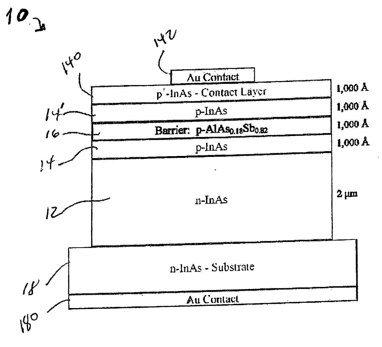
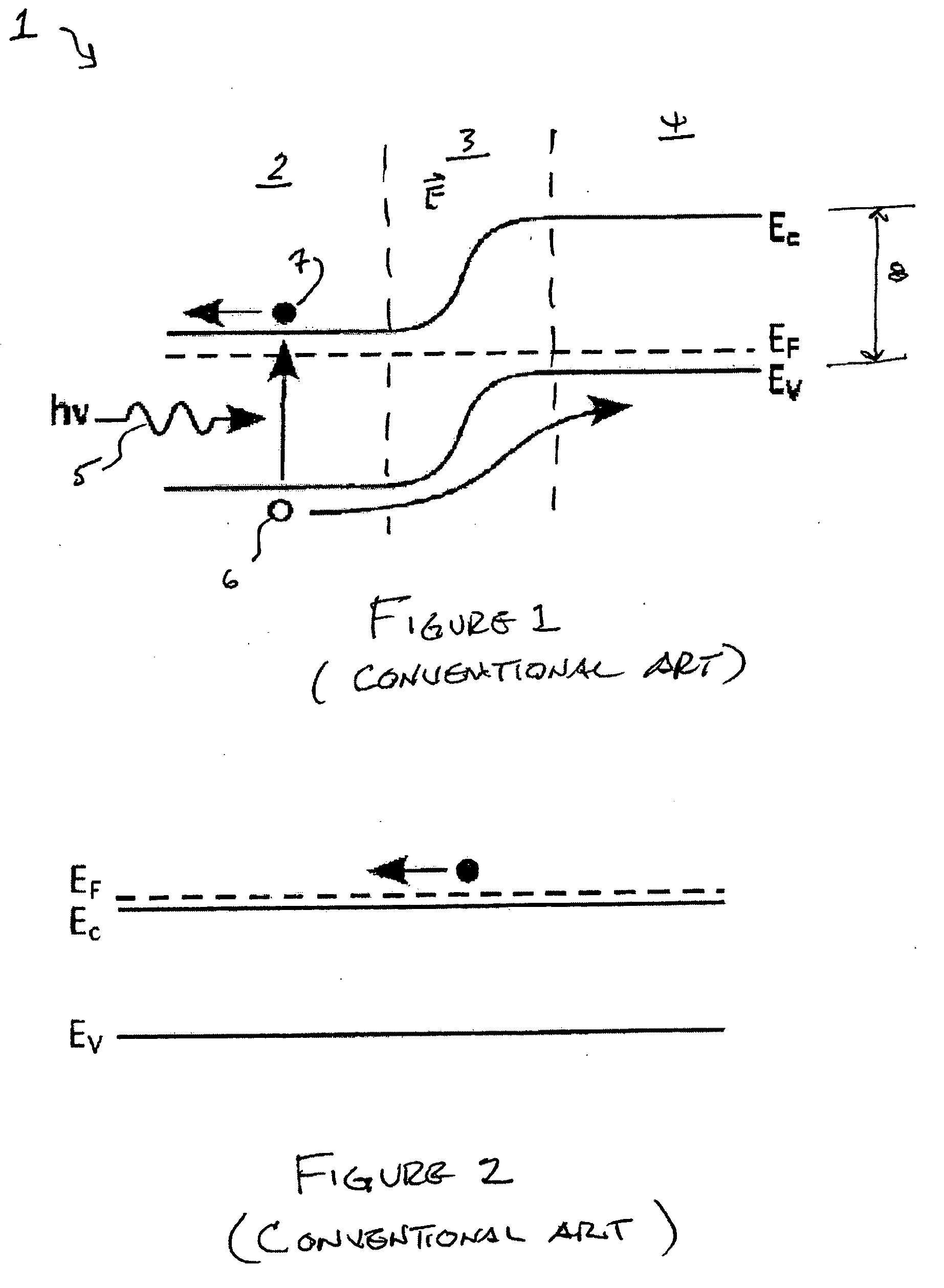
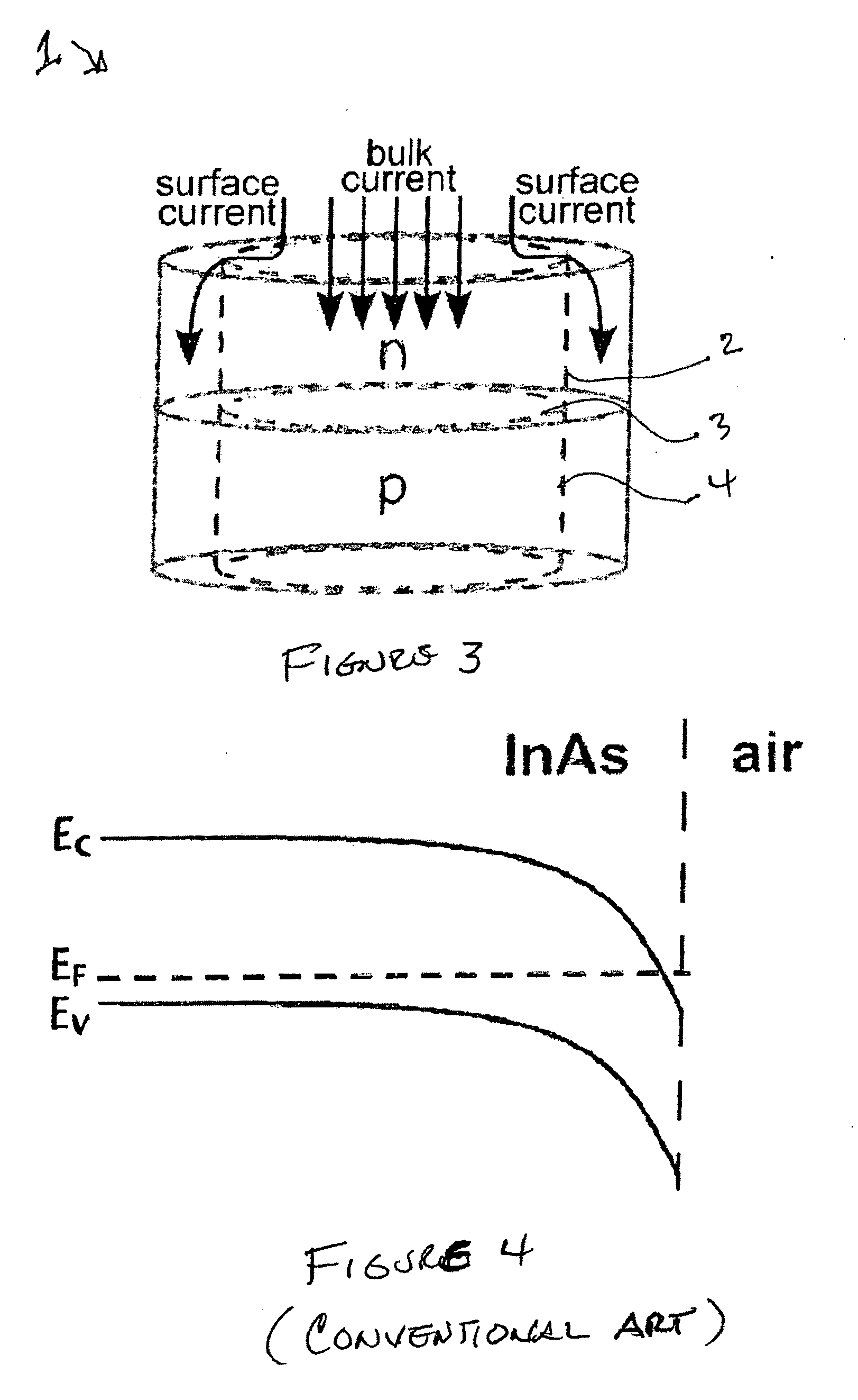
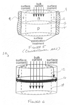
- The integration of unipolar barriers within the epitaxial structure of semiconductor devices during manufacturing, which blocks surface leakage currents while allowing bulk photocurrents to pass, eliminating the need for ex situ surface passivation treatments.
P-type materials and mixtures for electronic devices
PatentInactiveEP1463130A2
Innovation
- A p-type mixture comprising a dihydrophenazine compound as the host and a dopant, specifically designed to form a charge-transfer complex for efficient hole transport, is used in conjunction with an interfacial layer to prevent interdiffusion and maintain optical transparency and conductivity in OLEDs.


Sustainability Considerations in Semiconductor Materials
The semiconductor industry's environmental footprint has become increasingly significant as global production volumes continue to rise. When selecting materials for P-N junctions, sustainability considerations must now factor prominently alongside traditional performance metrics. The extraction and processing of semiconductor materials like silicon, gallium arsenide, and germanium involve substantial energy consumption and often generate hazardous waste products that require specialized disposal procedures.
Material selection for P-N junctions should prioritize elements with lower environmental impact during extraction and processing. Silicon remains the most sustainable mainstream semiconductor material due to its abundance in the earth's crust (approximately 28% by mass), reducing extraction-related environmental damage compared to rare earth elements. However, the purification process for silicon is energy-intensive, requiring temperatures exceeding 1400°C during zone refining.
Emerging alternatives such as organic semiconductors and carbon-based materials offer promising sustainability profiles. These materials typically require lower processing temperatures and utilize less toxic precursors. For instance, organic photovoltaic cells can be manufactured using solution-based processes at near-ambient temperatures, dramatically reducing energy requirements compared to traditional semiconductor fabrication.
End-of-life considerations represent another critical sustainability factor. Conventional semiconductor materials often contain toxic elements that complicate recycling efforts. Designing P-N junctions with recyclability in mind—utilizing separable components and minimizing hazardous dopants—can significantly improve lifecycle sustainability. Recent research indicates that up to 95% of semiconductor materials could theoretically be recovered through advanced recycling techniques.
Water usage presents a particular sustainability challenge, with traditional semiconductor manufacturing consuming between 2,000 and 5,000 gallons of ultra-pure water per wafer. Material selections that enable less water-intensive processing methods can dramatically reduce this environmental burden. Similarly, materials requiring fewer chemical etchants and solvents during processing reduce both pollution risks and resource consumption.
Energy efficiency during operation represents the final sustainability consideration. Materials enabling P-N junctions with lower resistance and better thermal characteristics reduce energy losses during device operation. This operational efficiency can offset higher initial environmental costs of material production, particularly for long-lifetime applications like power infrastructure components where devices may operate continuously for decades.
Manufacturing Process Compatibility Assessment
The compatibility of selected materials with established manufacturing processes represents a critical factor in p-n junction development. Silicon-based junctions benefit from decades of refined manufacturing techniques, including well-established diffusion, ion implantation, and epitaxial growth processes. These mature processes offer high yield rates exceeding 99% in modern fabrication facilities, significantly reducing production costs and ensuring consistent device performance.
When evaluating alternative semiconductor materials for p-n junctions, process integration challenges must be thoroughly assessed. Compound semiconductors such as GaAs, GaN, and SiC often require specialized equipment and modified processing parameters. For instance, GaN processing typically demands higher temperature tolerance (up to 1100°C) compared to silicon processes (typically 900-1000°C), necessitating specialized furnace equipment and thermal management protocols.
Material contamination risks present another significant manufacturing consideration. III-V compound semiconductors are particularly sensitive to cross-contamination in shared processing equipment. Dedicated fabrication lines may be required to prevent performance degradation, increasing initial capital investment by approximately 30-40% compared to utilizing existing silicon infrastructure.
Thermal budget constraints must be carefully evaluated when selecting p-n junction materials. The thermal expansion coefficient mismatch between different semiconductor materials and substrates can lead to mechanical stress and potential device failure during high-temperature processing steps. For example, the thermal expansion coefficient of GaAs (5.73×10^-6/K) differs significantly from silicon (2.6×10^-6/K), requiring specialized bonding techniques and thermal cycling protocols.
Dopant activation and diffusion characteristics vary substantially across semiconductor materials, affecting process window flexibility. Wide bandgap semiconductors typically require higher activation temperatures and exhibit lower dopant diffusion rates, necessitating precise process control systems with temperature uniformity within ±2°C across the wafer surface.
Etching selectivity and surface passivation requirements also differ significantly between material systems. For instance, III-V semiconductors often require specialized wet chemical etchants or reactive ion etching recipes with carefully calibrated gas mixtures to achieve desired feature profiles while maintaining surface integrity. Post-etching passivation processes must be material-specific to minimize surface states that could compromise junction electrical characteristics.
Ultimately, manufacturing process compatibility assessment must balance technical performance requirements against production economics. Novel materials offering superior electrical properties may face significant barriers to commercial adoption if they cannot leverage existing manufacturing infrastructure or require prohibitively expensive process modifications.
Unlock deeper insights with PatSnap Eureka Quick Research — get a full tech report to explore trends and direct your research. Try now!
Generate Your Research Report Instantly with AI Agent
Supercharge your innovation with PatSnap Eureka AI Agent Platform!