P–N Junction vs Schottky Diode: Efficiency in Power Devices
SEP 4, 20259 MIN READ
Generate Your Research Report Instantly with AI Agent
Patsnap Eureka helps you evaluate technical feasibility & market potential.
Junction Diode Evolution and Efficiency Goals
The evolution of junction diodes represents a significant milestone in the development of semiconductor technology. Since the discovery of the P-N junction in the early 1940s, these devices have undergone substantial transformations to meet the increasing demands of power applications. The initial germanium-based diodes gave way to silicon-based alternatives in the 1950s, offering improved thermal stability and reliability. By the 1960s, the introduction of Schottky diodes marked another pivotal advancement, providing faster switching capabilities and lower forward voltage drops compared to conventional P-N junction diodes.
The technological progression continued with the development of PIN diodes in the 1970s, which incorporated an intrinsic semiconductor layer between P and N regions to enhance power handling capabilities. The 1980s and 1990s witnessed the emergence of advanced manufacturing techniques, enabling the production of diodes with increasingly precise specifications and improved performance characteristics. More recently, wide bandgap materials such as silicon carbide (SiC) and gallium nitride (GaN) have revolutionized diode technology, pushing the boundaries of efficiency and power density.
Throughout this evolution, efficiency has remained a paramount concern, particularly in power applications where energy losses translate directly to operational costs and thermal management challenges. The efficiency goals for modern junction diodes encompass several critical parameters: minimizing forward voltage drop to reduce conduction losses, decreasing reverse recovery time to limit switching losses, enhancing thermal performance to improve reliability, and increasing power density to enable more compact designs.
For P-N junction diodes, efficiency targets focus on reducing the minority carrier lifetime while maintaining acceptable forward characteristics. This balance is crucial for applications requiring both low conduction losses and fast switching. Conversely, Schottky diode development aims to optimize the metal-semiconductor interface to achieve the lowest possible barrier height while maintaining high reverse breakdown voltage capabilities.
Current industry benchmarks target forward voltage drops below 0.7V for silicon P-N junction diodes and under 0.4V for Schottky diodes at rated currents. Reverse recovery times have progressively decreased from microseconds to nanoseconds, with modern fast-recovery diodes achieving recovery times below 50ns. Power density goals have similarly evolved, with contemporary designs striving for values exceeding 500W/cm².
Looking forward, the efficiency roadmap for junction diodes envisions further improvements through novel materials, innovative junction architectures, and advanced packaging solutions. The ultimate goal remains the development of "ideal" diodes that combine near-zero forward voltage drop with instantaneous switching capabilities and infinite reverse blocking voltage—a theoretical target that continues to drive research and development efforts in this critical component technology.
Market Demand Analysis for High-Efficiency Power Devices
The global power electronics market is experiencing robust growth, driven by increasing demand for energy-efficient power conversion systems across multiple industries. Current market valuations place this sector at approximately 40 billion USD in 2023, with projections indicating a compound annual growth rate of 6-8% through 2030. This growth trajectory is particularly significant for high-efficiency power devices, where the choice between P-N junction and Schottky diode technologies represents a critical decision point for manufacturers.
Consumer electronics continues to be a primary driver of market demand, with the proliferation of smartphones, tablets, and wearable devices requiring increasingly efficient power management solutions. The automotive sector presents perhaps the most dramatic growth opportunity, as electric vehicle adoption accelerates globally. EV power systems demand semiconductor components capable of handling high voltages and currents while minimizing energy losses, making diode selection particularly consequential.
Industrial automation and renewable energy systems represent additional high-growth segments. The industrial Internet of Things (IIoT) is creating unprecedented demand for power devices that can operate reliably in harsh environments while maintaining high efficiency. Similarly, solar inverters and wind power systems require power semiconductors that minimize conversion losses to maximize overall system efficiency.
Regional analysis reveals that Asia-Pacific dominates the market, accounting for over 45% of global demand, with China, Japan, and South Korea leading in both production and consumption. North America and Europe follow, with particular strength in automotive and industrial applications requiring premium performance characteristics.
End-user preferences increasingly favor solutions that minimize energy losses, reduce thermal management requirements, and enable smaller form factors. This has intensified interest in Schottky diodes, which offer lower forward voltage drop and faster switching capabilities compared to conventional P-N junction diodes, despite their higher cost and reverse leakage current limitations.
Market research indicates that efficiency improvements of even 1-2% in power conversion systems can translate to significant operational cost savings over device lifetimes, creating strong economic incentives for adopting more efficient technologies. This efficiency premium is particularly valued in applications with continuous operation or battery-powered devices where energy conservation directly impacts runtime.
Supply chain considerations are also influencing market dynamics, with recent semiconductor shortages highlighting the strategic importance of diversified component sourcing. This has prompted some manufacturers to maintain flexibility in design approaches, potentially utilizing both P-N junction and Schottky technologies depending on availability and application requirements.
Current State and Challenges in Diode Technologies
The diode technology landscape has evolved significantly over the past decades, with P-N junction and Schottky diodes representing two fundamental architectures that dominate power electronics applications. Currently, silicon-based P-N junction diodes remain the most widely deployed technology due to their established manufacturing processes, reliability, and cost-effectiveness. However, they face inherent limitations in switching speed and forward voltage drop, typically exhibiting values of 0.7-1.0V, which directly impacts power efficiency in high-frequency applications.
Schottky diodes have gained substantial market share in recent years, particularly in applications requiring high switching frequencies and lower power losses. Their metal-semiconductor junction design enables forward voltage drops as low as 0.15-0.45V and significantly faster switching capabilities due to the absence of minority carrier recombination processes. This technological advantage has positioned Schottky diodes as the preferred solution for power supplies, voltage regulators, and RF applications.
A significant challenge facing both technologies is thermal management. P-N junction diodes demonstrate superior thermal stability but suffer from temperature-dependent performance degradation. Schottky diodes, while more efficient at room temperature, experience dramatically increased leakage current at elevated temperatures, limiting their application in high-temperature environments without sophisticated cooling solutions.
Material limitations represent another critical challenge. Silicon-based diodes are approaching their theoretical performance limits, particularly regarding breakdown voltage and switching speed. This has accelerated research into wide bandgap (WBG) semiconductors such as silicon carbide (SiC) and gallium nitride (GaN), which promise to overcome these limitations. SiC Schottky diodes have already demonstrated remarkable performance improvements, with breakdown voltages exceeding 1700V and significantly reduced switching losses compared to silicon alternatives.
Geographically, diode technology development shows distinct patterns. Japan and Germany lead in high-precision silicon diode manufacturing, while the United States and China have made substantial investments in WBG semiconductor research and production facilities. Taiwan maintains dominance in high-volume manufacturing of conventional diodes, leveraging its established semiconductor ecosystem.
Miniaturization presents another significant challenge, particularly for power applications where heat dissipation becomes increasingly problematic as device dimensions shrink. Engineers must balance the competing demands of power handling capability, thermal management, and form factor requirements, often necessitating complex trade-offs in device design and application.
The integration of diodes into more complex power modules and systems introduces additional challenges related to parasitic effects, electromagnetic interference, and reliability under varying operational conditions. These system-level considerations often dictate the practical utility of theoretical performance advantages between P-N junction and Schottky technologies.
Comparative Analysis of P-N Junction and Schottky Solutions
01 Schottky diode structure optimization for improved efficiency
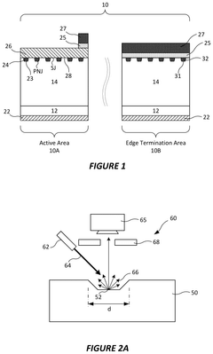
Optimizing the structure of Schottky diodes can significantly improve their efficiency. This includes modifications to the metal-semiconductor interface, barrier height engineering, and edge termination techniques. By carefully designing the contact area and implementing proper edge termination, leakage current can be reduced and breakdown voltage can be increased, leading to better overall performance and efficiency of the Schottky diode.- Schottky diode structure optimization for improved efficiency: Optimizing the structure of Schottky diodes can significantly improve their efficiency. This includes modifications to the metal-semiconductor interface, barrier height engineering, and edge termination techniques. By carefully designing the contact area and implementing proper junction isolation, leakage current can be reduced and forward bias performance enhanced. These structural optimizations lead to lower power losses and higher operating efficiencies in power conversion applications.
- P-N junction design enhancements for power applications: Enhanced P-N junction designs focus on improving carrier transport and reducing recombination losses. By optimizing doping profiles, junction depth, and implementing advanced fabrication techniques, the efficiency of power devices can be significantly improved. These enhancements enable faster switching speeds, lower on-resistance, and better thermal performance, which are critical for high-efficiency power conversion applications. Advanced P-N junction designs also incorporate features to manage electric field distribution and improve breakdown voltage characteristics.
- Novel materials and fabrication techniques for high-efficiency diodes: The introduction of novel semiconductor materials and advanced fabrication techniques has led to significant improvements in diode efficiency. Wide bandgap semiconductors such as SiC and GaN offer superior performance characteristics compared to traditional silicon. Additionally, innovative deposition methods, precise doping control, and nanoscale fabrication techniques enable the creation of optimized junction profiles. These advancements result in diodes with lower forward voltage drop, reduced reverse leakage current, and improved high-temperature performance.
- Integration of P-N junctions and Schottky diodes in power devices: The strategic integration of P-N junctions and Schottky diodes in power semiconductor devices combines the advantages of both technologies. This hybrid approach leverages the low forward voltage drop of Schottky diodes with the high blocking voltage capability of P-N junctions. Various integration architectures, including monolithic integration and co-packaging solutions, have been developed to optimize overall device performance. These integrated solutions offer improved switching characteristics, reduced recovery losses, and enhanced thermal management for high-efficiency power conversion systems.
- Surface treatment and passivation techniques for efficiency enhancement: Surface treatment and passivation techniques play a crucial role in enhancing the efficiency of both P-N junction and Schottky diodes. These methods focus on reducing surface states, interface traps, and recombination centers that degrade device performance. Advanced passivation layers, surface cleaning protocols, and interface engineering approaches help minimize leakage currents and improve carrier lifetime. Additionally, edge termination structures and guard rings implemented through precise surface treatments help manage electric field crowding and enhance breakdown voltage characteristics.
02 P-N junction design enhancements for power applications
Enhancing P-N junction designs for power applications involves optimizing doping profiles, junction depth, and semiconductor material selection. These enhancements can reduce on-resistance, improve current handling capability, and increase thermal stability. Advanced P-N junction designs incorporate features that minimize power losses during switching operations and improve overall energy conversion efficiency in power electronic applications.Expand Specific Solutions03 Integration of P-N junctions and Schottky diodes in semiconductor devices
The integration of P-N junctions and Schottky diodes in the same semiconductor device can leverage the advantages of both technologies. This approach allows for optimized switching speed, reduced forward voltage drop, and improved thermal performance. Hybrid designs that combine these junction types can be particularly effective in applications requiring both high-speed operation and power efficiency, such as in power converters and RF circuits.Expand Specific Solutions04 Novel materials and fabrication techniques for high-efficiency diodes
The use of novel materials and advanced fabrication techniques can significantly enhance diode efficiency. Wide bandgap semiconductors like SiC and GaN, as well as innovative heterostructures, offer superior performance characteristics compared to traditional silicon. Additionally, techniques such as selective epitaxial growth, atomic layer deposition, and precision doping methods enable the creation of diodes with optimized electrical properties and reduced defect densities, resulting in higher efficiency devices.Expand Specific Solutions05 Surface treatment and passivation methods for efficiency improvement
Surface treatment and passivation methods play a crucial role in improving diode efficiency by reducing surface recombination and interface states. Techniques such as hydrogen passivation, dielectric layer deposition, and surface cleaning processes can effectively minimize leakage currents and enhance carrier lifetime. These methods are particularly important for Schottky diodes where the metal-semiconductor interface quality directly impacts the device performance and efficiency.Expand Specific Solutions
Key Manufacturers and Competitive Landscape
The P-N Junction vs Schottky Diode competition in power devices is evolving rapidly, with the market entering a mature growth phase driven by electric vehicle and renewable energy demands. The global power semiconductor market exceeds $40 billion, with Schottky diodes gaining momentum due to superior switching efficiency. Leading companies like Infineon Technologies, Wolfspeed, and STMicroelectronics are advancing SiC and GaN Schottky technologies, while Alpha & Omega Semiconductor and ON Semiconductor focus on traditional silicon P-N junctions with incremental improvements. University partnerships with UESTC and Fudan University are accelerating next-generation device development, particularly in wide-bandgap semiconductors that promise higher efficiency and temperature tolerance for future power applications.
Wolfspeed, Inc.
Technical Solution: Wolfspeed has pioneered advanced silicon carbide (SiC) Schottky diode technology specifically designed for high-efficiency power applications. Their Z-Rec® series implements a proprietary merged-PIN-Schottky (MPS) cell design that combines the low forward voltage of Schottky barriers with improved surge capability of P-N junctions. This hybrid approach enables zero reverse recovery characteristics while maintaining robustness under surge conditions. Wolfspeed's latest generation devices feature optimized edge termination structures and advanced epitaxial layer engineering to achieve blocking voltages from 650V to 1700V with minimal leakage current. Their manufacturing process incorporates 150mm and 200mm SiC wafer technology with defect density reduction techniques that have improved yields by over 60% compared to earlier generations. The diodes demonstrate switching speeds approximately 3-5 times faster than silicon alternatives, with temperature coefficients specifically engineered to enable parallel operation without thermal runaway concerns.
Strengths: Industry-leading SiC substrate quality with lowest defect densities, enabling higher yield and reliability. Comprehensive product portfolio spanning multiple voltage classes and current ratings. Weaknesses: Premium pricing compared to silicon alternatives, and supply constraints due to high demand for SiC power devices across multiple industries.
Stmicroelectronics Srl
Technical Solution: STMicroelectronics has developed advanced power diode technologies addressing the P-N junction versus Schottky efficiency challenge through their STPOWER portfolio. Their silicon carbide (SiC) Schottky diode implementation features a proprietary design that combines a Schottky barrier with integrated junction barrier protection structures to optimize the trade-off between forward voltage drop and leakage current. ST's approach includes specialized edge termination techniques and guard ring structures that enable blocking voltages from 600V to 1700V while maintaining low forward voltage characteristics. Their manufacturing process incorporates defect screening methodologies that have improved reliability by reducing basal plane dislocations in the SiC substrate. ST's comparative testing demonstrates that replacing silicon P-N junction diodes with their SiC Schottky diodes in power conversion applications reduces switching losses by approximately 75% and enables operating frequencies up to 3x higher. Their latest generation devices feature optimized temperature coefficients that facilitate parallel operation and improved surge current capability up to 10x the nominal current rating.
Strengths: Vertical integration from SiC substrate to packaged devices ensures supply chain stability and quality control. Comprehensive portfolio spanning multiple voltage classes and current ratings enables one-stop shopping. Weaknesses: Higher cost structure compared to silicon alternatives, and thermal management challenges requiring careful system design to maximize benefits.
Core Patents and Innovations in Diode Efficiency
Semiconductor devices with integrated test areas
PatentPendingUS20240321647A1
Innovation
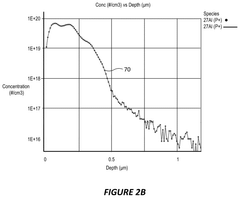
- Incorporating an integrated test area within the semiconductor device that allows for secondary ion mass spectrometry (SIMS) analysis to verify the implant doping profile, enabling direct material analysis on the production die and reducing the likelihood of device failure.
MOS p-n junction diode with enhanced response speed and manufacturing method thereof
PatentActiveUS20170133480A1
Innovation
- A method for manufacturing a MOS P-N junction diode with enhanced response speed involves forming a guard ring, central conductive layer, and metal diffusion layer, along with a polysilicon structure and silicon nitride layer, to reduce reverse recovery time while maintaining low reverse leakage current and high interface tolerance.
Thermal Management Considerations in Power Applications
Thermal management represents a critical factor in the performance and reliability of power devices, with significant differences between P-N junction diodes and Schottky diodes. The inherent physical structures of these devices directly impact their thermal characteristics and efficiency in power applications.
P-N junction diodes typically exhibit higher forward voltage drops (0.7-1.0V) compared to Schottky diodes (0.2-0.5V), resulting in greater power dissipation and heat generation during operation. This fundamental difference means P-N junction diodes generally require more robust thermal management solutions when implemented in high-current applications.
Schottky diodes demonstrate superior thermal efficiency due to their metal-semiconductor junction structure, which eliminates minority carrier storage effects present in P-N junctions. This absence of reverse recovery time translates to reduced switching losses and consequently lower heat generation during high-frequency operation, making them particularly advantageous in switch-mode power supplies and high-frequency rectification applications.
Temperature coefficient characteristics also differ significantly between these device types. P-N junction diodes exhibit a negative temperature coefficient for forward voltage, which can lead to thermal runaway concerns in parallel configurations. Conversely, Schottky diodes typically display a positive temperature coefficient, providing better current sharing capabilities in parallel arrangements and enhanced thermal stability.
Junction temperature limitations present another important consideration. While silicon P-N junction diodes can typically operate at junction temperatures up to 175°C, Schottky diodes generally have lower maximum junction temperature ratings (typically 125-150°C). This limitation necessitates more careful thermal design when implementing Schottky solutions in high-temperature environments.
Package selection and thermal interface materials become particularly important for Schottky diodes in high-power applications. Advanced packaging technologies like DirectFET and bottom-cooled designs have emerged specifically to address the thermal challenges of these devices, allowing them to operate more efficiently in compact power conversion systems.
The emergence of wide bandgap semiconductor materials like silicon carbide (SiC) has further revolutionized thermal management considerations. SiC Schottky diodes combine the switching benefits of traditional Schottky structures with significantly improved thermal conductivity and higher temperature operation capabilities, enabling more compact thermal solutions in advanced power applications.
Material Science Advancements for Next-Gen Diodes
Recent advancements in material science have revolutionized diode technology, particularly in the ongoing competition between P-N junction and Schottky diodes for power applications. Traditional silicon-based semiconductors are increasingly being supplemented or replaced by wide bandgap (WBG) materials such as silicon carbide (SiC) and gallium nitride (GaN), which demonstrate superior performance characteristics in high-power and high-frequency applications.
For P-N junction diodes, the introduction of silicon carbide has enabled significant improvements in thermal conductivity and breakdown voltage. SiC-based P-N diodes can operate at temperatures exceeding 200°C while maintaining excellent electrical characteristics, a substantial improvement over conventional silicon alternatives limited to approximately 150°C. These advancements have been achieved through refined epitaxial growth techniques and improved doping control methodologies.
Schottky diodes have benefited even more dramatically from material science innovations. The metal-semiconductor interface, critical to Schottky diode performance, has seen remarkable improvements through novel metallization schemes. Titanium, nickel, and platinum silicides have demonstrated enhanced barrier heights and reduced leakage currents. Additionally, edge termination techniques using field plates and guard rings have substantially improved voltage handling capabilities.
Nanostructured materials represent another frontier in diode development. Carbon nanotubes and graphene are being investigated as potential materials for ultra-fast Schottky diodes due to their exceptional electron mobility characteristics. Early prototypes have demonstrated switching speeds in the terahertz range, potentially enabling next-generation high-frequency applications.
Heterojunction engineering has emerged as a promising approach for both diode types. By carefully controlling the interface between different semiconductor materials, researchers have created devices with customized electrical properties. AlGaN/GaN heterojunctions, for example, have demonstrated exceptional electron mobility and power handling capabilities in Schottky configurations.
Surface passivation technologies have also advanced significantly, addressing historical reliability challenges in both diode types. Atomic layer deposition (ALD) techniques now allow for nanometer-precision application of passivation layers, dramatically reducing surface states and leakage currents. For Schottky diodes specifically, these improvements have narrowed the efficiency gap with P-N junction alternatives.
Looking forward, emerging materials such as diamond semiconductors and gallium oxide (Ga₂O₃) show tremendous potential for next-generation diodes. Diamond's unparalleled thermal conductivity (approximately 2000 W/mK) and breakdown field strength (10 MV/cm) could theoretically enable power devices with performance metrics far exceeding current technologies, though commercialization challenges remain significant.
Unlock deeper insights with Patsnap Eureka Quick Research — get a full tech report to explore trends and direct your research. Try now!
Generate Your Research Report Instantly with AI Agent
Supercharge your innovation with Patsnap Eureka AI Agent Platform!