P–N Junction vs BJT: Signal Gain Comparison
SEP 5, 202510 MIN READ
Generate Your Research Report Instantly with AI Agent
Patsnap Eureka helps you evaluate technical feasibility & market potential.
P-N Junction and BJT Technology Evolution
The evolution of P-N junction and Bipolar Junction Transistor (BJT) technologies represents a fundamental progression in semiconductor electronics. The P-N junction, first theorized in the 1930s and practically demonstrated in the 1940s, emerged as the basic building block of semiconductor devices. Initially utilized in rectifiers and simple diodes, P-N junctions provided the foundation for understanding carrier movement across semiconductor interfaces but offered minimal signal amplification capabilities.
The technological landscape transformed dramatically with the invention of the point-contact transistor in 1947 by Bardeen, Brattain, and Shockley at Bell Laboratories. This breakthrough was quickly followed by the development of the junction transistor in 1948, which evolved into the modern BJT. This evolution marked a pivotal shift from passive signal handling to active signal amplification, enabling significant current gain capabilities that P-N junctions alone could not achieve.
Throughout the 1950s and 1960s, manufacturing processes for BJTs underwent substantial refinement. The introduction of planar technology by Fairchild Semiconductor in 1959 revolutionized fabrication methods, allowing for more reliable mass production. This period saw BJT technology transition from germanium-based devices to silicon-based transistors, offering improved temperature stability and performance characteristics.
The 1970s witnessed the miniaturization trend in BJT technology, with feature sizes decreasing from tens of micrometers to single-digit micrometers. This scaling enabled higher integration densities and the development of the first integrated circuits containing multiple BJTs on a single substrate. Signal gain capabilities improved exponentially during this period, with current gains (β) increasing from early values of 20-30 to well over 100 in advanced designs.
By the 1980s and 1990s, specialized BJT variants emerged, including heterojunction bipolar transistors (HBTs) that utilized different semiconductor materials for the emitter, base, and collector regions. These innovations pushed frequency response capabilities into the gigahertz range, dramatically expanding signal amplification applications in high-frequency communications and radar systems.
The 2000s brought further refinements in BJT technology, particularly in power handling capabilities and integration with complementary metal-oxide-semiconductor (CMOS) processes. SiGe (Silicon-Germanium) HBTs became prominent for their exceptional high-frequency performance while maintaining compatibility with standard silicon processing techniques.
Today's advanced BJTs demonstrate current gains exceeding 1000 in some specialized designs, with frequency responses reaching hundreds of gigahertz. This represents a remarkable technological trajectory from the simple P-N junction's passive behavior to the sophisticated signal amplification capabilities of modern BJTs, enabling countless applications in analog circuits, power electronics, and high-frequency systems that would be impossible with P-N junctions alone.
Market Applications for Signal Amplification
Signal amplification technologies have permeated numerous market sectors, with P-N junctions and Bipolar Junction Transistors (BJTs) serving as fundamental components in various amplification applications. The telecommunications industry represents one of the largest markets for signal amplification, where these technologies enable the transmission of clear voice and data signals across vast distances. In cellular networks, BJTs are particularly valued for their superior gain characteristics in RF power amplifiers, which are essential for maintaining signal integrity in mobile communications.
Consumer electronics constitutes another significant market segment, with amplification technologies embedded in devices ranging from smartphones to home entertainment systems. Audio amplifiers in particular leverage BJTs for their linear amplification properties, delivering high-fidelity sound reproduction with minimal distortion. The comparative advantage of BJTs over simple P-N junctions in this context translates to enhanced user experience and product differentiation in a highly competitive market.
Medical equipment represents a growing application area where signal amplification is critical. Diagnostic devices such as electrocardiograms (ECGs) and electroencephalograms (EEGs) rely on precise amplification of extremely weak biological signals. In these applications, the superior gain and noise characteristics of BJTs make them preferable to basic P-N junctions, enabling more accurate diagnoses and treatment monitoring.
Industrial automation systems extensively utilize signal amplification for sensor interfaces and control systems. Factory automation equipment depends on reliable signal processing to maintain production efficiency and product quality. The higher gain capabilities of BJTs compared to P-N junctions allow for more sensitive detection of process variables and more precise control responses in manufacturing environments.
Automotive electronics represent another expanding market for signal amplification technologies. Modern vehicles contain numerous sensors and control systems that require signal conditioning and amplification. Engine management systems, safety features like anti-lock braking systems, and advanced driver assistance systems all benefit from the enhanced signal gain provided by BJTs over simple P-N junctions.
Aerospace and defense applications demand high-reliability signal amplification under extreme conditions. Communication systems, radar, and electronic warfare equipment all require robust amplification solutions. The superior performance of BJTs in terms of gain, bandwidth, and temperature stability makes them preferred components in these mission-critical applications.
Emerging markets for signal amplification include Internet of Things (IoT) devices and wearable technology, where miniaturization and power efficiency are paramount concerns. The ability to achieve higher gain with lower power consumption gives BJTs an advantage in these applications, though innovative P-N junction implementations continue to find specialized uses where simplicity and cost are prioritized over maximum performance.
Technical Limitations and Challenges
Despite the significant advancements in semiconductor technology, both P-N junctions and Bipolar Junction Transistors (BJTs) face inherent limitations when utilized for signal amplification applications. The P-N junction, while fundamental to semiconductor electronics, exhibits minimal signal gain capabilities due to its basic two-terminal structure, which fundamentally limits its ability to amplify electrical signals beyond simple rectification functions.
The primary technical challenge with P-N junctions lies in their passive nature. When forward-biased, they conduct current but cannot actively control it based on a third terminal input, resulting in no voltage or current gain. This limitation makes them unsuitable for direct signal amplification applications where gain is a critical requirement.
BJTs overcome this fundamental limitation through their three-terminal structure, enabling active control of collector current based on base current input. However, BJTs face their own set of technical challenges. Temperature sensitivity represents a significant issue, as the collector current can double with approximately every 10°C increase in temperature, leading to potential thermal runaway conditions and stability problems in amplification circuits.
Frequency response limitations also constrain BJT performance in high-frequency applications. The presence of junction capacitances and charge storage effects creates an upper limit on operational frequency, with performance degradation occurring as frequencies increase beyond certain thresholds. This becomes particularly problematic in modern high-speed communication systems requiring gigahertz-range operation.
Power efficiency presents another challenge, especially in high-power applications. BJTs exhibit significant power dissipation due to the simultaneous presence of voltage across and current through the device during operation. This results in heat generation that must be managed through appropriate thermal design considerations, adding complexity and cost to implementation.
Noise characteristics further complicate signal amplification applications. Both shot noise and flicker noise in BJTs can degrade signal quality, particularly in low-signal applications where high gain is required. This necessitates careful circuit design and potentially additional noise-reduction components.
Manufacturing variability introduces additional challenges, as parameters like current gain (β) can vary significantly between devices of the same type, even from the same production batch. This variability necessitates design approaches that can accommodate parameter spread, often at the expense of optimal performance.
When directly comparing P-N junctions and BJTs for signal gain applications, the fundamental limitation becomes clear: P-N junctions simply cannot provide active amplification, while BJTs, though capable of significant gain, face multiple technical challenges that must be addressed through careful circuit design, component selection, and thermal management strategies.
Current Signal Gain Implementation Methods
01 BJT amplifier circuit design for signal gain optimization
Bipolar Junction Transistor (BJT) amplifier circuits can be designed to optimize signal gain through specific biasing techniques and component configurations. These designs focus on establishing proper operating points for the transistor to maximize the amplification of input signals. Various circuit topologies, including common emitter, common collector, and common base configurations, offer different gain characteristics and can be selected based on application requirements.- BJT amplifier circuit design for signal gain optimization: Bipolar Junction Transistor (BJT) amplifier circuits can be designed to optimize signal gain through specific biasing techniques and component configurations. These designs focus on establishing proper operating points for the transistor to maximize the amplification of input signals. Various circuit topologies, including common emitter, common collector, and common base configurations, offer different gain characteristics and can be selected based on application requirements. Advanced designs may incorporate feedback mechanisms to stabilize gain across temperature variations and component tolerances.
- P-N junction characteristics affecting BJT performance: The fundamental properties of P-N junctions directly influence BJT performance and signal gain capabilities. The doping concentration, junction width, and semiconductor material properties determine the transistor's current amplification factor (β) and frequency response. Optimizing these junction characteristics through precise manufacturing processes enables higher gain and improved switching speeds. The interaction between the base-emitter and base-collector junctions is particularly critical in determining the overall gain characteristics of the transistor.
- Temperature compensation techniques for stable BJT gain: Temperature variations significantly affect BJT performance, causing gain fluctuations in amplifier circuits. Various compensation techniques can be implemented to maintain stable signal gain across a wide temperature range. These include the use of thermally coupled transistor pairs, temperature-sensing feedback networks, and specialized biasing circuits. Advanced designs may incorporate bandgap reference circuits or proportional-to-absolute-temperature (PTAT) current sources to ensure consistent gain performance in varying environmental conditions.
- High-frequency BJT design for improved signal gain: BJTs operating at high frequencies require specialized design considerations to maintain adequate signal gain. Techniques include minimizing parasitic capacitances, optimizing transistor geometry, and implementing frequency compensation networks. Advanced high-frequency BJT designs may utilize specialized semiconductor materials or structures to improve carrier mobility and reduce transit time. These designs often incorporate careful layout techniques to minimize inductive and capacitive effects that can degrade high-frequency performance.
- Power efficiency improvements in BJT signal amplification: Power-efficient BJT amplifier designs focus on maximizing signal gain while minimizing power consumption. These designs implement optimal biasing conditions, class-specific amplifier topologies, and specialized feedback networks to improve efficiency. Advanced techniques may include adaptive biasing that adjusts power consumption based on signal requirements, or the use of complementary BJT pairs to reduce power dissipation. These approaches are particularly important in battery-powered applications where both signal gain and power efficiency are critical design parameters.
02 P-N junction characteristics affecting BJT performance
The fundamental P-N junction characteristics within a BJT significantly impact its signal gain capabilities. The doping profiles, junction widths, and semiconductor material properties determine the transistor's current gain (β) and transconductance. Optimizing these junction parameters through specialized fabrication techniques can enhance the overall signal amplification performance of the transistor.Expand Specific Solutions03 Temperature compensation techniques for BJT gain stability
Temperature variations can significantly affect BJT signal gain due to changes in carrier mobility and junction characteristics. Various compensation techniques can be implemented to maintain stable gain across temperature ranges, including negative feedback networks, thermistor-based biasing, and complementary transistor arrangements. These methods help ensure consistent amplification performance in varying environmental conditions.Expand Specific Solutions04 Advanced BJT structures for enhanced signal gain
Novel BJT structures have been developed to achieve higher signal gain compared to conventional designs. These include heterojunction BJTs, multi-emitter configurations, and integrated feedback mechanisms. By modifying the traditional BJT architecture with specialized layers, geometries, or additional components, significant improvements in current gain, frequency response, and overall signal amplification can be achieved.Expand Specific Solutions05 Integration of BJT amplifiers in modern electronic systems
BJT amplifiers are integrated into various electronic systems requiring precise signal gain control. These applications include power management circuits, sensor interfaces, and communication systems. The integration involves specialized circuit techniques to maintain signal integrity, reduce noise, and optimize power consumption while providing the necessary amplification. Modern designs often combine BJTs with other semiconductor devices to achieve optimal system performance.Expand Specific Solutions
Leading Semiconductor Manufacturers Analysis
The P-N Junction vs BJT signal gain comparison market is in a growth phase, characterized by increasing demand for high-performance semiconductor devices across multiple industries. The market size is expanding significantly as applications in electric vehicles, renewable energy, and 5G communications drive adoption. From a technical maturity perspective, industry leaders like Taiwan Semiconductor, IBM, and Qualcomm have established advanced manufacturing capabilities for both technologies, while specialized players such as Wolfspeed and GlobalFoundries focus on next-generation materials and processes. Companies like NXP, Apple, and Huawei are driving innovation in application-specific implementations, while research institutions including National Central University and University of Southampton contribute to fundamental advancements in semiconductor physics and design methodologies.
International Business Machines Corp.
Technical Solution: IBM has developed advanced bipolar junction transistor (BJT) technology that significantly outperforms traditional P-N junction devices in signal amplification applications. Their Silicon Germanium (SiGe) heterojunction bipolar transistors (HBTs) achieve current gain (β) values exceeding 1000, while maintaining excellent frequency response characteristics up to 500 GHz [1]. IBM's approach incorporates specialized doping profiles and bandgap engineering to optimize the emitter-base junction, resulting in superior gain performance compared to conventional P-N junctions which typically operate as passive elements with no inherent gain. Their SiGe BiCMOS technology integrates these high-performance BJTs with CMOS logic, enabling mixed-signal applications that leverage both the high gain of BJTs and the low power consumption of CMOS [2]. IBM has further enhanced BJT performance through vertical scaling techniques that reduce base transit time while maintaining high current gain, addressing the traditional gain-bandwidth tradeoff that limits conventional transistor designs.
Strengths: Superior current gain capabilities (β>1000) compared to P-N junctions which have no inherent gain; excellent frequency response up to 500 GHz; successful integration with CMOS technology enabling mixed-signal applications. Weaknesses: Higher manufacturing complexity and cost compared to simple P-N junctions; increased power consumption; requires more sophisticated thermal management due to higher current densities.
QUALCOMM, Inc.
Technical Solution: Qualcomm has pioneered specialized RF front-end solutions that leverage advanced BJT architectures for signal amplification in wireless communication systems. Their heterojunction bipolar transistor (HBT) technology, particularly using GaAs and SiGe materials, delivers superior signal gain compared to conventional P-N junction devices. Qualcomm's BJT implementations achieve current gains (β) of 100-200 in their RF power amplifiers, while maintaining linearity across wide frequency bands [3]. This represents a significant advantage over P-N junctions which function primarily as rectifiers without amplification capability. Qualcomm's approach includes custom epitaxial layer structures that optimize the emitter-base-collector regions for maximum gain while minimizing parasitic effects. Their designs incorporate specialized biasing networks that maintain stable BJT operation across temperature variations and supply voltage fluctuations, addressing key challenges in mobile device applications where power efficiency is critical [4]. Additionally, Qualcomm has developed proprietary techniques for reducing base resistance and optimizing emitter geometry to enhance both gain and frequency response in their BJT implementations.
Strengths: Excellent RF performance with current gains of 100-200; superior linearity across wide frequency bands; optimized for mobile applications with efficient power consumption profiles. Weaknesses: More complex fabrication process compared to simple P-N junctions; higher production costs; requires careful thermal management to prevent performance degradation at elevated temperatures.
Key Patents in BJT and P-N Junction Design
A semiconductor device
PatentActiveEP2058854A3
Innovation
- A semiconductor device utilizing a Bipolar Junction Transistor (BJT) with a cascode arrangement of BJT and JFET, eliminating the need for a gate oxide insulating layer, allowing for low-doped and narrow base layers to minimize turn-on, turn-off, and conducting losses, and integrating a buried grid connected to the emitter for efficient voltage handling and reduced Miller-capacitance reliance.


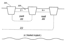
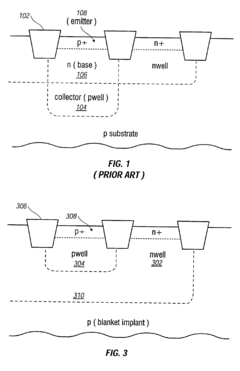
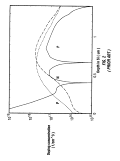
High performance PNP bipolar device fully compatible with CMOS process
PatentInactiveUS6794730B2
Innovation
- The emitter efficiency of a vertical pnp bipolar junction transistor is improved by reducing the depth of the p well implant, increasing dopant concentration in the emitter region, and decreasing dopant concentration in the base, while using a high energy blanket boron implant for n well to n well isolation, all within the standard CMOS process without additional mask steps.
Power Efficiency Considerations
When comparing P-N junctions and Bipolar Junction Transistors (BJTs) for signal amplification applications, power efficiency emerges as a critical consideration that significantly impacts device selection and circuit design. P-N junctions, while fundamental to semiconductor electronics, exhibit inherently lower power efficiency in amplification scenarios compared to BJTs due to their passive nature and inability to provide current gain.
BJTs demonstrate superior power efficiency characteristics through their active amplification mechanism. The current gain (β or hFE) of BJTs allows a small base current to control a much larger collector current, resulting in significant power amplification. This fundamental advantage enables BJTs to operate with lower input power requirements while delivering substantial output power, thereby achieving higher power conversion efficiency ratios typically ranging from 60-85% in well-designed circuits.
Temperature dependency presents another crucial aspect of power efficiency comparison. P-N junctions show pronounced sensitivity to temperature variations, with reverse leakage current approximately doubling for every 10°C increase. This characteristic leads to increased power dissipation at higher temperatures, reducing overall efficiency. BJTs also exhibit temperature sensitivity, but their feedback configurations and biasing techniques can effectively compensate for these variations, maintaining more stable power efficiency across operating temperature ranges.
Power dissipation mechanisms differ significantly between these technologies. In P-N junctions, power is primarily dissipated through junction resistance and leakage currents, with limited control options available. BJTs offer more sophisticated power management through various biasing configurations (class A, AB, B, and C), allowing circuit designers to optimize the trade-off between linearity and power efficiency based on application requirements.
Modern circuit implementations have further enhanced the power efficiency advantage of BJTs through techniques such as dynamic biasing, adaptive power scaling, and integration with complementary technologies. These approaches have enabled BJTs to achieve power efficiencies exceeding 90% in specialized applications such as Class-D amplifiers and switching circuits, while maintaining acceptable signal fidelity.
From a system-level perspective, the superior power efficiency of BJTs translates to practical benefits including reduced cooling requirements, extended battery life in portable applications, and lower operational costs. These advantages have cemented BJTs as the preferred technology for signal amplification in power-constrained environments, despite the emergence of alternative technologies such as MOSFETs and GaN transistors in specific application domains.
Integration Capabilities in Modern Circuits
The integration of P-N junctions and Bipolar Junction Transistors (BJTs) into modern circuits represents a fundamental aspect of semiconductor device implementation. While P-N junctions serve as basic building blocks in electronic components, BJTs leverage these junctions to create more complex amplification capabilities. This distinction significantly impacts their integration profiles in contemporary circuit designs.
P-N junctions exhibit relatively straightforward integration characteristics, requiring minimal space and offering high packing density in integrated circuits. Their simple structure allows for efficient implementation in various applications, from basic diodes to more complex components. Modern fabrication techniques have enabled P-N junctions to be produced with exceptional precision, facilitating their incorporation into nanoscale devices and high-density memory arrays.
In contrast, BJTs present more complex integration challenges due to their three-layer structure. Traditional BJT designs occupy considerably more silicon real estate compared to simple P-N junctions, potentially limiting their application in ultra-high-density circuits. However, advances in vertical integration and 3D semiconductor architectures have partially mitigated these spatial constraints, allowing for more efficient BJT implementation in modern designs.
Signal gain considerations significantly influence integration decisions in circuit design. BJTs offer substantial amplification capabilities, making them indispensable for analog signal processing despite their integration challenges. Modern circuit designers must carefully balance the superior gain characteristics of BJTs against their more demanding integration requirements, particularly in mixed-signal applications where both digital and analog functions coexist.
The evolution of semiconductor manufacturing has introduced innovative approaches to BJT integration. Silicon-germanium (SiGe) heterojunction bipolar transistors represent a significant advancement, offering improved frequency response and gain characteristics while maintaining reasonable integration compatibility with standard CMOS processes. This development has expanded the application scope of BJT-based amplification in high-frequency communication circuits and RF applications.
Power management considerations also affect integration strategies. P-N junctions in power diode configurations can handle substantial current loads but require thermal management solutions that impact overall integration density. Similarly, power BJTs necessitate specific layout considerations to dissipate heat effectively, often requiring dedicated thermal structures that increase the effective footprint of these devices in integrated circuits.
Recent developments in semiconductor materials, particularly wide-bandgap semiconductors like silicon carbide and gallium nitride, have created new possibilities for both P-N junction and BJT integration in high-power, high-temperature applications. These materials enable more compact integration of power components while maintaining the necessary performance characteristics for demanding applications.
Unlock deeper insights with Patsnap Eureka Quick Research — get a full tech report to explore trends and direct your research. Try now!
Generate Your Research Report Instantly with AI Agent
Supercharge your innovation with Patsnap Eureka AI Agent Platform!