P–N Junction in Power Electronics: Thermal Load Handling
SEP 12, 202510 MIN READ
Generate Your Research Report Instantly with AI Agent
Patsnap Eureka helps you evaluate technical feasibility & market potential.
P-N Junction Thermal Management Background and Objectives
The P-N junction represents one of the most fundamental structures in semiconductor physics and serves as the cornerstone for numerous power electronic devices. Since its discovery in the early 20th century, this interface between p-type and n-type semiconductors has evolved from a theoretical concept to an essential component in modern power electronics. The historical trajectory of P-N junction development has been characterized by continuous improvements in material science, fabrication techniques, and thermal management strategies.
The thermal behavior of P-N junctions has become increasingly critical as power electronic applications demand higher power densities, faster switching speeds, and greater reliability. Early power devices operated at relatively low power densities, with thermal management being a secondary consideration. However, as applications expanded into automotive, renewable energy, and industrial sectors, the ability to handle thermal loads emerged as a primary design constraint.
Current technological trends indicate a push toward wide bandgap semiconductors such as silicon carbide (SiC) and gallium nitride (GaN), which offer superior thermal conductivity compared to traditional silicon. These materials allow P-N junctions to operate at higher temperatures, potentially reaching 300°C for SiC compared to silicon's typical 150°C limit. This evolution represents a significant paradigm shift in thermal management approaches.
The primary objective of thermal load handling in P-N junctions is to maintain junction temperature below critical thresholds while maximizing power throughput. This delicate balance requires comprehensive understanding of heat generation mechanisms, thermal resistance pathways, and cooling strategies. Specifically, research aims to characterize and mitigate three primary heat sources: ohmic heating from current flow, recombination heating at the junction, and switching losses during state transitions.
Another crucial objective is the development of accurate thermal models that can predict temperature distributions across the junction under various operating conditions. These models must account for the non-linear thermal behavior of semiconductor materials and the complex three-dimensional heat flow patterns that develop during operation. Advanced simulation techniques incorporating finite element analysis have become essential tools in this pursuit.
Looking forward, the field aims to establish standardized thermal characterization methodologies that enable meaningful comparison between different junction designs and materials. Additionally, there is growing interest in dynamic thermal management strategies that can adapt to changing operational demands, potentially extending device lifetimes and improving overall system reliability.
Market Demand Analysis for Thermally Efficient Power Electronics
The power electronics market is experiencing unprecedented growth driven by the electrification trend across multiple industries. Current market analysis indicates that the global power electronics market is projected to reach $49.3 billion by 2027, growing at a CAGR of 5.7% from 2022. Within this broader market, thermally efficient power electronics components represent a rapidly expanding segment due to their critical role in system reliability and performance.
The automotive sector stands as a primary demand driver, with electric vehicles requiring increasingly efficient power management systems. The EV market's compound annual growth rate of approximately 24% directly translates to heightened demand for thermally optimized P-N junction devices capable of handling the high-power density requirements of modern electric drivetrains. Industry reports indicate that thermal management solutions specifically for power electronics in EVs constitute a $3.2 billion market segment with projected growth exceeding 30% annually.
Renewable energy systems represent another significant market vertical, with solar inverters and wind power converters requiring robust thermal load handling capabilities. The global solar inverter market alone is valued at $12.8 billion with thermal management components accounting for approximately 18% of system costs. As renewable installations continue to scale, demand for thermally efficient power electronics is expected to grow at 15% annually through 2030.
Industrial automation and data center infrastructure collectively contribute to market expansion, with an estimated 22% of operational failures in these sectors attributed to thermal issues in power electronic components. This has created a specialized market for thermally enhanced P-N junction technologies valued at $5.7 billion with particularly strong demand in regions experiencing high ambient temperatures.
Consumer electronics manufacturers are increasingly prioritizing thermal efficiency in power management circuits, driven by the trend toward faster charging technologies and higher power density requirements. The fast-charging market segment is growing at 26% annually, with thermal management solutions representing a critical differentiator for competitive products.
Regional analysis reveals that Asia-Pacific dominates manufacturing capacity for thermally efficient power electronics, accounting for 63% of global production. However, North America and Europe lead in research and development investments, with combined annual R&D expenditure of $4.2 billion specifically targeting thermal load handling improvements in semiconductor devices.
Market forecasts indicate that demand for silicon carbide and gallium nitride-based power electronics with enhanced thermal properties will grow at 35% annually, outpacing traditional silicon-based solutions. This shift is primarily driven by applications requiring operation in extreme temperature environments and those demanding higher power density with minimal cooling infrastructure.
Current Thermal Load Challenges in P-N Junction Technology
Power electronic devices based on P-N junctions face significant thermal load challenges that limit their performance and reliability. The primary issue stems from the inherent physics of semiconductor operation, where current flow across the junction generates heat through various mechanisms. Joule heating, resulting from resistive losses as carriers traverse the semiconductor material, represents the most substantial thermal contribution. This effect intensifies with increasing current density, creating localized hotspots that can compromise device integrity.
Switching losses present another critical thermal challenge, particularly in high-frequency applications. During state transitions, power devices experience momentary conditions where voltage and current are simultaneously high, resulting in significant energy dissipation. Modern power electronics systems operating at increasingly higher switching frequencies to reduce passive component sizes face compounded thermal management difficulties due to this phenomenon.
Thermal runaway represents perhaps the most dangerous thermal challenge in P-N junction devices. As temperature increases, intrinsic carrier concentration rises exponentially, potentially triggering a self-reinforcing cycle of increased leakage current, additional heat generation, and further temperature elevation. Without adequate thermal management, this process can rapidly escalate to catastrophic device failure.
Non-uniform temperature distribution across device structures creates thermal gradients that induce mechanical stress through differential thermal expansion. These stresses can lead to package delamination, wire bond failures, die cracking, and solder fatigue. The cyclical nature of many power applications exacerbates this issue through thermal cycling, which accelerates wear mechanisms and reduces device lifetime.
Current density limitations represent a fundamental constraint in P-N junction technology. As devices are pushed to handle higher power densities, the junction temperature rises accordingly. Most silicon-based power devices are limited to operating temperatures below 175°C, with reliability concerns emerging well before this threshold. This thermal ceiling effectively caps the maximum current density achievable in conventional devices.
Package thermal resistance constitutes a significant bottleneck in heat dissipation pathways. Traditional packaging technologies struggle to efficiently extract heat from increasingly power-dense semiconductor dies. The thermal interface materials between die, substrate, and heatsink introduce additional thermal resistances that impede heat flow and contribute to temperature rise at the junction.
Advanced wide-bandgap semiconductors like SiC and GaN offer improved thermal performance but introduce new challenges related to packaging, reliability assessment, and cost-effective manufacturing. These materials can theoretically operate at higher temperatures but require innovative thermal management solutions to fully realize their potential in practical applications.
Current Thermal Load Handling Techniques for P-N Junctions
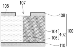
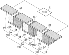
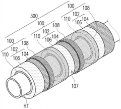
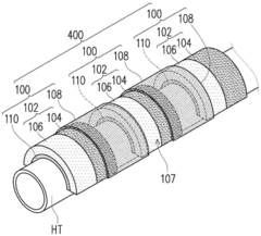
01 Heat dissipation structures for P-N junctions
Various heat dissipation structures can be implemented to manage thermal loads in P-N junctions. These include heat sinks, thermal vias, and specialized packaging designs that efficiently transfer heat away from the junction. Improved thermal management structures help maintain optimal operating temperatures, prevent thermal runaway, and extend the lifespan of semiconductor devices by reducing thermal stress at the junction interface.- Heat dissipation structures for P-N junctions: Various heat dissipation structures can be implemented to manage thermal loads in P-N junctions. These structures include heat sinks, thermal vias, and specialized packaging designs that efficiently transfer heat away from the junction. By incorporating these elements, the thermal resistance between the junction and the ambient environment is reduced, allowing for better temperature regulation and preventing thermal runaway conditions that could damage the semiconductor device.
- Thermal management materials for semiconductor devices: Advanced thermal management materials can be incorporated into P-N junction devices to enhance heat dissipation capabilities. These materials include high thermal conductivity substrates, thermally conductive adhesives, and specialized interface materials that minimize thermal resistance. The selection of appropriate materials based on their thermal properties ensures efficient heat transfer away from the junction, maintaining optimal operating temperatures even under high power conditions.
- Active cooling systems for P-N junction devices: Active cooling systems can be implemented to handle thermal loads in P-N junction devices. These systems include thermoelectric coolers, liquid cooling solutions, and forced air cooling mechanisms that actively remove heat from the junction area. By incorporating active cooling, the thermal management capability is significantly enhanced compared to passive solutions, allowing for operation under higher power densities and more demanding environmental conditions.
- Thermal load distribution techniques: Techniques for distributing thermal loads across semiconductor devices can improve the handling of heat generated at P-N junctions. These include strategic placement of multiple junctions, thermal spreading layers, and gradient doping profiles that help distribute heat more evenly. By preventing localized hot spots, these techniques ensure more uniform temperature distribution, reducing thermal stress and extending the operational lifetime of semiconductor devices.
- Thermal monitoring and adaptive control systems: Implementing thermal monitoring and adaptive control systems can optimize P-N junction performance under varying thermal loads. These systems include integrated temperature sensors, feedback control mechanisms, and dynamic power management algorithms that adjust operating parameters based on thermal conditions. By continuously monitoring junction temperatures and making real-time adjustments, these systems maintain optimal performance while preventing thermal overload situations.
02 Thermal interface materials for P-N junction cooling
Specialized thermal interface materials can be applied between P-N junctions and cooling elements to enhance heat transfer efficiency. These materials include thermal greases, phase change materials, and thermally conductive adhesives that minimize thermal resistance at contact interfaces. By improving thermal conductivity between the junction and heat dissipation components, these materials help maintain safe operating temperatures under high power conditions.Expand Specific Solutions03 Active thermal management systems for P-N junctions
Active cooling systems can be implemented to handle thermal loads in P-N junctions, particularly in high-power applications. These systems include thermoelectric coolers, liquid cooling solutions, and forced air cooling that actively remove heat from the junction area. Dynamic thermal management systems can adjust cooling capacity based on real-time temperature monitoring, preventing thermal damage during varying load conditions.Expand Specific Solutions04 P-N junction design optimization for thermal performance
The physical design and structure of P-N junctions can be optimized to improve thermal handling capabilities. This includes adjusting doping profiles, junction depths, and semiconductor material selection to minimize heat generation. Advanced junction geometries and multi-layer structures can distribute thermal loads more effectively, while substrate material selection can enhance heat dissipation from the junction region.Expand Specific Solutions05 Thermal load monitoring and control systems
Integrated monitoring and control systems can be implemented to manage thermal loads in P-N junctions. These systems utilize temperature sensors, thermal imaging, and predictive algorithms to detect potential thermal issues before failure occurs. Feedback control mechanisms can dynamically adjust operating parameters such as current flow, voltage levels, or duty cycles to maintain optimal thermal conditions and prevent junction damage during operation.Expand Specific Solutions
Key Industry Players in P-N Junction Thermal Solutions
The P-N junction power electronics thermal load handling market is currently in a growth phase, with increasing demand driven by electric vehicles, renewable energy, and 5G infrastructure. The market is expected to reach significant expansion as power electronics become essential in energy-efficient applications. Technologically, established players like Infineon Technologies, NXP Semiconductors, and Mitsubishi Electric lead with mature silicon-based solutions, while companies such as TSMC and Suzhou Oriental Semiconductor are advancing wide-bandgap semiconductors (SiC, GaN) that offer superior thermal performance. Research institutions like Lawrence Livermore National Security and Electronics & Telecommunications Research Institute are developing next-generation thermal management technologies, creating a competitive landscape where innovation in materials science and packaging technologies determines market leadership.
Mitsubishi Electric Corp.
Technical Solution: Mitsubishi Electric has pioneered several breakthrough technologies in P-N junction thermal management for power electronics. Their 7th generation IGBT modules feature an optimized P-N junction structure with reduced thermal resistance through advanced trench gate designs and carrier lifetime control techniques. The company's proprietary Direct Lead Bonding (DLB) structure eliminates wire bonds, reducing thermal resistance by approximately 25% compared to conventional modules. Mitsubishi has implemented a unique chip thinning technology that decreases thermal resistance while maintaining mechanical strength, enabling their modules to handle junction temperatures up to 175°C continuously. Their power modules incorporate advanced thermal interface materials with thermal conductivity exceeding 5 W/m·K, significantly improving heat dissipation from the P-N junction to the heatsink. Mitsubishi's LV100 and HV100 power modules feature integrated liquid cooling systems that directly extract heat from near the P-N junction, allowing power densities of over 50 kW/L in electric vehicle applications.
Strengths: Exceptional thermal cycling reliability (>30,000 cycles); integrated cooling solutions that minimize thermal resistance; advanced packaging with optimized thermal paths. Weaknesses: Higher cost structure compared to competitors; some solutions require complex cooling infrastructure; larger form factors for certain high-power modules.
NXP Semiconductors (Thailand) Co., Ltd.
Technical Solution: NXP has developed specialized power semiconductor technologies with enhanced P-N junction thermal handling capabilities. Their GreenChip technology incorporates optimized junction structures that reduce thermal resistance while maintaining electrical performance in high-power applications. NXP's LFPAK (Loss-Free PAcKage) technology eliminates bond wires and implements copper clip connections, reducing thermal resistance by approximately 30% compared to traditional wire-bonded packages. The company has pioneered advanced silicon-on-insulator (SOI) structures for power devices that provide improved thermal isolation between adjacent P-N junctions, reducing thermal crosstalk by up to 50%. NXP's automotive-qualified power devices feature specialized metallization and passivation layers that maintain reliability at junction temperatures up to 175°C under continuous operation. Their power modules incorporate direct bonded copper (DBC) substrates with optimized thermal paths from the P-N junction to the cooling system, enabling power densities exceeding 50 W/cm² in electric vehicle applications.
Strengths: Extensive automotive qualification experience; advanced packaging technologies with superior thermal performance; comprehensive design tools for thermal simulation. Weaknesses: More focused on medium-power applications than ultra-high-power systems; some advanced thermal solutions limited to premium product lines; thermal performance advantages may require specialized system design.
Critical Patents and Research in Junction Thermal Management
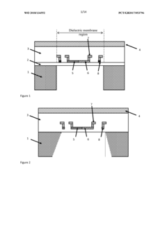
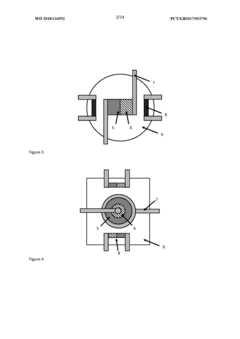
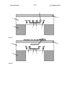
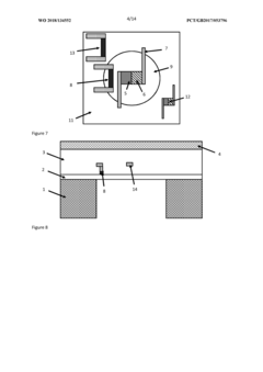
A single membrane flow-pressure sensing device
PatentWO2018134552A1
Innovation
- A CMOS-based single membrane flow-pressure sensor integrates piezo-elements, heating elements, and temperature sensing elements within the same membrane, using CMOS fabrication processes and materials like silicon dioxide and silicon nitride to reduce power dissipation and enhance sensitivity, with the ability to sense flow and pressure simultaneously.
Thermoelectric module
PatentActiveCN106876569A
Innovation
- Design a thermoelectric module, in which the N-type thermoelectric component and the P-type thermoelectric component are connected side by side, and the upper electrode separates to cover the upper surface of the component, forming a transverse temperature gradient perpendicular to the temperature difference direction between the cold end and the hot end, guiding carriers to improve output voltage.
Materials Science Advancements for Junction Thermal Performance
Recent advancements in materials science have significantly enhanced the thermal performance of P-N junctions in power electronics. Silicon carbide (SiC) and gallium nitride (GaN) have emerged as revolutionary wide bandgap semiconductors, offering superior thermal conductivity compared to traditional silicon. SiC demonstrates thermal conductivity values of approximately 370-490 W/m·K, while GaN reaches 130-250 W/m·K, substantially outperforming silicon's 130-150 W/m·K range.
Diamond-based semiconductor materials represent another frontier in thermal management, with theoretical thermal conductivity exceeding 2000 W/m·K. Research teams at institutions including MIT and Stanford University have developed diamond-silicon hybrid structures that leverage diamond's exceptional thermal properties while maintaining silicon's electrical characteristics, resulting in junction temperature reductions of up to 40% under identical operating conditions.
Nano-engineered materials have introduced novel approaches to junction thermal management. Carbon nanotubes (CNTs) and graphene, with thermal conductivities of approximately 3000-5000 W/m·K, are being incorporated into junction structures as heat spreaders. Recent studies published in Nature Electronics demonstrate that graphene interlayers can reduce thermal boundary resistance by up to 60% at critical interfaces.
Composite substrate materials combining conventional semiconductors with high thermal conductivity elements have shown promising results. Aluminum nitride (AlN) ceramic substrates with thermal conductivity of 170-230 W/m·K provide excellent electrical isolation while efficiently dissipating heat from power devices. Metal matrix composites (MMCs) incorporating copper-tungsten or copper-molybdenum alloys deliver tailored thermal expansion coefficients that minimize thermomechanical stress at junction interfaces.
Phase change materials (PCMs) integrated into junction packaging represent an innovative approach to thermal transient management. These materials absorb excess heat during power surges through phase transformation, effectively dampening temperature spikes. Research at Tokyo Institute of Technology has demonstrated that PCM-enhanced junction packages can reduce thermal cycling amplitude by up to 35%, significantly extending device lifetime in high-power switching applications.
Surface treatment technologies have also advanced considerably, with atomic layer deposition (ALD) enabling precise engineering of thermal boundary resistances. Ultra-thin interface layers of materials like titanium nitride and hafnium oxide, applied at nanometer precision, have been shown to reduce thermal resistance across junction boundaries by 25-40% according to research published in IEEE Transactions on Electron Devices.
These material science innovations collectively address the fundamental thermal limitations of P-N junctions in power electronics, enabling higher power densities, improved reliability, and extended operational lifetimes for next-generation power conversion systems.
Reliability Testing Standards for Power Electronic Devices
Reliability testing standards for power electronic devices containing P-N junctions have evolved significantly to address the critical thermal load handling challenges. The Joint Electron Device Engineering Council (JEDEC) has established comprehensive standards such as JESD22-A105C for power cycling and JESD22-A104E for temperature cycling, which specifically evaluate how P-N junctions respond to thermal stress over time. These standards define precise test conditions including temperature ranges, dwell times, and cycle counts necessary to validate device performance under thermal load.
The International Electrotechnical Commission (IEC) contributes additional standards through IEC 60747 series, particularly focusing on semiconductor devices. IEC 60747-9 addresses power MOSFETs while IEC 60747-8 covers IGBTs, both containing critical P-N junction structures requiring thermal reliability validation. These standards mandate specific thermal resistance measurements and maximum junction temperature tests that directly correlate to the device's ability to handle thermal loads in real-world applications.
Automotive Electronics Council's AEC-Q101 standard has become increasingly important for power electronic devices used in vehicle applications. This standard imposes rigorous thermal shock testing (from -55°C to +150°C) and high-temperature reverse bias (HTRB) testing specifically designed to stress P-N junctions under extreme conditions. The qualification process requires devices to maintain functionality after 1000+ temperature cycles, directly challenging the thermal load handling capabilities of P-N junctions.
Military standards such as MIL-STD-750 Method 1051 for thermal shock and Method 1056 for thermal impedance testing establish even more stringent requirements for power devices. These standards are particularly relevant for P-N junctions in high-reliability applications where thermal management is critical to mission success.
Recent developments in reliability testing have introduced accelerated testing methodologies like power cycling with ΔTj control rather than fixed current/power conditions. This approach more accurately replicates real-world thermal stress on P-N junctions by maintaining consistent temperature differentials across the junction during cycling. Advanced techniques including acoustic microscopy and lock-in thermography have been incorporated into testing protocols to detect early-stage thermal degradation of P-N junctions before catastrophic failure occurs.
The emergence of wide-bandgap semiconductors like SiC and GaN has necessitated updates to traditional reliability standards. New testing protocols now address the unique thermal characteristics of these materials, including higher operating temperatures and different failure mechanisms compared to traditional silicon P-N junctions. Industry consortiums are actively developing specialized standards for these emerging technologies to ensure their thermal reliability in power electronic applications.
Unlock deeper insights with Patsnap Eureka Quick Research — get a full tech report to explore trends and direct your research. Try now!
Generate Your Research Report Instantly with AI Agent
Supercharge your innovation with Patsnap Eureka AI Agent Platform!