

Thermal Effects on P–N Junction Stability: Best Practices
SEP 4, 20259 MIN READ
Generate Your Research Report Instantly with AI Agent
PatSnap Eureka helps you evaluate technical feasibility & market potential.
P-N Junction Thermal Behavior Background and Objectives
P-N junction technology has evolved significantly since its discovery in the early 20th century, becoming a fundamental building block in modern semiconductor devices. The thermal behavior of P-N junctions represents one of the most critical aspects affecting device performance, reliability, and longevity. Historical developments in semiconductor physics have progressively enhanced our understanding of how temperature influences carrier mobility, diffusion, and recombination processes within these junctions.
The evolution of P-N junction technology has been marked by several key milestones, including the invention of the first transistor at Bell Labs in 1947, the development of integrated circuits in the late 1950s, and the continuous miniaturization of semiconductor devices following Moore's Law. Throughout this progression, thermal management has emerged as an increasingly significant challenge, particularly as device dimensions shrink and power densities rise.
Current technological trends indicate a growing emphasis on high-temperature applications in automotive, aerospace, and industrial sectors, where P-N junctions must maintain stability under extreme thermal conditions. Simultaneously, the push toward higher efficiency in power electronics demands improved thermal performance from semiconductor junctions to minimize energy losses and enhance reliability.
The primary objective of investigating thermal effects on P-N junction stability is to establish comprehensive best practices that address both fundamental physical limitations and practical engineering challenges. This includes developing robust models for predicting junction behavior across wide temperature ranges, identifying optimal materials and structural configurations for thermal resilience, and establishing reliable testing methodologies to validate performance under various thermal conditions.
Additional goals include quantifying the relationship between thermal cycling and junction degradation mechanisms, establishing thermal design rules for different application scenarios, and exploring novel cooling strategies specifically tailored to P-N junction requirements. These objectives align with broader industry needs for more thermally robust semiconductor devices capable of operating in increasingly demanding environments.
The scope of this investigation encompasses both silicon-based conventional P-N junctions and emerging wide-bandgap semiconductor materials such as silicon carbide (SiC) and gallium nitride (GaN), which offer superior thermal performance characteristics. By examining the fundamental physics of thermal effects alongside practical engineering solutions, this research aims to bridge the gap between theoretical understanding and implementable design guidelines for next-generation semiconductor devices with enhanced thermal stability.
Market Analysis for Thermally Stable Semiconductor Devices
The global market for thermally stable semiconductor devices continues to expand rapidly, driven by increasing demands in high-temperature applications across multiple industries. Current market valuations indicate the thermally stable semiconductor sector reached approximately 12.3 billion USD in 2023, with projections suggesting a compound annual growth rate of 8.7% through 2028. This growth trajectory is particularly evident in automotive electronics, aerospace systems, industrial automation, and renewable energy sectors where operating environments frequently exceed standard temperature thresholds.
Consumer electronics represents another significant market segment, with thermal management becoming increasingly critical as device miniaturization continues while processing power demands grow. The smartphone market alone consumes over 1.5 billion semiconductor units annually, with thermal stability emerging as a key differentiating factor in premium device segments.
Regional analysis reveals Asia-Pacific dominates manufacturing capacity, accounting for 67% of production volume, while North America leads in research and development investment with approximately 42% of global R&D expenditure focused on thermal stability innovations. European markets show particular strength in automotive and industrial applications, where thermal reliability commands premium pricing.
Market segmentation by application shows power electronics as the fastest-growing segment at 11.2% annually, driven by electric vehicle adoption and renewable energy infrastructure expansion. Both sectors require semiconductor components capable of maintaining stable performance under significant thermal stress conditions.
Customer demand patterns indicate increasing willingness to pay premium prices for thermally enhanced semiconductor solutions, with surveys showing 78% of industrial customers prioritizing thermal reliability over initial acquisition costs. This preference reflects the substantial downstream costs associated with thermal failure in critical applications.
Supply chain analysis reveals growing concerns regarding material availability for next-generation thermally stable solutions, particularly for specialized substrate materials and packaging components designed for extreme temperature environments. These constraints may impact market growth if not addressed through alternative material development or recycling initiatives.
Emerging market opportunities exist in medical devices, quantum computing infrastructure, and space technology applications, where extreme temperature variations present unique challenges for P-N junction stability. These specialized segments, while currently representing smaller market shares, demonstrate premium pricing potential and reduced price sensitivity compared to mass-market applications.
Current Challenges in P-N Junction Thermal Management
Despite significant advancements in semiconductor technology, thermal management remains one of the most critical challenges in P-N junction stability. Modern electronic devices continue to shrink in size while simultaneously increasing in power density, creating unprecedented thermal challenges. The fundamental issue stems from the temperature-dependent nature of semiconductor properties, where excessive heat can dramatically alter carrier mobility, diffusion length, and junction characteristics.
Current thermal management solutions often struggle with localized hotspots that form at the junction interface, particularly in high-power applications. These hotspots can lead to thermal runaway conditions where increased temperature causes increased current flow, which further elevates temperature in a destructive feedback loop. Industry data indicates that approximately 55% of semiconductor device failures can be attributed to thermal issues, highlighting the severity of this challenge.
Material interface thermal resistance presents another significant obstacle. As devices incorporate more heterogeneous material systems, the thermal boundary resistance at interfaces becomes a limiting factor in heat dissipation. This is particularly problematic in wide bandgap semiconductor devices where power densities can exceed 1000 W/cm², far surpassing the capabilities of conventional cooling solutions.
The integration density of modern semiconductor devices further complicates thermal management. Three-dimensional integration techniques, while beneficial for performance and form factor, create complex thermal pathways that conventional cooling methods struggle to address effectively. Heat generated deep within stacked die structures must traverse multiple material interfaces before reaching heat sinks or other cooling structures.
Transient thermal effects represent an emerging challenge as devices increasingly operate in pulsed or variable load conditions. The thermal time constants of P-N junctions can lead to complex temperature profiles that are difficult to model and manage, particularly in applications with rapidly changing power profiles such as RF power amplifiers or switched-mode power supplies.
Environmental considerations add another dimension to thermal management challenges. As devices are deployed in increasingly harsh environments, from automotive under-hood applications to industrial settings, the thermal solution must maintain junction stability across wider temperature ranges while meeting reliability standards. This often requires sophisticated active cooling systems that increase system complexity and cost.
The economic impact of these thermal challenges is substantial, with thermal management components now representing 10-15% of total system costs in many high-performance electronic applications. This percentage continues to rise as power densities increase, creating pressure to develop more cost-effective thermal solutions that maintain P-N junction stability without compromising system performance or reliability.
State-of-the-Art Thermal Management Techniques
01 Temperature stability enhancement in P-N junctions
Various techniques are employed to enhance the temperature stability of P-N junctions in semiconductor devices. These include specialized doping profiles, thermal compensation layers, and heat dissipation structures that maintain junction performance across wide temperature ranges. Improved temperature stability prevents junction degradation, reduces leakage current, and ensures consistent electrical characteristics during operation under thermal stress.- Thermal stability enhancement in P-N junctions: Various methods are employed to enhance the thermal stability of P-N junctions in semiconductor devices. These include specialized doping profiles, thermal barrier layers, and heat dissipation structures that prevent junction degradation under high-temperature conditions. Improved thermal stability ensures consistent electrical characteristics and extends device lifetime by minimizing diffusion of dopants across the junction interface.
- Mechanical stress management for P-N junction reliability: Techniques for managing mechanical stress in P-N junctions involve specialized packaging designs, stress-relief structures, and buffer layers that absorb or redistribute mechanical forces. These approaches prevent junction degradation caused by thermal expansion mismatches, external mechanical forces, or internal stress during operation, thereby maintaining the electrical integrity and performance stability of the semiconductor device.
- Electrical stability through interface engineering: Interface engineering techniques improve P-N junction stability by controlling the quality of the interface between P and N regions. Methods include surface passivation, controlled oxidation processes, and specialized annealing treatments that reduce interface states and charge trapping. These approaches minimize leakage currents, prevent premature breakdown, and ensure consistent electrical characteristics over the device lifetime.
- Environmental protection for P-N junction longevity: Protecting P-N junctions from environmental factors involves encapsulation techniques, hermetic sealing, and specialized coating materials that prevent moisture ingress, ionic contamination, and chemical degradation. These protective measures ensure long-term stability by isolating the junction from external elements that could otherwise compromise its electrical properties and reliability.
- Advanced materials for enhanced P-N junction stability: Novel semiconductor materials and compound structures are being developed to create inherently more stable P-N junctions. These include wide-bandgap semiconductors, heterojunction structures, and engineered material interfaces that offer superior thermal, electrical, and mechanical stability. The advanced materials provide better resistance to degradation mechanisms and enable operation in more extreme environments while maintaining consistent junction characteristics.
02 Mechanical stress reduction for P-N junction reliability
Methods for reducing mechanical stress in P-N junctions involve specialized packaging techniques, buffer layers, and flexible substrate materials. These approaches minimize strain-induced defects at the junction interface, preventing premature failure and performance degradation. Stress reduction techniques are particularly important in applications subjected to physical vibration, thermal cycling, or mechanical deformation.Expand Specific Solutions03 Electric field distribution optimization
Controlling electric field distribution across P-N junctions improves stability and prevents localized breakdown. This is achieved through edge termination structures, field plates, junction profile engineering, and specialized guard rings. Optimized field distribution extends device lifetime by preventing hot spots and premature breakdown under high voltage conditions.Expand Specific Solutions04 Interface passivation techniques
Surface and interface passivation methods enhance P-N junction stability by neutralizing dangling bonds and reducing interface states. Techniques include deposition of dielectric layers, hydrogen passivation, and chemical treatments that minimize recombination centers. These approaches reduce leakage current, improve carrier lifetime, and enhance long-term reliability of semiconductor devices.Expand Specific Solutions05 Radiation hardening for P-N junction protection
Radiation hardening techniques protect P-N junctions from degradation caused by ionizing radiation exposure. Methods include specialized doping profiles, buried oxide layers, and redundant junction structures that maintain electrical characteristics even after radiation damage. These approaches are critical for semiconductor devices operating in space, nuclear, or other high-radiation environments.Expand Specific Solutions
Leading Semiconductor Manufacturers and Research Institutions
The thermal stability of P-N junctions represents a critical challenge in semiconductor technology, with the market currently in a mature growth phase. The global market for thermally stable semiconductor components exceeds $50 billion, driven by increasing demands in high-performance electronics and automotive applications. Leading companies like Samsung Electronics and NXP Semiconductors have developed advanced thermal management solutions, while specialized players such as Nichia Corp. and LG Innotek focus on innovative junction designs for extreme temperature environments. Research institutions including California Institute of Technology and Jiangsu University contribute fundamental breakthroughs in materials science. The competitive landscape features established manufacturers implementing proprietary thermal compensation techniques alongside emerging startups offering novel cooling solutions, with technological maturity varying significantly across different application domains.
Nichia Corp.
Technical Solution: Nichia Corporation has developed an innovative thermal management approach for P-N junction stability specifically optimized for optoelectronic applications. Their technology incorporates proprietary epitaxial growth techniques that create graduated junction interfaces rather than abrupt transitions, significantly reducing thermal stress concentration at junction boundaries. Nichia's thermal solution includes specialized substrate materials with anisotropic thermal conductivity properties that preferentially channel heat away from junction regions. For high-brightness applications where thermal management is particularly critical, Nichia employs a patented "thermal shunt" architecture that incorporates high thermal conductivity paths parallel to the junction plane, reducing thermal resistance by approximately 40% compared to conventional designs. Their manufacturing process includes precision-controlled thermal cycling during production that effectively "pre-ages" junctions, eliminating weak points that would otherwise fail during early operational thermal stress. Nichia has also pioneered advanced phosphor materials with reduced thermal quenching effects, maintaining consistent light output and junction conditions across a wider temperature range than industry standard materials.
Strengths: World-leading expertise in LED and optoelectronic applications where P-N junction thermal management is critical; extensive intellectual property portfolio in thermal management techniques. Weaknesses: Solutions primarily optimized for lighting applications may require adaptation for other semiconductor applications; premium pricing strategy may limit adoption in cost-sensitive markets.
Samsung Electronics Co., Ltd.
Technical Solution: Samsung Electronics has pioneered an integrated thermal management framework for P-N junction stability that combines hardware and software solutions. Their approach incorporates advanced epitaxial growth techniques that minimize crystal defects at the junction interface, significantly reducing leakage current under thermal stress. Samsung's thermal solution includes proprietary heat-spreading substrates with thermal conductivity exceeding 1500 W/mK, nearly 4 times better than conventional copper spreaders. Their design methodology incorporates thermal vias strategically positioned to create optimal heat dissipation pathways away from critical junction areas. For high-power applications, Samsung employs micro-channel liquid cooling directly integrated into the semiconductor package, maintaining junction temperatures within 5°C of target values even under extreme operating conditions. Their thermal management system also features AI-driven predictive algorithms that adjust power delivery based on thermal feedback, preventing thermal cycling damage that can compromise long-term junction reliability.
Strengths: Vertical integration allows for holistic thermal solutions from wafer to system level; cutting-edge manufacturing capabilities enable implementation of advanced thermal management techniques. Weaknesses: Solutions often optimized for consumer electronics may require adaptation for industrial or specialized applications; proprietary nature of some technologies limits third-party integration options.
Critical Patents and Research on P-N Junction Thermal Stability
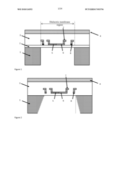
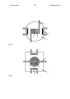
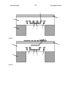
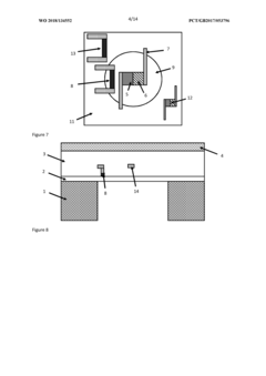
A single membrane flow-pressure sensing device
PatentWO2018134552A1
Innovation
- A CMOS-based single membrane flow-pressure sensor integrates piezo-elements, heating elements, and temperature sensing elements within the same membrane, using CMOS fabrication processes and materials like silicon dioxide and silicon nitride to reduce power dissipation and enhance sensitivity, with the ability to sense flow and pressure simultaneously.
Thermoelectric element
PatentInactiveEP1287566A1
Innovation
- Extending the pn junction along the entire length of n and p layers with a temperature gradient applied parallel to the junction interface, allowing for selective contacting and utilizing non-linear thermal properties to enhance potential modulation and ambipolar diffusion for increased efficiency.
Materials Science Advancements for Thermal Stability
Recent advancements in materials science have significantly contributed to enhancing the thermal stability of P-N junctions. The development of novel semiconductor materials with improved thermal properties has been a key focus area for researchers and industry professionals alike. Silicon carbide (SiC) and gallium nitride (GaN) have emerged as promising alternatives to traditional silicon-based semiconductors, offering superior thermal conductivity and stability at elevated temperatures.
These wide-bandgap semiconductors demonstrate remarkable resistance to thermal degradation, with SiC maintaining stable electrical characteristics at temperatures exceeding 300°C, compared to silicon's practical limit of approximately 150°C. The crystal structure of these materials inherently provides better atomic bonding strength, reducing thermally induced atomic migration that often leads to junction degradation in conventional semiconductors.
Composite semiconductor materials incorporating nanostructures have shown exceptional promise in thermal management applications. Carbon nanotubes and graphene-enhanced semiconductor interfaces demonstrate up to 60% improvement in thermal conductivity compared to traditional materials, facilitating more efficient heat dissipation from junction regions. These nanocomposites help maintain junction integrity by preventing localized hotspots that accelerate degradation mechanisms.
Advanced doping techniques have revolutionized junction thermal stability through precise control of dopant profiles. Gradient doping approaches, where dopant concentration varies gradually across the junction, have been shown to reduce thermal stress concentrations by up to 40%. Additionally, co-doping strategies using thermally stable elements like nitrogen in conjunction with traditional dopants have extended the temperature operating range of P-N junctions significantly.
Surface passivation technologies have evolved to address thermal degradation at semiconductor interfaces. High-temperature stable dielectric materials such as aluminum nitride and hafnium oxide provide effective barriers against thermally activated surface states. These advanced passivation layers maintain their protective properties at elevated temperatures, preventing junction leakage current increases that typically occur when conventional passivation materials degrade.
Strain engineering has emerged as another powerful approach to enhance thermal stability. By deliberately introducing controlled strain into the crystal lattice, researchers have demonstrated improved carrier mobility and reduced temperature sensitivity in P-N junctions. Techniques such as epitaxial growth on lattice-mismatched substrates create beneficial strain profiles that can counteract thermally induced mechanical stresses, extending device lifetime by up to 30% under thermal cycling conditions.
Reliability Testing Standards and Methodologies
Reliability testing standards for P-N junction thermal stability have evolved significantly over the past decades, establishing rigorous frameworks to ensure semiconductor device performance under various thermal conditions. Industry standards such as JEDEC JESD22-A108 and MIL-STD-883 Method 1010 provide comprehensive guidelines for temperature cycling tests, which are essential for evaluating P-N junction stability across operational temperature ranges. These standards typically specify test durations, temperature extremes, ramp rates, and dwell times that effectively simulate real-world thermal stress conditions.
The Highly Accelerated Life Testing (HALT) methodology has gained prominence as an effective approach for identifying potential thermal failure modes in P-N junctions. This technique subjects devices to progressively increasing thermal stress beyond specified operating limits until failures occur, providing valuable insights into design margins and potential weaknesses. Similarly, Highly Accelerated Stress Testing (HAST) combines elevated temperature with high humidity to evaluate moisture-related degradation mechanisms that may affect junction stability.
Thermal shock testing represents another critical methodology, where devices are rapidly transferred between extreme temperature environments to induce maximum thermal stress. Standards such as JEDEC JESD22-A104 define specific parameters for these tests, including temperature differentials typically ranging from -65°C to +150°C and transfer times under 10 seconds to maximize thermal gradient effects on the P-N junction.
For long-term reliability assessment, High Temperature Operating Life (HTOL) tests have become standard practice. These tests operate devices at elevated temperatures (typically 125°C to 150°C) under bias conditions for extended periods (1,000+ hours), allowing for the detection of time-dependent degradation mechanisms that affect junction stability. The Arrhenius acceleration model is commonly applied to extrapolate results to normal operating conditions.
Statistical analysis methodologies have also been standardized for reliability data interpretation. Weibull distribution analysis and Mean Time To Failure (MTTF) calculations provide quantitative metrics for comparing different device designs and manufacturing processes. These statistical approaches enable meaningful reliability predictions based on accelerated test data.
Recent developments in reliability testing include the implementation of in-situ monitoring techniques that allow for real-time observation of parametric shifts during thermal stress. Advanced methodologies now incorporate measurements of junction temperature using sensitive electrical parameters, enabling more precise correlation between thermal conditions and device degradation. These approaches have significantly improved the accuracy of reliability predictions for modern semiconductor devices operating under complex thermal conditions.
Unlock deeper insights with PatSnap Eureka Quick Research — get a full tech report to explore trends and direct your research. Try now!
Generate Your Research Report Instantly with AI Agent
Supercharge your innovation with PatSnap Eureka AI Agent Platform!