

Benchmark P–N Junctions: Conductivity and Energy Conversion
SEP 4, 20259 MIN READ
Generate Your Research Report Instantly with AI Agent
PatSnap Eureka helps you evaluate technical feasibility & market potential.
P-N Junction Technology Background and Objectives
P-N junctions represent one of the most fundamental structures in semiconductor technology, serving as the building blocks for numerous electronic devices since their theoretical conception in the early 20th century. The evolution of P-N junction technology has been closely intertwined with the broader development of semiconductor physics, beginning with the pioneering work of scientists like Walter Brattain, John Bardeen, and William Shockley in the 1940s, which led to the invention of the transistor and subsequently earned them the Nobel Prize in Physics.
The technological trajectory of P-N junctions has been characterized by continuous refinement in fabrication techniques, material science advancements, and theoretical understanding. From the initial germanium-based junctions to the widespread adoption of silicon, and now extending to compound semiconductors and emerging materials like gallium nitride and silicon carbide, each evolutionary step has expanded the application scope and performance capabilities of these critical components.
Current research in P-N junction technology is increasingly focused on optimizing conductivity properties and enhancing energy conversion efficiency. This dual focus reflects the growing importance of semiconductor devices in both information processing technologies and sustainable energy solutions. The conductivity characteristics of P-N junctions directly impact the performance of electronic devices, while their energy conversion capabilities are central to photovoltaic cells, thermoelectric generators, and other renewable energy technologies.
The primary technical objectives in this field include developing P-N junctions with reduced resistance, minimized leakage current, enhanced carrier mobility, and improved thermal stability. For energy conversion applications, key goals involve increasing the photon-to-electron conversion efficiency, broadening the spectral response range, and extending operational lifetimes under various environmental conditions.
Benchmark studies of P-N junctions are essential for establishing standardized performance metrics, enabling meaningful comparisons across different material systems and fabrication methodologies. These benchmarks typically evaluate parameters such as forward voltage drop, reverse breakdown voltage, switching speed, temperature coefficient, and quantum efficiency in energy conversion contexts.
The technological objectives extend beyond mere performance enhancement to address manufacturing scalability, cost reduction, and environmental sustainability. As semiconductor devices become increasingly ubiquitous in global infrastructure, ensuring that P-N junction technology can be produced efficiently, economically, and with minimal environmental impact becomes paramount for continued industry growth and technological adoption.
Market Applications of P-N Junction Devices
P-N junction devices have revolutionized numerous industries through their fundamental ability to control electrical current flow and convert energy. The global semiconductor market, where P-N junctions serve as building blocks, reached approximately $573 billion in 2022 and continues to grow steadily at around 8% annually, underscoring the economic significance of these devices.
The photovoltaic industry represents one of the largest applications of P-N junction technology. Solar cells, which fundamentally rely on P-N junctions to convert sunlight into electricity, have seen dramatic market expansion. The global solar energy market surpassed $180 billion in 2021, with projections indicating continued growth as renewable energy adoption accelerates worldwide. Efficiency improvements in P-N junction design have directly contributed to reducing the levelized cost of solar electricity by over 85% in the past decade.
In electronics and computing, P-N junction-based diodes and transistors form the foundation of modern digital infrastructure. The global semiconductor device market specifically related to P-N junction components exceeds $100 billion annually. These components enable everything from consumer electronics to data centers that power cloud computing and artificial intelligence applications.
The telecommunications sector heavily relies on P-N junction devices for signal processing, amplification, and optical communication. Photodiodes and laser diodes, both P-N junction-based technologies, are crucial components in fiber optic networks that form the backbone of global internet infrastructure. This market segment alone represents approximately $75 billion globally.
Power electronics applications leverage P-N junctions in devices like power diodes, thyristors, and insulated-gate bipolar transistors (IGBTs). These components are essential for electric vehicle powertrains, renewable energy inverters, and industrial motor controls. The power semiconductor market exceeded $40 billion in 2021 with projected growth rates of 9-10% annually through 2028.
The medical technology sector utilizes P-N junction devices in diagnostic equipment, therapeutic devices, and monitoring systems. From LED-based phototherapy devices to radiation detectors in imaging equipment, these applications represent a specialized but high-value market segment worth approximately $15 billion.
Emerging applications include quantum computing, where specialized P-N junction structures are being explored for qubit implementation, and neuromorphic computing, where P-N junction-based memristors may enable brain-inspired computing architectures. While currently smaller markets, these applications represent potential high-growth areas for advanced P-N junction technologies in the coming decades.
Current P-N Junction Challenges and Limitations
Despite significant advancements in semiconductor technology, P-N junctions face several critical challenges that limit their performance in both conductivity and energy conversion applications. One of the most persistent issues is the recombination of charge carriers at the junction interface, which reduces efficiency in photovoltaic cells and other energy conversion devices. This recombination occurs primarily due to defects, impurities, and crystallographic imperfections that create energy states within the bandgap, acting as recombination centers.
Temperature sensitivity represents another significant limitation, as P-N junction performance degrades substantially at elevated temperatures. This thermal instability manifests through increased leakage current, reduced carrier mobility, and altered bandgap characteristics, making these devices less reliable in high-temperature environments common in industrial applications and certain geographic regions.
The physical scaling constraints of P-N junctions have become increasingly problematic as devices continue to miniaturize. At nanoscale dimensions, quantum tunneling effects become pronounced, leading to increased leakage currents and reduced rectification ratios. Additionally, as junction dimensions decrease, surface effects become dominant over bulk properties, introducing variability in device performance.
Material limitations also present significant challenges. Traditional silicon-based P-N junctions approach their theoretical efficiency limits, particularly in photovoltaic applications where the Shockley-Queisser limit restricts single-junction solar cell efficiency to approximately 33%. While alternative materials such as III-V semiconductors offer improved performance, they introduce manufacturing complexity and substantially higher costs.
Manufacturing consistency remains problematic, particularly for large-area applications like solar panels. Achieving uniform doping profiles and junction characteristics across large substrates continues to challenge production processes, resulting in performance variations and reduced yield rates.
Power loss through parasitic resistances significantly impacts energy conversion efficiency. Series resistance from contacts, semiconductor bulk, and junction regions, combined with shunt resistance from manufacturing defects, creates power dissipation pathways that reduce overall device performance.
Finally, radiation damage presents a critical limitation for P-N junctions in aerospace, nuclear, and certain industrial applications. High-energy particles can create displacement damage and ionization effects that permanently degrade junction characteristics, necessitating radiation-hardening techniques that often compromise other performance parameters.
Benchmark Methodologies for P-N Junction Performance
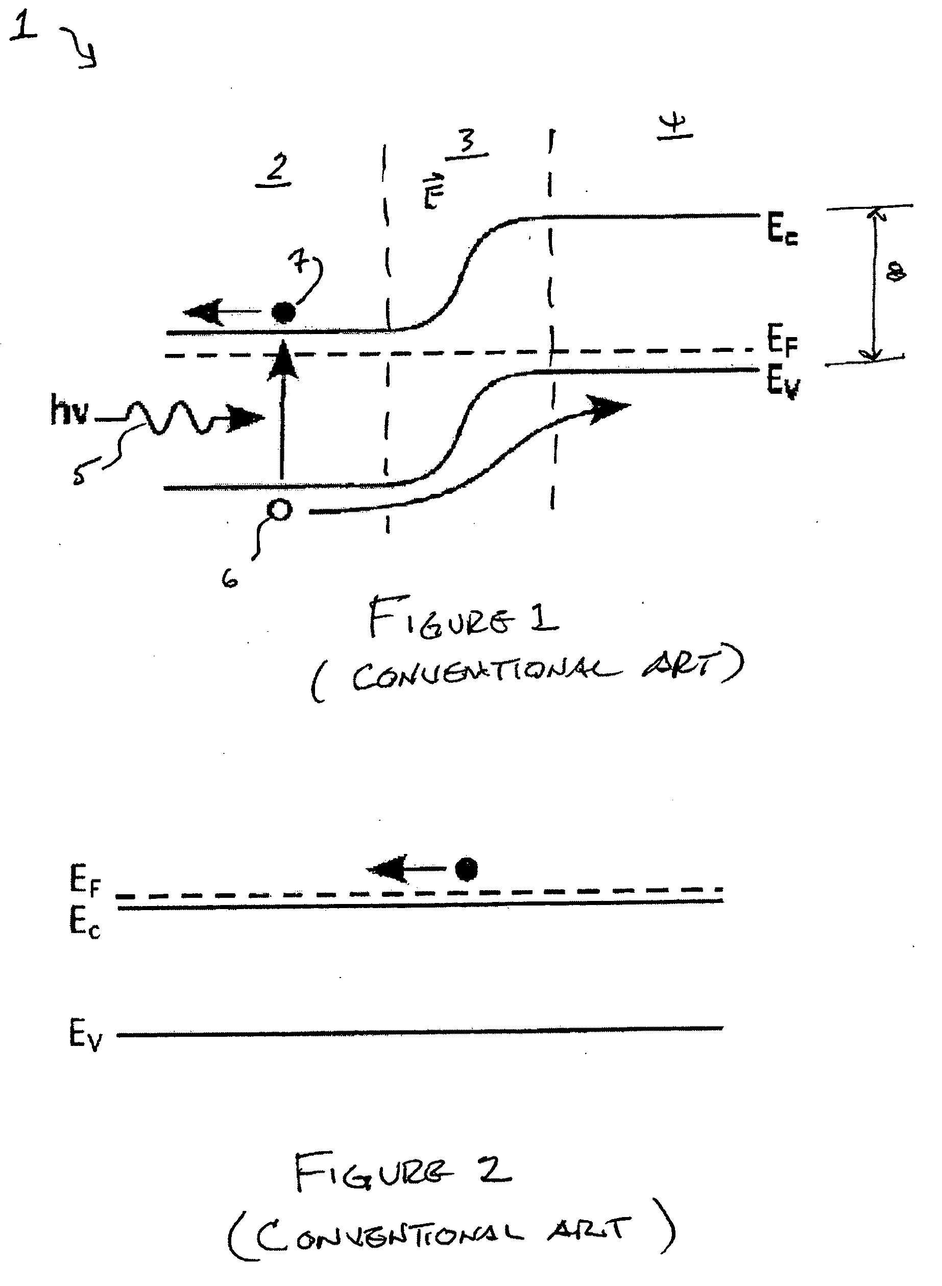
01 Basic principles of P-N junction conductivity
P-N junctions are fundamental semiconductor structures formed by joining P-type and N-type semiconductor materials. The conductivity at these junctions is governed by the movement of charge carriers (electrons and holes) across the depletion region. When forward biased, majority carriers can cross the junction, allowing current flow. Under reverse bias, the depletion region widens, limiting conductivity. These principles form the basis for various semiconductor devices including diodes and transistors.- Basic principles of P-N junction conductivity: P-N junctions form the fundamental building blocks of semiconductor devices. The conductivity at these junctions is determined by the interaction between p-type (hole-rich) and n-type (electron-rich) semiconductor materials. When these materials are brought together, a depletion region forms at the junction, creating an electric field that affects the flow of charge carriers. Understanding these basic principles is essential for designing and optimizing semiconductor devices.
- Methods to enhance P-N junction conductivity: Various techniques can be employed to enhance the conductivity of P-N junctions. These include doping optimization, junction engineering, and thermal treatments. By carefully controlling the concentration and distribution of dopants, the electrical properties of the junction can be tailored for specific applications. Additionally, post-fabrication treatments such as annealing can improve junction quality by reducing defects and enhancing carrier mobility.
- Advanced P-N junction structures for improved conductivity: Advanced P-N junction structures have been developed to achieve superior conductivity characteristics. These include heterojunctions, graded junctions, and multi-layer structures. By engineering the junction profile and incorporating novel materials, these advanced structures can overcome limitations of conventional P-N junctions. Such innovations enable enhanced carrier transport, reduced resistance, and improved overall device performance.
- Fabrication techniques for high-conductivity P-N junctions: Specialized fabrication techniques are crucial for creating high-conductivity P-N junctions. These include epitaxial growth, ion implantation, diffusion processes, and advanced lithography. The precise control of junction formation parameters significantly impacts the resulting electrical characteristics. Modern semiconductor manufacturing employs sophisticated processes to achieve atomically sharp interfaces, optimal doping profiles, and minimal defect densities, all of which contribute to enhanced junction conductivity.
- Measurement and characterization of P-N junction conductivity: Accurate measurement and characterization of P-N junction conductivity are essential for device development and quality control. Various techniques including current-voltage (I-V) characterization, capacitance-voltage (C-V) profiling, and conductance measurements provide insights into junction properties. Advanced analytical methods such as scanning probe microscopy and impedance spectroscopy allow for nanoscale evaluation of conductivity variations across the junction. These measurements help optimize junction design and fabrication processes.
02 Methods to enhance P-N junction conductivity
Various techniques can be employed to enhance the conductivity of P-N junctions. These include doping optimization to control carrier concentration, junction engineering to reduce defects, surface treatment to minimize recombination, and thermal annealing processes to improve crystal quality. Advanced fabrication methods can create more efficient junctions with higher conductivity, leading to improved device performance in electronic applications.Expand Specific Solutions03 Novel materials for improved P-N junction performance
Research into novel materials has led to significant improvements in P-N junction conductivity. These include compound semiconductors, wide bandgap materials, organic semiconductors, and two-dimensional materials. These advanced materials offer unique electrical properties that can be exploited to create junctions with superior conductivity characteristics, enabling higher efficiency and performance in electronic and optoelectronic devices.Expand Specific Solutions04 Testing and measurement of P-N junction conductivity
Accurate measurement of P-N junction conductivity is essential for device characterization and quality control. Various techniques are employed including current-voltage (I-V) characterization, capacitance-voltage profiling, four-point probe measurements, and scanning probe microscopy. Advanced testing methods allow for precise determination of junction properties at different operating conditions, enabling optimization of device performance and reliability.Expand Specific Solutions05 Applications leveraging P-N junction conductivity properties
The unique conductivity properties of P-N junctions are leveraged in numerous applications. These include solar cells where the junction converts light to electrical energy, power electronics utilizing controlled conductivity for switching, memory devices exploiting junction characteristics for data storage, and sensors that detect environmental changes through conductivity variations. The versatility of P-N junctions makes them fundamental building blocks in modern electronic and optoelectronic systems.Expand Specific Solutions
Leading Companies and Research Institutions in Semiconductor Industry
The P-N junction technology market is currently in a growth phase, characterized by increasing applications in energy conversion and semiconductor devices. The market size is expanding rapidly due to rising demand for efficient power electronics and renewable energy solutions. Technologically, companies like Sharp Corp., Samsung Electronics, and Toyota Motor Corp. are leading innovation with advanced semiconductor manufacturing capabilities, while research institutions such as California Institute of Technology and University of North Carolina at Chapel Hill contribute fundamental breakthroughs. Nexperia BV and STMicroelectronics demonstrate maturity in commercial applications, particularly in power semiconductors. The competitive landscape shows a blend of established electronics manufacturers and specialized semiconductor companies developing next-generation junction technologies for improved conductivity and energy conversion efficiency.
STMicroelectronics (Rousset) SAS
Technical Solution: STMicroelectronics has developed benchmark P-N junction technology focusing on power semiconductor applications with enhanced conductivity characteristics. Their approach involves precision-engineered junction profiles using advanced ion implantation and thermal diffusion processes to create optimal doping gradients. ST's technology incorporates innovative buffer layer structures between the P and N regions to manage electric field distribution and improve breakdown voltage while maintaining low on-resistance. They have pioneered the implementation of super-junction architectures that fundamentally alter the conductivity-breakdown voltage trade-off in power devices. Their research demonstrates significant improvements in energy conversion efficiency, with their latest silicon carbide (SiC) P-N junction devices achieving up to 40% reduction in switching losses compared to conventional silicon technologies. ST has also developed specialized junction termination techniques to enhance reliability and performance consistency across temperature variations, critical for automotive and industrial applications.
Strengths: ST's expertise in wide bandgap semiconductors (SiC, GaN) provides advantages in high-temperature, high-power applications. Their established manufacturing capabilities ensure consistent quality and reliability. Weaknesses: Higher production costs compared to conventional silicon technologies may limit market penetration in cost-sensitive applications.
Samsung Electronics Co., Ltd.
Technical Solution: Samsung Electronics has developed advanced P-N junction technology for their semiconductor devices, focusing on enhancing conductivity and energy conversion efficiency. Their approach involves precise doping control and novel junction architectures to minimize carrier recombination losses. Samsung has pioneered the implementation of heterojunction structures with optimized band alignment to improve charge carrier separation and collection. Their research includes the development of tunnel junctions with high conductivity for multi-junction solar cells, achieving conversion efficiencies exceeding 22% in production cells. Samsung has also implemented advanced surface passivation techniques to reduce interface recombination, significantly improving device performance. Their benchmark P-N junction technology incorporates nanoscale engineering to enhance carrier mobility and reduce resistance at the junction interface, resulting in devices with superior electrical characteristics and energy conversion capabilities.
Strengths: Samsung's extensive manufacturing infrastructure allows for rapid scaling of new junction technologies. Their vertical integration enables optimization across the entire device stack. Weaknesses: Their proprietary technologies may limit broader industry adoption, and their focus on consumer electronics may constrain application in specialized energy conversion fields.
Key Patents and Research on P-N Junction Conductivity
Semiconductor device and method
PatentActiveUS20100230720A1
Innovation
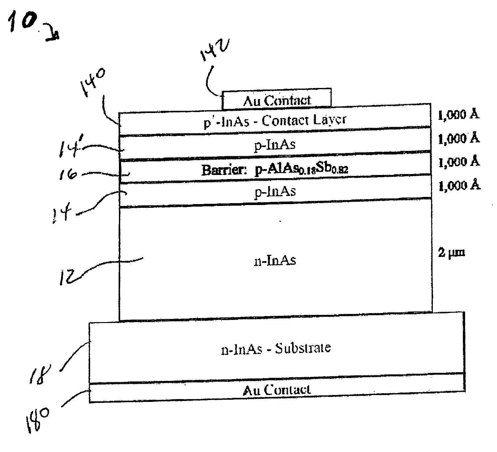
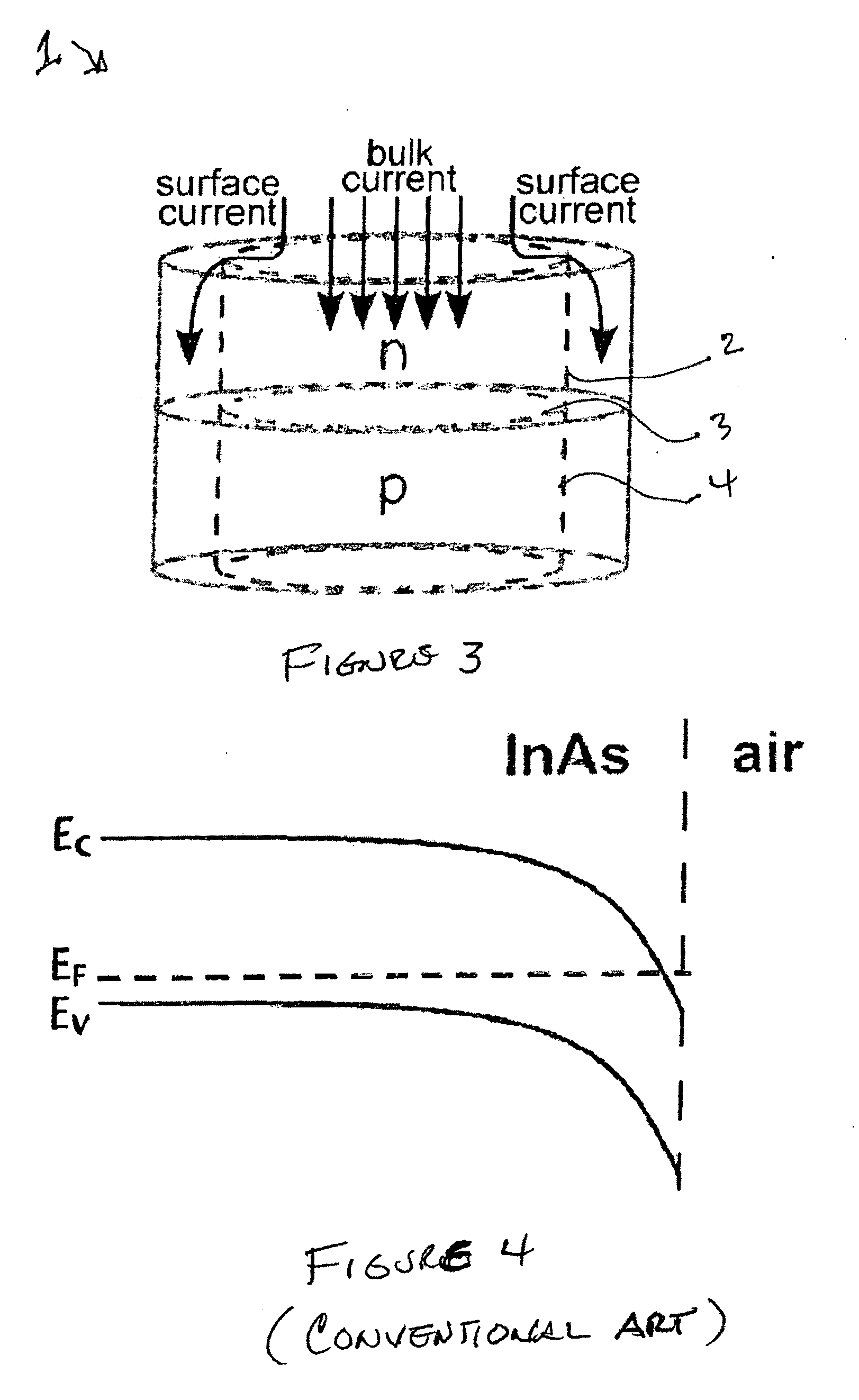
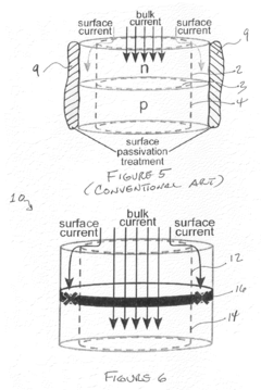
- The integration of unipolar barriers within the epitaxial structure of semiconductor devices during manufacturing, which blocks surface leakage currents while allowing bulk photocurrents to pass, eliminating the need for ex situ surface passivation treatments.
Power source and method of forming same
PatentActiveUS20190267503A1
Innovation
- A power source design that includes a substrate with a structured surface, radioactive material, particle converting material, and a photovoltaic device, where radiation particles are converted into electromagnetic radiation and then into electrical energy, utilizing a two-step process for high efficiency and longevity.
Materials Science Advancements for Enhanced P-N Junctions
Recent advancements in materials science have significantly enhanced the performance of P-N junctions, revolutionizing semiconductor technology and energy conversion applications. Novel materials with tailored band gaps and improved carrier mobility have emerged as game-changers in this field. These innovations address longstanding challenges related to efficiency limitations, thermal stability, and manufacturing scalability.
Nanostructured materials represent a particularly promising frontier, with quantum dots, nanowires, and two-dimensional materials demonstrating exceptional electronic properties when incorporated into junction designs. Silicon remains the industry standard, but compound semiconductors such as gallium arsenide (GaAs), gallium nitride (GaN), and silicon carbide (SiC) have shown remarkable improvements in conductivity parameters and energy conversion efficiency.
Perovskite materials have emerged as revolutionary candidates for next-generation P-N junctions, offering tunable bandgaps and excellent absorption coefficients. Their integration with traditional semiconductors in tandem structures has pushed conversion efficiencies beyond theoretical limits of single-junction devices. However, stability and durability concerns remain significant barriers to widespread commercial adoption.
Interface engineering has become a critical focus area, with atomic-level precision in material deposition enabling unprecedented control over junction properties. Advanced techniques such as atomic layer deposition (ALD) and molecular beam epitaxy (MBE) allow for precise manipulation of interface states, reducing recombination losses and enhancing overall performance metrics.
Doping innovations have similarly transformed junction capabilities, with techniques like delta-doping and selective area doping enabling more precise control over carrier concentrations. These approaches have minimized parasitic resistance while optimizing built-in electric fields across the junction, directly improving both conductivity and energy conversion parameters.
Flexible and stretchable semiconductor materials represent another significant advancement, opening new application domains for P-N junctions in wearable electronics and biointegrated systems. These materials maintain functional electronic properties under mechanical deformation, addressing limitations of traditional rigid semiconductor substrates.
Computational materials science has accelerated discovery through high-throughput screening and machine learning approaches, identifying promising material combinations with optimal properties for specific applications. This data-driven approach has significantly reduced development timelines and expanded the materials palette available for junction engineering.
Environmental Impact of P-N Junction Manufacturing Processes
The manufacturing processes of P-N junctions involve several environmentally significant aspects that warrant careful consideration. Traditional semiconductor fabrication techniques utilize substantial quantities of hazardous chemicals, including hydrofluoric acid, sulfuric acid, and various heavy metals, which pose significant environmental risks if improperly managed. The disposal of these chemicals requires specialized treatment facilities and protocols to prevent contamination of soil and water resources.
Energy consumption represents another critical environmental concern in P-N junction production. The high-temperature processes required for silicon purification, wafer production, and dopant diffusion consume considerable electrical power, contributing to carbon emissions when non-renewable energy sources are utilized. Recent industry analyses indicate that manufacturing a single six-inch silicon wafer can require up to 2,000 kilowatt-hours of electricity, equivalent to the monthly consumption of an average American household.
Water usage in semiconductor fabrication presents additional environmental challenges. The production of P-N junctions typically requires ultra-pure water for cleaning and processing, with estimates suggesting that manufacturing facilities consume between 2-4 million gallons of water daily. This intensive water consumption becomes particularly problematic in regions experiencing water scarcity or drought conditions.
The environmental footprint extends to resource extraction as well. Silicon purification demands high-grade quartz, while dopant materials like boron and phosphorus require mining operations that can lead to habitat destruction and landscape alteration. Furthermore, the production of specialized gases used in chemical vapor deposition processes, such as silane and phosphine, involves energy-intensive manufacturing with associated emissions.
Recent advancements in green manufacturing techniques show promising developments for reducing these environmental impacts. Implementation of closed-loop water recycling systems has demonstrated potential water usage reductions of up to 50% in modern fabrication facilities. Similarly, adoption of energy-efficient equipment and process optimization has yielded energy consumption reductions of 15-30% compared to previous generation technologies.
Regulatory frameworks worldwide increasingly mandate environmental impact assessments and mitigation strategies for semiconductor manufacturing. The European Union's Restriction of Hazardous Substances (RoHS) directive and similar regulations in other regions have accelerated the transition toward less environmentally harmful production methods and materials in P-N junction manufacturing.
Unlock deeper insights with PatSnap Eureka Quick Research — get a full tech report to explore trends and direct your research. Try now!
Generate Your Research Report Instantly with AI Agent
Supercharge your innovation with PatSnap Eureka AI Agent Platform!