

Optimize Surface Passivation in P–N Junction Components
SEP 5, 20259 MIN READ
Generate Your Research Report Instantly with AI Agent
PatSnap Eureka helps you evaluate technical feasibility & market potential.
P-N Junction Passivation Background and Objectives
Surface passivation in P-N junction components has evolved significantly since the early days of semiconductor manufacturing in the 1950s. Initially, thermal oxidation of silicon was the primary passivation technique, with researchers at Bell Laboratories pioneering these methods to stabilize semiconductor surfaces. The evolution of passivation technologies has been driven by the continuous miniaturization of electronic devices and the increasing demand for higher performance and reliability.
The fundamental challenge addressed by surface passivation is the presence of dangling bonds at semiconductor surfaces, which create unwanted energy states within the bandgap. These states act as recombination centers for charge carriers, significantly degrading device performance through increased leakage currents, reduced carrier lifetime, and compromised junction integrity. As device dimensions have shrunk to nanometer scales, the surface-to-volume ratio has increased dramatically, making surface effects increasingly dominant in overall device performance.
Modern passivation techniques have expanded beyond simple thermal oxidation to include atomic layer deposition (ALD), plasma-enhanced chemical vapor deposition (PECVD), and various chemical treatments. The introduction of novel materials such as aluminum oxide, hafnium oxide, and silicon nitride has enabled more effective passivation with additional benefits like reduced interface trap densities and enhanced field-effect passivation mechanisms.
The technological trajectory shows a clear trend toward atomic-level precision in surface engineering, with recent advances in quantum well passivation and two-dimensional material integration opening new possibilities for ultra-efficient devices. Research publications have shown exponential growth in this field, with over 5,000 papers published annually on semiconductor passivation techniques in recent years.
The primary objectives of optimizing surface passivation in P-N junction components include: reducing surface recombination velocity to below 10 cm/s, achieving interface trap densities lower than 10^10 cm^-2eV^-1, ensuring long-term stability under various operating conditions, and developing processes compatible with existing manufacturing infrastructure. Additionally, there is growing emphasis on environmentally sustainable passivation methods that reduce or eliminate toxic chemicals traditionally used in semiconductor processing.
Looking forward, the field is moving toward multifunctional passivation layers that simultaneously address multiple challenges, including surface recombination, moisture protection, and thermal management. The convergence of materials science, surface chemistry, and semiconductor physics continues to drive innovation in this critical area, with significant implications for next-generation electronic and optoelectronic devices.
Market Analysis for Passivated Semiconductor Devices
The global market for passivated semiconductor devices continues to experience robust growth, driven primarily by increasing demand for high-performance electronic components across multiple industries. The surface passivation technology market, particularly for P-N junction components, is projected to reach $12.5 billion by 2027, growing at a CAGR of 6.8% from 2022. This growth trajectory is supported by the expanding applications of semiconductor devices in consumer electronics, automotive systems, industrial equipment, and renewable energy technologies.
Consumer electronics remains the largest application segment, accounting for approximately 38% of the total market share. The continuous miniaturization of electronic devices and the growing demand for longer battery life in portable devices are key factors driving the need for optimized surface passivation technologies that can reduce leakage currents and improve device efficiency.
The automotive sector represents the fastest-growing market segment with a CAGR of 9.2%, primarily due to the rapid adoption of electric vehicles and advanced driver assistance systems (ADAS). These applications require semiconductor components with enhanced reliability, temperature stability, and longer operational lifetimes – all attributes that can be significantly improved through advanced passivation techniques.
Regionally, Asia-Pacific dominates the market with a 52% share, led by manufacturing powerhouses like Taiwan, South Korea, China, and Japan. North America follows with 24% market share, driven by innovation in high-performance computing and telecommunications infrastructure. Europe accounts for 18% of the market, with particular strength in automotive and industrial applications.
The market is witnessing several notable trends, including the shift toward environmentally friendly passivation materials to replace traditional toxic compounds. Silicon dioxide and silicon nitride passivation layers are increasingly being supplemented or replaced by aluminum oxide, hafnium oxide, and organic passivation materials that offer superior performance characteristics while meeting stringent environmental regulations.
Customer demand is increasingly focused on passivation technologies that can support higher operating frequencies, lower power consumption, and greater reliability under extreme conditions. This is particularly evident in the growing markets for 5G infrastructure, Internet of Things (IoT) devices, and data center applications, where performance requirements continue to escalate.
Market analysis indicates that companies investing in advanced passivation technologies can expect significant competitive advantages, with potential for 15-20% improvements in device performance and up to 30% extension in operational lifetime. These improvements translate directly to enhanced product differentiation and premium pricing opportunities in high-value application segments.
Surface Passivation Challenges and Current Limitations
Surface passivation in P-N junction components faces significant challenges that limit optimal performance in semiconductor devices. The primary issue lies in the presence of dangling bonds at semiconductor surfaces, which create energy states within the bandgap. These surface states act as recombination centers for charge carriers, substantially increasing surface recombination velocity (SRV) and degrading device efficiency.
Material-specific limitations present another major challenge. Silicon, the most widely used semiconductor, naturally forms a native oxide layer (SiO2) that provides some passivation, but this native passivation is insufficient for high-performance applications. Compound semiconductors like GaAs and InP face even more severe passivation difficulties due to their complex surface chemistry and tendency to form non-stoichiometric surfaces.
The interface quality between the passivation layer and semiconductor substrate remains problematic across various technologies. Current deposition methods often introduce defects, contaminants, or structural irregularities at this critical interface. These imperfections create additional recombination pathways that undermine passivation effectiveness, particularly under thermal stress or during long-term operation.
Temperature stability represents another significant limitation. Many passivation materials degrade at elevated temperatures encountered during device fabrication or operation. Silicon nitride passivation layers, while effective at room temperature, can introduce hydrogen-related defects when subjected to thermal cycling. Similarly, aluminum oxide passivation layers may develop microcracks or delamination under thermal stress.
Scalability and manufacturing integration pose practical challenges for advanced passivation techniques. Atomic layer deposition (ALD) provides excellent passivation quality but suffers from low throughput and high cost. Plasma-enhanced chemical vapor deposition (PECVD) offers better manufacturing compatibility but typically delivers inferior passivation quality, creating a difficult trade-off between performance and production efficiency.
Environmental stability presents ongoing concerns, as many passivation layers are susceptible to degradation from humidity, oxygen exposure, or UV radiation. This is particularly problematic for outdoor applications like photovoltaics, where devices must maintain passivation effectiveness for decades under harsh environmental conditions.
The increasing complexity of device architectures further complicates passivation strategies. Three-dimensional structures, heterojunctions, and nanoscale features require conformal passivation techniques that can uniformly coat complex topographies without creating voids or thickness variations that compromise passivation effectiveness.
Current Surface Passivation Methodologies
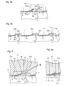
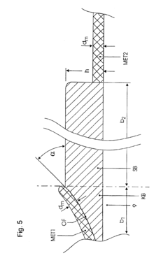
01 Silicon dioxide passivation for semiconductor devices
Silicon dioxide (SiO2) is widely used as a passivation material for P-N junction components due to its excellent electrical insulation properties and compatibility with silicon-based semiconductors. The SiO2 layer effectively reduces surface recombination velocity by neutralizing dangling bonds at the semiconductor surface, thereby improving device performance and reliability. This passivation technique is commonly applied in various semiconductor devices including solar cells, transistors, and integrated circuits to minimize leakage current and enhance overall efficiency.- Silicon oxide passivation layers for semiconductor devices: Silicon oxide (SiO2) is widely used as a passivation material for P-N junction components due to its excellent electrical insulation properties and ability to reduce surface recombination. The silicon oxide layer is typically deposited using thermal oxidation, chemical vapor deposition (CVD), or atomic layer deposition (ALD) techniques. This passivation approach effectively reduces interface states and surface leakage currents, improving the overall performance and reliability of semiconductor devices.
- Nitride-based passivation techniques: Silicon nitride (SiNx) and other nitride compounds are effective passivation materials for P-N junction components. These materials provide excellent moisture barrier properties and mechanical protection while reducing surface recombination velocities. Nitride passivation layers can be deposited using plasma-enhanced chemical vapor deposition (PECVD) or low-pressure chemical vapor deposition (LPCVD) methods. The incorporation of hydrogen during deposition can further enhance passivation quality by neutralizing dangling bonds at the semiconductor surface.
- Atomic layer deposition for ultra-thin passivation layers: Atomic Layer Deposition (ALD) enables the formation of ultra-thin, highly conformal passivation layers for P-N junction components. This technique allows precise thickness control at the atomic level and excellent step coverage, even for high-aspect-ratio structures. ALD-deposited materials such as aluminum oxide (Al2O3), hafnium oxide (HfO2), and titanium oxide (TiO2) provide effective field-effect passivation and chemical passivation simultaneously, reducing surface recombination and improving device efficiency.
- Hydrogen passivation and annealing processes: Hydrogen passivation is an effective technique for neutralizing dangling bonds at semiconductor surfaces and interfaces. This process typically involves exposing the P-N junction components to hydrogen plasma or performing annealing in a hydrogen-containing atmosphere. Post-deposition annealing treatments can significantly improve the quality of passivation layers by promoting structural relaxation, reducing defect density, and enhancing the chemical bonding between the passivation layer and the semiconductor surface.
- Advanced passivation schemes for high-efficiency devices: Modern semiconductor devices employ advanced passivation schemes that combine multiple materials and techniques to achieve superior surface passivation. These include stacked dielectric layers (such as SiO2/SiNx or Al2O3/SiNx), charged dielectric films that provide field-effect passivation, and organic/inorganic hybrid passivation layers. These sophisticated approaches are particularly important for high-efficiency photovoltaic cells, power devices, and advanced integrated circuits where minimizing surface recombination and leakage currents is critical for optimal performance.
02 Nitride-based passivation techniques
Nitride-based materials such as silicon nitride (SiNx) and aluminum nitride (AlN) are effective for surface passivation of P-N junction components. These materials provide excellent protection against moisture and ionic contamination while simultaneously offering good electrical passivation properties. The nitride layer can be deposited using various techniques including plasma-enhanced chemical vapor deposition (PECVD) and atomic layer deposition (ALD), allowing for precise thickness control and conformal coverage even on complex surface geometries. This passivation approach is particularly beneficial for power devices and optoelectronic applications.Expand Specific Solutions03 Hydrogen passivation for defect neutralization
Hydrogen passivation is an effective technique for neutralizing dangling bonds and defects at P-N junction surfaces. The process typically involves annealing the semiconductor device in a hydrogen-rich environment, allowing hydrogen atoms to diffuse into the material and bond with defect sites. This significantly reduces recombination centers at the surface and interface regions, leading to improved electrical characteristics and device performance. The technique is particularly valuable for addressing defects introduced during device fabrication processes and can be combined with other passivation methods for enhanced results.Expand Specific Solutions04 Atomic layer deposition for advanced passivation
Atomic Layer Deposition (ALD) enables the creation of ultra-thin, highly conformal passivation layers for P-N junction components with precise thickness control at the atomic scale. This technique allows for the deposition of various materials including aluminum oxide (Al2O3), hafnium oxide (HfO2), and titanium oxide (TiO2) that provide excellent surface passivation properties. The ALD process creates high-quality interfaces with minimal defects, resulting in reduced surface recombination velocities and improved device performance. This advanced passivation approach is particularly valuable for high-efficiency solar cells and next-generation semiconductor devices.Expand Specific Solutions05 Field-effect passivation techniques
Field-effect passivation utilizes fixed charges within the passivation layer to create an electric field that repels or attracts charge carriers away from the semiconductor surface, effectively reducing surface recombination. This approach often employs materials with high fixed charge densities such as aluminum oxide (Al2O3) or silicon nitride (SiNx) deposited on the semiconductor surface. The induced field effect creates either accumulation or inversion layers at the semiconductor surface, significantly reducing the concentration of one type of charge carrier and thereby minimizing recombination rates. This technique is particularly effective for high-efficiency solar cells and power devices.Expand Specific Solutions
Leading Semiconductor Manufacturers and Research Institutions
The surface passivation optimization in P-N junction components market is currently in a growth phase, with increasing demand driven by semiconductor efficiency requirements. The market size is expanding rapidly, particularly in power electronics and photovoltaics, estimated to reach several billion dollars by 2025. Technologically, established players like Infineon Technologies, Wolfspeed, and TSMC demonstrate high maturity with advanced passivation techniques, while research institutions such as Fraunhofer-Gesellschaft and South China University of Technology contribute significant innovations. Emerging companies like Naviron Technology are developing specialized solutions, while traditional semiconductor manufacturers including Sumitomo Electric and Fuji Electric are adapting their expertise to this field. The competitive landscape shows a mix of specialized component manufacturers and diversified technology conglomerates pursuing different market segments.
Wolfspeed, Inc.
Technical Solution: Wolfspeed has developed specialized surface passivation techniques specifically optimized for wide bandgap semiconductor p-n junctions, particularly for SiC and GaN devices. Their approach utilizes a proprietary post-oxidation annealing process in nitric oxide (NO) ambient to significantly reduce interface trap density at the SiC/SiO2 interface. For their SiC power devices, Wolfspeed implements a multi-step passivation process involving thermal oxidation followed by NO annealing and subsequent deposition of PECVD silicon nitride, creating a robust passivation stack that withstands high electric fields (>2 MV/cm). Their latest innovation includes phosphorus-doped SiO2 passivation layers that demonstrate a 40% reduction in interface trap density compared to conventional methods. Wolfspeed's GaN device passivation incorporates in-situ SiN deposition immediately after epitaxial growth to prevent surface contamination, resulting in significantly improved device reliability and reduced current collapse phenomena.
Strengths: Industry-leading expertise in wide bandgap semiconductor passivation; excellent high-temperature and high-field reliability; proprietary processes that enable superior device performance. Weaknesses: Higher manufacturing complexity and cost; specialized equipment requirements; limited applicability to conventional silicon-based devices.
Fraunhofer-Gesellschaft eV
Technical Solution: Fraunhofer has developed an innovative approach to surface passivation for p-n junction components using atomic layer deposition (ALD) of aluminum oxide (Al2O3) combined with hydrogen plasma treatment. Their research demonstrates that this technique achieves surface recombination velocities below 10 cm/s on both n-type and p-type silicon surfaces. The institute's proprietary process involves precise control of the negative fixed charge density (Qf > 5×10^12 cm^-2) within the Al2O3 layer, creating a strong field-effect passivation that repels minority carriers from the surface. Fraunhofer has also pioneered the development of amorphous silicon (a-Si:H) passivation layers with controlled hydrogen content, which effectively passivate dangling bonds at the crystalline silicon surface. Their latest innovation combines Al2O3 with silicon nitride (SiNx) in a stacked configuration, providing both excellent chemical passivation and effective anti-reflection properties for photovoltaic applications, resulting in conversion efficiency improvements of up to 1.2% absolute compared to conventional passivation schemes.
Strengths: Exceptional surface passivation quality with extremely low recombination velocities; excellent long-term stability; versatile application across different semiconductor materials. Weaknesses: Complex deposition processes requiring specialized equipment; higher implementation costs compared to traditional methods; challenges in scaling to very large substrate sizes.
Key Patents and Innovations in P-N Junction Passivation
Seminconductor component and method for singulating a semiconductor component having a pn junction
PatentActiveUS20220005964A1
Innovation
- A semiconductor component with a separating surface passivation layer having a surface charge density of ≥1012 cm−2 is used to prevent charge carriers from reaching the separating surface, reducing recombination effects and allowing for efficient singulation methods like TLS or LIC, which minimize surface damage and maintain electronic quality.
Termination of semiconductor components
PatentInactiveUS6956249B2
Innovation
- The use of an insulator profile with a flat base portion and a curved outward portion, produced through gray-tone lithography, which avoids peak electric field values by structuring a resist layer and etching process to create continuous, optimally curved surfaces that manage flux lines effectively, allowing for maximum blocking capacity utilization with minimal space requirements.
Environmental Impact of Passivation Materials
The environmental impact of passivation materials used in P-N junction components has become increasingly significant as semiconductor manufacturing scales globally. Traditional passivation processes often employ materials containing heavy metals, halogens, and volatile organic compounds (VOCs) that pose substantial environmental risks throughout their lifecycle. Silicon nitride (Si3N4) and silicon dioxide (SiO2), while effective for passivation, require energy-intensive chemical vapor deposition (CVD) processes that generate greenhouse gas emissions, particularly nitrogen trifluoride (NF3), which has a global warming potential 17,200 times that of CO2.
Hydrogen-based passivation techniques, though environmentally preferable to some alternatives, still require careful handling due to hydrogen's flammability and the energy requirements for its production. The manufacturing waste streams from passivation processes contain etching chemicals such as hydrofluoric acid, which demands specialized treatment facilities to prevent groundwater contamination and ecological damage.
Recent life cycle assessments of passivation materials reveal that aluminum oxide (Al2O3) deposited through atomic layer deposition (ALD) offers a significantly reduced environmental footprint compared to plasma-enhanced chemical vapor deposition (PECVD) silicon nitride. The ALD process requires approximately 40% less energy and produces fewer harmful byproducts, though it still contributes to electronic waste challenges when devices reach end-of-life.
Emerging eco-friendly alternatives include organic passivation materials derived from renewable resources. These biodegradable polymers show promising passivation properties while dramatically reducing environmental persistence. Research indicates that certain cellulose derivatives and chitosan-based compounds can provide effective surface passivation while being fully biodegradable within industrial composting conditions.
Water consumption represents another critical environmental concern in passivation processes. Traditional wet chemical passivation methods can consume up to 1,000 liters of ultra-pure water per silicon wafer, placing significant pressure on local water resources in semiconductor manufacturing regions. Dry passivation techniques are gaining attention for their potential to reduce water usage by up to 90%.
Regulatory frameworks worldwide are increasingly addressing the environmental impacts of passivation materials. The European Union's Restriction of Hazardous Substances (RoHS) and Registration, Evaluation, Authorization and Restriction of Chemicals (REACH) regulations have already restricted several passivation compounds, driving industry innovation toward greener alternatives. Similarly, China's Measures for the Administration of the Pollution Control of Electronic Information Products has accelerated the transition to environmentally benign passivation technologies in the world's largest semiconductor manufacturing market.
Integration with Advanced Semiconductor Manufacturing Processes
The integration of optimized surface passivation techniques into advanced semiconductor manufacturing processes represents a critical challenge for modern microelectronics production. Current high-volume manufacturing facilities must adapt their process flows to accommodate specialized passivation steps without compromising throughput or yield. Atomic Layer Deposition (ALD) has emerged as a preferred method for implementing advanced passivation layers, offering precise thickness control and excellent conformality even in complex 3D structures. Leading foundries have successfully integrated ALD-based passivation into their sub-10nm process nodes, demonstrating compatibility with existing manufacturing equipment.
Temperature management during passivation integration presents significant challenges, as optimal passivation often requires specific thermal budgets that must align with other process steps. Advanced facilities have developed specialized thermal cycling protocols that maintain passivation integrity while ensuring compatibility with subsequent metallization and interconnect formation. These protocols typically involve rapid thermal processing (RTP) with precisely controlled ramp rates to minimize thermal stress on passivated surfaces.
Contamination control represents another critical aspect of passivation integration. Modern clean room environments must maintain ultra-low particle counts and molecular contamination levels to ensure passivation layer quality. Enhanced filtration systems and specialized handling protocols have been implemented in leading fabs to address these requirements, with some facilities reporting defect densities below 0.01 defects/cm² for passivation-critical areas.
The economic considerations of integrating optimized passivation techniques have driven innovations in process efficiency. Multi-layer passivation schemes that combine different materials can now be applied in clustered tool configurations, reducing transfer steps and minimizing exposure to potential contaminants. This approach has reduced the cost premium for advanced passivation by approximately 30% over the past five years, making these techniques more accessible for mainstream semiconductor production.
Quality control methodologies have evolved to accommodate passivation-specific requirements. In-line monitoring techniques including ellipsometry, X-ray photoelectron spectroscopy (XPS), and electrical characterization have been adapted for high-volume manufacturing environments. These methods enable real-time feedback on passivation quality, allowing for process adjustments before significant yield impacts occur.
The roadmap for future integration focuses on developing passivation techniques compatible with emerging materials and architectures. As the industry transitions toward heterogeneous integration and advanced packaging, passivation processes must adapt to new interface challenges while maintaining compatibility with established manufacturing flows. Research consortia involving major semiconductor manufacturers are actively developing passivation solutions specifically designed for these next-generation integration scenarios.
Unlock deeper insights with PatSnap Eureka Quick Research — get a full tech report to explore trends and direct your research. Try now!
Generate Your Research Report Instantly with AI Agent
Supercharge your innovation with PatSnap Eureka AI Agent Platform!