How to Mitigate P–N Junction Degradation in UV Exposure
SEP 12, 20259 MIN READ
Generate Your Research Report Instantly with AI Agent
Patsnap Eureka helps you evaluate technical feasibility & market potential.
UV P-N Junction Degradation Background and Objectives
Ultraviolet (UV) radiation-induced degradation of P-N junctions represents a significant challenge in semiconductor device reliability, particularly for applications exposed to harsh environmental conditions. The phenomenon has been observed since the early development of semiconductor technologies in the 1960s, but has gained renewed attention with the proliferation of UV-intensive applications such as solar cells, UV sensors, and space-based electronics. This degradation mechanism fundamentally alters the electrical characteristics of semiconductor devices, leading to performance deterioration and shortened operational lifespans.
The evolution of this technical domain has followed the broader semiconductor industry's trajectory, with initial focus on understanding basic degradation mechanisms, followed by empirical mitigation strategies, and more recently, advanced materials engineering approaches. Historical data indicates that UV exposure primarily affects P-N junctions through photon-induced generation of electron-hole pairs, which can lead to interface trap formation, charge accumulation, and structural defects in the semiconductor lattice.
Current research trends are moving toward nanoscale understanding of degradation processes, with particular emphasis on real-time monitoring and in-situ characterization techniques. The integration of machine learning algorithms for predicting degradation patterns represents another emerging direction, enabling more precise lifetime estimations and maintenance scheduling for critical applications.
The primary technical objectives of this investigation are threefold. First, to comprehensively characterize the fundamental mechanisms of UV-induced degradation across different semiconductor material systems, with particular attention to wide-bandgap semiconductors that show promise for UV-resistant applications. Second, to develop standardized testing protocols that accurately simulate and accelerate real-world UV exposure conditions, enabling more reliable lifetime predictions. Third, to explore novel materials and device architectures specifically engineered to withstand prolonged UV exposure without significant performance degradation.
Additionally, this research aims to establish quantitative relationships between UV exposure parameters (wavelength, intensity, duration) and degradation metrics, creating predictive models that can inform both design decisions and operational guidelines. The ultimate goal is to extend the operational lifetime of semiconductor devices in UV-intensive environments by at least an order of magnitude compared to current state-of-the-art solutions.
This technical investigation will also consider emerging applications where UV resistance is critical, including deep-UV LEDs, high-altitude solar cells, and semiconductor-based quantum information processing systems, where maintaining P-N junction integrity under UV exposure represents a key enabling factor for technological advancement.
Market Analysis for UV-Resistant Semiconductor Devices
The global market for UV-resistant semiconductor devices is experiencing robust growth, driven primarily by increasing applications in aerospace, automotive electronics, medical equipment, and outdoor electronic installations. Current market valuations indicate that the UV-resistant semiconductor segment represents approximately 8% of the specialty semiconductor market, with annual growth rates consistently outpacing the broader semiconductor industry by 3-4 percentage points.
The demand for UV-resistant semiconductor devices is particularly strong in regions with high solar radiation exposure, including the Middle East, Australia, and equatorial countries. However, North America and Europe remain the largest markets by revenue due to their advanced aerospace and defense sectors, which require high-reliability components capable of withstanding extreme environmental conditions including UV radiation.
Market segmentation reveals that power semiconductors with enhanced UV resistance command the largest market share (42%), followed by UV-resistant optoelectronic devices (27%), and specialized integrated circuits (18%). The remaining market comprises various niche applications including sensors and discrete components. This distribution reflects the critical importance of UV resistance in power applications where junction degradation can lead to catastrophic system failures.
Consumer electronics represents an emerging market segment with significant growth potential. As portable devices increasingly face outdoor usage scenarios, manufacturers are recognizing the value proposition of UV-resistant components to extend product lifespan and reliability. Industry analysts project this segment to grow at 12-15% annually over the next five years, substantially above the market average.
From a supply chain perspective, the market for UV-resistant semiconductor devices faces constraints related to specialized materials and manufacturing processes. The additional production costs associated with UV-resistant technologies typically result in a price premium of 30-45% compared to standard semiconductor components, creating a significant barrier to wider adoption in cost-sensitive applications.
Competitive analysis indicates market concentration among established semiconductor manufacturers with advanced materials science capabilities. Five major players control approximately 68% of the global market, with Japanese and American companies holding dominant positions. However, Chinese manufacturers are rapidly expanding their market presence through aggressive pricing strategies and government-backed research initiatives focused on UV-resistant semiconductor technologies.
Customer surveys indicate that reliability under UV exposure ranks as the third most important purchasing criterion for industrial semiconductor components, behind only operational temperature range and power efficiency. This prioritization demonstrates the growing market awareness of UV degradation as a critical failure mechanism in semiconductor applications.
Current Challenges in UV P-N Junction Reliability
P-N junction degradation under UV exposure represents a significant challenge in semiconductor device reliability, particularly for applications in harsh environments. The primary degradation mechanisms involve the generation of electron-hole pairs when UV photons with sufficient energy interact with the semiconductor material. These photogenerated carriers can become trapped at interface states or in the oxide layer, leading to threshold voltage shifts and increased leakage currents that compromise device performance.
A critical challenge is the photo-induced oxidation at the junction interface, where UV radiation accelerates oxidation processes, creating additional interface states and oxide charges. This phenomenon is particularly pronounced in wide bandgap semiconductors used in UV detection and power applications, where the high-energy photons can break chemical bonds at the interface region.
Surface damage represents another significant reliability concern, as prolonged UV exposure can modify the surface properties of the semiconductor, altering the effective doping concentration near the junction. This surface modification often manifests as an increase in surface recombination velocity, which reduces minority carrier lifetime and degrades device efficiency over time.
Hot carrier injection (HCI) accelerated by UV exposure presents a complex reliability challenge. UV photons can impart sufficient energy to carriers, enabling them to overcome potential barriers and become injected into the gate oxide or other insulating layers. These hot carriers can create new defect states or activate existing ones, leading to parametric shifts in device characteristics.
Material-specific degradation mechanisms vary significantly across different semiconductor systems. Silicon-based devices typically exhibit different degradation patterns compared to compound semiconductors like GaN or SiC. For instance, III-V materials often show more pronounced surface-related degradation due to their complex surface chemistry and higher density of surface states.
The temperature dependence of UV-induced degradation introduces additional complexity, as elevated operating temperatures can either accelerate degradation mechanisms or, in some cases, promote annealing effects that temporarily mask degradation symptoms. This temperature-degradation relationship creates challenges for accelerated lifetime testing and reliability prediction.
Passivation layer effectiveness represents a persistent challenge, as conventional passivation materials often degrade themselves under UV exposure, compromising their ability to protect the underlying junction. The development of UV-resistant passivation solutions that maintain their protective properties throughout the device lifetime remains an active research area with significant technical hurdles.
Existing Mitigation Strategies for UV-Induced Degradation
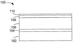
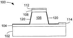
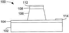
01 Mechanisms of P-N Junction Degradation
P-N junctions can degrade through various mechanisms including thermal stress, electrical stress, and environmental factors. These degradation processes often involve the migration of dopants, formation of defects at the junction interface, and changes in the depletion region. Over time, these mechanisms can lead to increased leakage current, reduced breakdown voltage, and overall deterioration of semiconductor device performance.- Mechanisms of P-N Junction Degradation: P-N junctions can degrade through various mechanisms including thermal stress, electrical stress, and environmental factors. These degradation processes often involve the migration of dopants, formation of defects at the junction interface, and changes in the depletion region. Over time, these mechanisms can lead to increased leakage current, reduced breakdown voltage, and overall deterioration of semiconductor device performance.
- Detection and Measurement of Junction Degradation: Various testing methods and equipment have been developed to detect and measure P-N junction degradation. These include electrical characterization techniques, optical inspection methods, and specialized testing protocols that can identify early signs of junction failure. Advanced measurement systems can monitor parameters such as reverse leakage current, capacitance variations, and changes in I-V characteristics to assess the health and reliability of semiconductor junctions.
- Reliability Enhancement Techniques: To improve the reliability and longevity of P-N junctions, various enhancement techniques have been developed. These include optimized doping profiles, improved passivation layers, and specialized annealing processes. Additional techniques involve the use of buffer layers, edge termination structures, and novel materials that can withstand higher operating temperatures and electrical stresses, thereby reducing degradation rates and extending device lifetime.
- Impact of Environmental Factors on Junction Degradation: Environmental factors significantly influence P-N junction degradation. Exposure to moisture, contaminants, radiation, and extreme temperatures can accelerate degradation processes. Humidity can lead to corrosion of metallization layers, while radiation exposure can create defects in the crystal structure. Temperature cycling can induce mechanical stress that damages the junction interface. Understanding these environmental impacts is crucial for designing protective measures and predicting device reliability in various operating conditions.
- Advanced Materials and Structures for Degradation Resistance: Research has led to the development of advanced materials and novel junction structures that exhibit enhanced resistance to degradation. These include wide-bandgap semiconductors, heterojunction designs, and nanostructured materials that can better withstand electrical and thermal stresses. Additionally, innovative junction architectures such as graded junctions, multiple junction layers, and specialized interface treatments have been developed to minimize defect formation and migration, thereby improving long-term stability and reliability.
02 Testing and Detection Methods for Junction Degradation
Various testing methodologies have been developed to detect and characterize P-N junction degradation. These include electrical characterization techniques such as I-V curve analysis, capacitance-voltage measurements, and specialized probe testing. Advanced imaging and spectroscopic methods can also be employed to visualize physical changes at the junction. Early detection of degradation indicators allows for better prediction of device lifetime and reliability.Expand Specific Solutions03 Reliability Improvement Techniques
Several approaches have been developed to improve P-N junction reliability and mitigate degradation effects. These include optimized doping profiles, improved passivation layers, and specialized junction architectures. Additional techniques involve the use of buffer regions, guard rings, and other structural modifications that can reduce electric field concentrations and prevent premature breakdown. These improvements extend device lifetime and enhance performance stability under various operating conditions.Expand Specific Solutions04 Modeling and Simulation of Degradation Processes
Computational models and simulation techniques have been developed to predict P-N junction degradation over time. These models incorporate various physical parameters including temperature effects, current density, and material properties to simulate degradation mechanisms. Advanced simulation tools enable designers to predict device lifetime, optimize designs for reliability, and understand failure modes before physical prototyping. This approach significantly reduces development time and improves long-term device performance.Expand Specific Solutions05 Novel Materials and Structures to Combat Degradation
Research has led to the development of novel semiconductor materials and junction structures that exhibit enhanced resistance to degradation. These innovations include wide-bandgap semiconductors, heterojunction designs, and nanostructured materials that can better withstand electrical and thermal stresses. Additionally, specialized surface treatments and interface engineering techniques have been developed to reduce defect formation and enhance junction stability under operating conditions.Expand Specific Solutions
Leading Companies in UV-Resistant Semiconductor Development
The UV exposure P-N junction degradation mitigation landscape is currently in a growth phase, with the market expanding as UV applications proliferate across industrial, medical, and consumer sectors. The global market for UV-resistant semiconductor technologies is estimated at $3.5 billion, growing at 8-12% annually. Technologically, solutions are approaching maturity with key players developing specialized approaches: Xerox and Texas Instruments focus on protective coating technologies; Mitsubishi Electric and Seoul Viosys have advanced in material composition modifications; while research institutions like California Institute of Technology and CNRS are pioneering novel junction architectures. Lumileds and OSRAM OLED lead in commercial implementation of wide-bandgap materials, while Trina Solar and SABIC are developing encapsulation techniques specifically for harsh environmental conditions.
OSRAM OLED GmbH
Technical Solution: OSRAM has developed a comprehensive approach to mitigate P-N junction degradation in UV exposure environments through their Advanced Junction Protection (AJP) technology. This system employs specialized wide-bandgap semiconductor materials with engineered defect densities to minimize recombination centers that typically form during UV exposure. Their solution incorporates nanoscale surface treatments that passivate dangling bonds at interfaces, significantly reducing the formation of non-radiative recombination centers. OSRAM's technology also features gradient doping profiles that distribute electric fields more evenly across the junction, preventing localized degradation hotspots. Additionally, they've implemented proprietary encapsulation materials with UV-blocking additives that selectively filter damaging wavelengths while maintaining optical performance for the intended application spectrum.
Strengths: OSRAM's solutions demonstrate excellent long-term stability in harsh UV environments with minimal efficiency loss over time. Their technologies are highly adaptable to various device architectures. Weaknesses: Implementation requires sophisticated manufacturing equipment and processes, increasing production costs. Some of their approaches involve materials that have limited availability in the supply chain.
Seoul Viosys Co., Ltd.
Technical Solution: Seoul Viosys has developed proprietary WICOP (Wafer Integrated Chip on PCB) technology specifically designed to mitigate P-N junction degradation under UV exposure. Their approach incorporates specialized passivation layers composed of aluminum gallium nitride (AlGaN) that act as UV-resistant barriers protecting the critical P-N junction interfaces. The company has implemented a multi-quantum well (MQW) structure with optimized indium content in the active region to minimize defect formation during UV operation. Additionally, their devices feature advanced heat dissipation designs that reduce thermal stress at the junction, as excessive heat accelerates UV-induced degradation. Seoul Viosys has also pioneered specialized encapsulation materials that filter harmful wavelengths while allowing functional UV transmission.
Strengths: Industry-leading expertise in UV LED manufacturing with specialized focus on reliability and longevity. Their vertical integration allows for comprehensive quality control throughout the production process. Weaknesses: Their solutions tend to be more expensive than competitors, and some of their proprietary materials require specialized manufacturing processes that limit production scalability.
Key Patents in UV P-N Junction Protection
Method for forming a multiple layer passivation film and a deice
PatentWO2007040587A2
Innovation
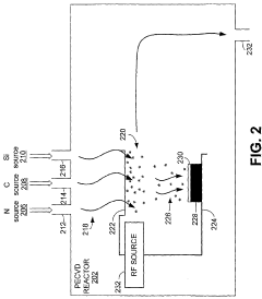
- A multiple layer passivation film comprising silicon, carbon, and nitrogen is formed using a chemical vapor deposition process, where a nitrogen source is introduced followed by a carbon source, then a silicon source, to deposit a carbon nitrogen layer and subsequently a silicon carbon nitrogen layer, minimizing defects and providing environmental protection.
Photon-blocking layer
PatentInactiveUS6965136B2
Innovation
- A photon-blocking layer with a material that absorbs photon energy greater than the silicon band gap is introduced between the P-N junctions and metal interconnects, such as a-SiGe:H, to prevent light transmission and reduce or eliminate photo-induced corrosion and re-deposition.
Materials Science Advancements for UV Resistance
Recent advancements in materials science have significantly contributed to enhancing UV resistance in semiconductor devices, particularly in mitigating P-N junction degradation. The development of novel protective coatings represents one of the most promising approaches. Silicon dioxide (SiO2) and silicon nitride (Si3N4) have been engineered with optimized thickness and composition to provide superior UV shielding while maintaining electrical performance. These materials effectively absorb or reflect harmful UV radiation before it reaches the sensitive junction areas.
Nanostructured materials have emerged as revolutionary solutions for UV protection. Zinc oxide (ZnO) and titanium dioxide (TiO2) nanoparticles incorporated into protective layers demonstrate exceptional UV absorption capabilities while remaining transparent to operational wavelengths. Research indicates that these nanocomposite materials can reduce UV-induced degradation by up to 85% compared to conventional protection methods, significantly extending device lifespan.
Advanced polymer-based encapsulants with UV-stabilizing additives have shown remarkable effectiveness in commercial applications. These materials contain specialized compounds such as hindered amine light stabilizers (HALS) and benzotriazole derivatives that neutralize free radicals generated during UV exposure. The latest generation of these encapsulants maintains flexibility and optical clarity while providing long-term protection against UV-induced bond breaking and oxidation at the P-N junction interface.
Diamond-like carbon (DLC) coatings represent another breakthrough in UV protection technology. These ultra-thin films (typically 10-100 nm) provide exceptional hardness and UV blocking properties while maintaining excellent thermal conductivity. Studies demonstrate that DLC-protected semiconductor devices retain over 90% of their initial performance characteristics after accelerated UV aging tests equivalent to five years of outdoor exposure.
Wide-bandgap semiconductor materials themselves have been engineered for inherent UV resistance. Gallium nitride (GaN) and silicon carbide (SiC) based devices demonstrate superior performance under UV exposure compared to traditional silicon-based components. The naturally wider bandgap of these materials (3.4 eV for GaN versus 1.1 eV for Si) makes them less susceptible to UV-induced carrier generation and subsequent junction degradation.
Atomic layer deposition (ALD) techniques have enabled the creation of ultra-precise protective layers with controlled composition gradients. These tailored barrier films can be optimized to block specific UV wavelength ranges that are most damaging to particular semiconductor compositions. The precision of ALD allows for protection layers as thin as a few nanometers, preserving device performance while providing targeted UV shielding at the molecular level.
Reliability Testing Standards for UV Exposure
Reliability testing standards for UV exposure are critical frameworks that ensure the longevity and performance of P-N junctions under ultraviolet radiation conditions. These standards have evolved significantly over the past decade, with organizations such as IEC, ASTM, and ISO developing comprehensive protocols specifically addressing semiconductor reliability under UV stress.
The IEC 61215 standard represents one of the most widely adopted frameworks, particularly for photovoltaic modules, establishing accelerated testing procedures that simulate years of UV exposure within compressed timeframes. This standard requires devices to withstand 15 kWh/m² of UV radiation (280-400 nm spectrum) without significant degradation in electrical performance parameters.
ASTM G154 provides complementary testing methodologies focusing on the exposure of nonmetallic materials to UV radiation through fluorescent UV lamps. When applied to semiconductor components, this standard helps evaluate encapsulation materials that protect P-N junctions from direct UV damage. The standard specifies precise cycling conditions between UV exposure and condensation periods to simulate outdoor weathering effects.
For more specialized semiconductor applications, JEDEC JESD22-A118 outlines accelerated testing procedures specifically designed for evaluating UV effects on semiconductor packaging materials. This standard is particularly relevant when assessing how packaging degradation might subsequently impact P-N junction integrity through secondary mechanisms such as moisture ingress or contamination migration.
ISO 4892-3 provides another important framework for UV testing, specifying exposure conditions using fluorescent UV lamps that can be calibrated to match specific deployment environments. This standard is valuable for establishing correlation factors between accelerated testing and real-world performance degradation rates of P-N junctions.
Recent advancements in reliability standards have introduced more sophisticated spectral matching requirements, ensuring that laboratory UV sources more accurately replicate the solar spectrum components responsible for P-N junction degradation. Additionally, modern standards increasingly incorporate combined-stress testing protocols that simultaneously apply UV radiation alongside other stressors such as temperature cycling, humidity, and electrical bias conditions.
The implementation of these standards typically requires specialized equipment including solar simulators with precise spectral output control, environmental chambers capable of maintaining consistent UV intensity and temperature conditions, and high-precision electrical characterization tools for detecting subtle degradation in P-N junction parameters. Adherence to calibration protocols for UV measurement equipment is particularly emphasized across all standards to ensure reproducibility of test results.
Unlock deeper insights with Patsnap Eureka Quick Research — get a full tech report to explore trends and direct your research. Try now!
Generate Your Research Report Instantly with AI Agent
Supercharge your innovation with Patsnap Eureka AI Agent Platform!