Optimize Electric Field Distribution in P–N Junction Designs
SEP 12, 20259 MIN READ
Generate Your Research Report Instantly with AI Agent
Patsnap Eureka helps you evaluate technical feasibility & market potential.
P-N Junction Electric Field Optimization Background and Objectives
The P-N junction stands as one of the most fundamental structures in semiconductor physics and electronic devices, serving as the building block for numerous applications including diodes, transistors, solar cells, and integrated circuits. Since its discovery in the early 20th century, optimizing the electric field distribution within P-N junctions has been a critical focus for enhancing device performance, efficiency, and reliability.
The evolution of P-N junction technology has progressed through several significant phases. Initially, the focus was on basic understanding of carrier transport mechanisms and junction formation. This was followed by advancements in fabrication techniques that allowed for more precise control of doping profiles. Recent decades have witnessed sophisticated approaches to junction engineering, including graded junctions, heterojunctions, and nanoscale structures, all aimed at manipulating electric field distribution for specific applications.
Current technological trends indicate a growing emphasis on achieving finer control over electric field profiles to address emerging challenges in power electronics, high-frequency applications, and energy conversion devices. The miniaturization of semiconductor devices continues to push the boundaries of conventional P-N junction designs, necessitating novel approaches to electric field management at nanoscale dimensions.
The primary technical objectives for P-N junction electric field optimization encompass several key areas. First, reducing peak electric field concentrations to enhance breakdown voltage characteristics while maintaining low on-state resistance—a critical parameter for power electronic applications. Second, engineering field distributions to accelerate carrier transport for high-frequency operation. Third, optimizing field profiles to minimize recombination losses in photovoltaic and optoelectronic devices.
Additionally, there is increasing interest in developing junction designs that can withstand extreme operating conditions, including high temperatures, radiation environments, and high-power densities. These requirements are particularly relevant for applications in aerospace, automotive, and industrial sectors where reliability under harsh conditions is paramount.
The intersection of computational modeling techniques with experimental validation has emerged as a powerful methodology for advancing P-N junction optimization. Simulation tools now enable prediction of electric field behavior with unprecedented accuracy, allowing for iterative design improvements before physical fabrication. This approach has significantly accelerated the development cycle and expanded the design space for novel junction architectures.
As we look toward future developments, the integration of new materials, including wide-bandgap semiconductors and two-dimensional materials, presents both challenges and opportunities for electric field optimization in next-generation electronic devices.
Market Applications and Demand Analysis for Optimized P-N Junctions
The global market for optimized P-N junctions demonstrates robust growth driven by increasing demand across multiple sectors. Power electronics represents the largest application segment, with the market expected to reach $25 billion by 2027, growing at a CAGR of 8.3%. This growth is primarily fueled by the rapid expansion of electric vehicles, renewable energy systems, and industrial automation requiring high-efficiency power conversion components.
Consumer electronics constitutes another significant market segment, where optimized P-N junctions enable more efficient and compact semiconductor devices. The smartphone industry alone consumes over 1.5 billion semiconductor units annually, with manufacturers constantly seeking components that reduce power consumption while maintaining or improving performance characteristics.
The renewable energy sector presents particularly compelling market opportunities. Solar photovoltaic installations continue to accelerate globally, with annual capacity additions exceeding 200 GW. Enhanced P-N junction designs directly impact solar cell efficiency, with each percentage point improvement in conversion efficiency potentially generating billions in additional market value.
Medical electronics represents an emerging high-value application area, with demand for miniaturized, low-power devices growing at approximately 12% annually. Optimized P-N junctions enable longer battery life and improved performance in implantable devices, patient monitoring systems, and diagnostic equipment.
Regional analysis reveals Asia-Pacific as the dominant manufacturing hub, accounting for over 60% of global production capacity for semiconductor devices utilizing advanced P-N junction designs. However, recent geopolitical tensions have accelerated efforts to diversify supply chains, with significant investments in new manufacturing facilities across North America and Europe.
Market research indicates that devices incorporating optimized electric field distribution in P-N junctions command premium pricing, with margins typically 15-25% higher than conventional alternatives. This price premium reflects the tangible performance benefits, including reduced power consumption, improved thermal management, and enhanced reliability under variable operating conditions.
Customer demand increasingly emphasizes sustainability metrics alongside traditional performance parameters. Semiconductor manufacturers report growing interest in components that enable end products to meet stringent energy efficiency regulations and sustainability certifications, creating additional market pull for optimized P-N junction technologies.
Current Challenges in Electric Field Distribution Technology
Despite significant advancements in semiconductor technology, optimizing electric field distribution in P-N junctions remains a persistent challenge for device engineers. Current P-N junction designs face several critical limitations that impede performance optimization and reliability. The non-uniform electric field distribution at junction edges creates localized high-field regions that trigger premature breakdown, significantly limiting device operating voltage and overall efficiency.
Temperature sensitivity presents another major obstacle, as electric field profiles change substantially with operating temperature fluctuations. This thermal dependence creates reliability issues in applications requiring stable performance across wide temperature ranges, particularly affecting power electronics and automotive semiconductors where thermal cycling is common.
Surface termination techniques, while improved, still struggle to effectively manage field crowding at device peripheries. Conventional techniques like floating field rings and field plates add manufacturing complexity and consume valuable die area without fully resolving edge termination challenges, especially in high-voltage applications exceeding 1200V.
The miniaturization trend in semiconductor devices has intensified these challenges, as reduced dimensions lead to higher field concentrations in smaller volumes. This scaling issue is particularly problematic in modern integrated circuits where device density continues to increase while maintaining reliability requirements. The resulting high field gradients accelerate various degradation mechanisms including hot carrier injection and time-dependent dielectric breakdown.
Material interface management presents additional complications, especially in heterojunction designs where lattice mismatches and band discontinuities create complex field distributions. These interface effects are difficult to model accurately and often lead to unexpected device behavior that deviates from theoretical predictions.
Simulation limitations further compound these challenges. Current TCAD tools struggle to simultaneously model all relevant physical phenomena affecting electric field distribution, particularly when quantum effects become significant in nanoscale devices. The computational resources required for accurate multi-physics simulations often force engineers to make simplifying assumptions that reduce prediction accuracy.
Manufacturing variability introduces another layer of complexity, as process variations in doping profiles, junction depths, and interface qualities create device-to-device inconsistencies in field distribution. This variability makes it difficult to achieve uniform performance across production batches and complicates statistical design approaches needed for high-yield manufacturing.
These challenges collectively highlight the need for innovative approaches to electric field engineering in P-N junctions, driving research toward novel materials, junction architectures, and simulation methodologies that can overcome current limitations.
Contemporary Methods for Electric Field Distribution Optimization
01 Electric field distribution modeling in P-N junctions
Various methods and models are used to analyze and predict the electric field distribution in P-N junctions. These include computational simulations, mathematical modeling, and analytical approaches that help understand how the electric field varies across the depletion region. These models account for factors such as doping concentration, junction geometry, and applied voltage to accurately represent the electric field behavior in semiconductor devices.- Electric field distribution modeling in P-N junctions: Various methods and models are used to analyze and predict the electric field distribution in P-N junctions. These include computational simulations, mathematical modeling, and analytical approaches that help understand how the electric field varies across the depletion region. Such models are crucial for designing semiconductor devices with optimal performance characteristics and for predicting device behavior under different operating conditions.
- Electric field control techniques in semiconductor devices: Techniques for controlling and manipulating the electric field distribution in P-N junctions involve structural modifications, doping profile adjustments, and the introduction of additional layers or materials. These approaches allow for tailored electric field profiles that can enhance device performance, reduce breakdown phenomena, and improve reliability in various semiconductor applications.
- Measurement and characterization of P-N junction electric fields: Methods and apparatus for measuring and characterizing the electric field distribution in P-N junctions include specialized probing techniques, optical measurements, and electrical testing procedures. These measurement approaches provide critical data for validating theoretical models, quality control in manufacturing, and understanding the actual behavior of fabricated devices under real operating conditions.
- Electric field effects on P-N junction performance: The distribution of electric fields in P-N junctions significantly impacts device performance parameters such as breakdown voltage, leakage current, switching speed, and power efficiency. Understanding these relationships helps in designing semiconductor devices with optimized characteristics for specific applications, from power electronics to integrated circuits and optoelectronic devices.
- Novel structures for electric field engineering: Innovative semiconductor structures and junction designs are developed to achieve specific electric field distributions. These include gradient doping profiles, junction termination extensions, field plates, and heterojunction structures. Such novel approaches enable enhanced performance in high-power applications, improved efficiency in energy conversion devices, and better reliability in extreme operating environments.
02 Electric field manipulation techniques in semiconductor devices
Techniques for manipulating and controlling the electric field distribution in P-N junctions to achieve desired device characteristics. These include structural modifications, doping profile engineering, and the introduction of additional layers or materials to shape the electric field. Such manipulation allows for optimization of device performance, reduction of breakdown effects, and enhancement of specific electrical properties.Expand Specific Solutions03 Measurement and characterization of P-N junction electric fields
Methods and apparatus for measuring and characterizing the electric field distribution in P-N junctions. These include specialized probing techniques, optical measurements, and electrical testing methodologies that provide insights into the actual field distribution within fabricated devices. Such measurements are crucial for validating theoretical models and ensuring proper device operation.Expand Specific Solutions04 Electric field effects on P-N junction performance
Analysis of how electric field distribution affects the performance and reliability of semiconductor devices with P-N junctions. This includes studies on breakdown mechanisms, leakage currents, carrier transport, and device efficiency as influenced by the electric field profile. Understanding these effects is essential for designing robust semiconductor devices with optimal performance characteristics.Expand Specific Solutions05 Novel P-N junction structures for electric field optimization
Innovative P-N junction designs and structures specifically developed to achieve optimized electric field distributions. These include gradient doping profiles, heterojunctions, multiple junction configurations, and the incorporation of buffer layers or field plates. Such novel structures enable enhanced device performance, higher breakdown voltages, and improved reliability in various semiconductor applications.Expand Specific Solutions
Leading Companies and Research Institutions in Semiconductor Technology
The electric field distribution optimization in P-N junction designs is currently in a mature development stage, with a global market estimated at $25-30 billion annually. The competitive landscape features established semiconductor manufacturers like Taiwan Semiconductor Manufacturing Co., Infineon Technologies, and Mitsubishi Electric driving commercial applications, while research institutions such as University of Electronic Science & Technology of China and Fraunhofer-Gesellschaft lead academic innovation. Technical maturity varies across applications, with power electronics showing high maturity through companies like MaxPower Semiconductor and Fuji Electric, while emerging applications in optoelectronics (OSI Optoelectronics) and renewable energy (Innovalight) remain in development phases. The field is characterized by cross-sector collaboration between academic institutions and industry players to overcome remaining technical challenges in junction efficiency and reliability.
Toshiba Corp.
Technical Solution: Toshiba has developed advanced P-N junction electric field optimization techniques through their DTMOS (Deep Trench MOSFET) and LGBT (Lateral Gate Bipolar Transistor) technologies. Their approach involves creating three-dimensional junction structures with precisely controlled depth profiles to distribute electric fields more uniformly. Toshiba implements a proprietary Super Junction architecture that alternates thin vertical P and N pillars to spread the depletion region throughout the device volume rather than concentrating at a planar interface. For edge termination, they've developed a graduated field ring system where multiple concentric rings with optimized spacing and doping create a stepped field reduction toward device periphery. Their recent innovations include semi-insulating buffer layers that help reshape the electric field distribution in compound semiconductor devices. Toshiba also employs advanced passivation techniques using specialized dielectric materials with engineered permittivity to further modify field distributions at critical interfaces[2][8]. Their manufacturing process includes precision epitaxial growth with in-situ doping to create ultra-smooth doping transitions that eliminate abrupt field changes.
Strengths: Strong expertise in both silicon and compound semiconductor junction optimization; established manufacturing processes for complex 3D structures; excellent integration of materials science into junction design. Weaknesses: Some techniques require extremely precise process control that may impact yield; optimization approaches often involve trade-offs between breakdown voltage and on-resistance; solutions may be more complex to implement than conventional approaches.
Mitsubishi Electric Corp.
Technical Solution: Mitsubishi Electric has developed sophisticated P-N junction electric field optimization techniques primarily for their high-voltage power semiconductor devices. Their approach centers on a proprietary guard ring termination structure that effectively distributes electric field concentrations at junction edges. Mitsubishi implements a multi-step field plate design that extends over the junction area with precisely calculated overlaps to reshape the equipotential lines and prevent field crowding. For their IGBT products, they've pioneered a unique carrier lifetime control technology using helium irradiation that allows for precise manipulation of the electric field profile throughout the drift region. Their recent advancements include three-dimensional trench gate structures with optimized corner profiles to eliminate field enhancement points. Mitsubishi also employs advanced numerical simulation techniques that incorporate both electrostatic and carrier transport models to predict field distributions under various operating conditions[3][7]. Their manufacturing process includes specialized annealing steps that reduce interface charges which can distort electric field uniformity at critical junction boundaries.
Strengths: Extensive experience in high-voltage device design where field management is critical; proven manufacturing processes for complex junction structures; strong integration between simulation and fabrication. Weaknesses: Solutions primarily focused on power applications rather than signal processing; some techniques require specialized processing equipment not widely available; optimization approaches may trade off switching speed for field uniformity.
Critical Patents and Research in P-N Junction Engineering
Semiconductor substrate comprising doped regions forming a p-n junction
PatentActiveEP2551896A1
Innovation
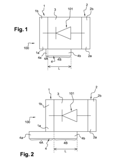
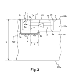
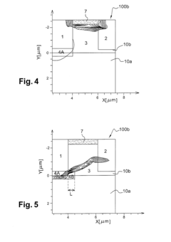
- A semiconductor substrate design featuring a P-N junction with a fourth doped zone positioned between the first and second doped zones, where the fourth zone has a lower doping concentration than the first and second zones, allowing for higher voltage handling while preventing electrical breakdown by optimizing its dimensions using techniques like TCAD modeling.
Ultra-Thin Super Junction IGBT Device and Manufacturing Method Thereof
PatentActiveUS20230155014A1
Innovation
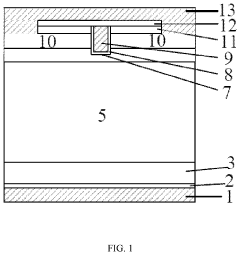
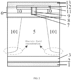
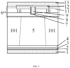
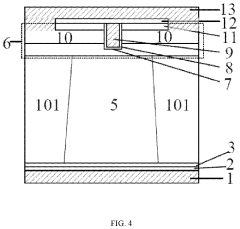
- An ultra-thin super junction IGBT is developed with a metalized collector, P-type collector region, N-type FS layer, N-type FS isolating layer, and epitaxial layers, utilizing deep trench etching and reactive ion etching processes to form a floating P column and reduce the thickness, along with implantation of N-type and P-type impurities to alleviate electric field concentration and enhance conductivity.
Materials Science Advancements for Enhanced P-N Junction Performance
Recent advancements in materials science have significantly contributed to enhancing P-N junction performance, particularly in optimizing electric field distribution. Traditional silicon-based semiconductors are increasingly being supplemented or replaced by novel materials that offer superior electrical properties and greater design flexibility.
Compound semiconductors such as gallium arsenide (GaAs), gallium nitride (GaN), and silicon carbide (SiC) have emerged as promising alternatives due to their wider bandgaps and higher electron mobility. These properties allow for more efficient electric field management across the junction interface, resulting in reduced leakage currents and improved thermal stability under high-voltage operations.
Nanomaterials represent another frontier in P-N junction optimization. Two-dimensional materials like graphene and transition metal dichalcogenides (TMDs) exhibit unique quantum confinement effects that can be leveraged to create atomically thin junctions with precisely controlled electric field profiles. These materials enable the development of ultra-compact devices with reduced parasitic capacitance and enhanced switching speeds.
The incorporation of heterojunction structures, where dissimilar semiconductor materials are combined, has proven effective in tailoring electric field distributions. By engineering the band alignment between materials with different electron affinities and bandgaps, researchers can create built-in electric fields that enhance carrier separation and reduce recombination losses. This approach has been particularly valuable in photovoltaic applications.
Surface modification techniques have also advanced significantly, allowing for precise control over interface states that influence electric field distribution. Atomic layer deposition (ALD) and molecular beam epitaxy (MBE) enable the creation of atomically precise interfaces with minimal defect densities, reducing charge trapping and improving carrier transport across the junction.
Strain engineering represents another promising direction, where mechanical stress is deliberately introduced to modify the band structure and carrier mobility of semiconductor materials. By applying tensile or compressive strain to specific regions of the P-N junction, the electric field distribution can be optimized to enhance device performance in targeted applications.
The integration of dielectric engineering approaches has further expanded design possibilities. High-k dielectrics and engineered insulator layers can be strategically positioned to reshape electric field contours, mitigating edge effects and preventing premature breakdown in high-power devices. These advances are particularly important for wide-bandgap semiconductor devices operating at elevated voltages.
Simulation and Modeling Tools for Electric Field Optimization
The evolution of simulation and modeling tools for electric field optimization in P-N junctions has significantly accelerated semiconductor device development. Traditional analytical approaches have given way to sophisticated computational methods that provide unprecedented accuracy in predicting electric field distributions across junction interfaces.
TCAD (Technology Computer-Aided Design) platforms represent the cornerstone of modern electric field simulation, with Synopsys Sentaurus and Silvaco Atlas leading the industry. These comprehensive suites offer multiphysics capabilities that integrate electrostatic calculations with thermal effects, carrier transport mechanisms, and quantum phenomena. Recent versions have incorporated machine learning algorithms to accelerate convergence in complex junction geometries.
Finite Element Method (FEM) and Finite Difference Time Domain (FDTD) techniques form the mathematical foundation of these tools, enabling discretization of the semiconductor structure into meshes of varying density. Advanced adaptive meshing algorithms automatically refine resolution in regions of high field gradients, particularly critical at abrupt junction interfaces where field crowding occurs.
Monte Carlo simulation methods have emerged as powerful complements to deterministic approaches, especially for modeling statistical variations in dopant distributions that significantly impact local electric field profiles. These probabilistic techniques provide valuable insights into device reliability by identifying potential breakdown points under various operating conditions.
Open-source alternatives have gained traction in research environments, with tools like DEVSIM and Cogenda GENIUS offering comparable capabilities to commercial packages. Python-based frameworks leveraging libraries such as FEniCS and NGSolve have democratized access to advanced simulation capabilities, fostering innovation in junction design optimization.
Quantum-corrected models have become increasingly important as device dimensions approach nanometer scales. Density Functional Theory (DFT) and Non-Equilibrium Green's Function (NEGF) methods now supplement classical drift-diffusion models to accurately capture quantum confinement effects on electric field distributions in ultra-thin junction regions.
Cloud-based simulation platforms represent the latest evolution, enabling parameter sweeps and optimization routines that were previously computationally prohibitive. These services leverage parallel processing architectures to explore vast design spaces, identifying optimal junction profiles that minimize field crowding while maintaining desired electrical characteristics.
The integration of AI-driven optimization algorithms with physics-based simulators marks the frontier of electric field modeling tools, promising automated discovery of novel junction geometries that outperform conventional designs in terms of breakdown voltage, switching speed, and power efficiency.
Unlock deeper insights with Patsnap Eureka Quick Research — get a full tech report to explore trends and direct your research. Try now!
Generate Your Research Report Instantly with AI Agent
Supercharge your innovation with Patsnap Eureka AI Agent Platform!
