How to Enhance P–N Junction Efficiency for Solar Cells
SEP 4, 20259 MIN READ
Generate Your Research Report Instantly with AI Agent
Patsnap Eureka helps you evaluate technical feasibility & market potential.
Solar Cell P-N Junction Background and Objectives
The photovoltaic effect, first observed by Alexandre Edmond Becquerel in 1839, laid the foundation for solar cell technology. However, it wasn't until the 1950s that Bell Laboratories developed the first practical silicon solar cell with a P-N junction, achieving approximately 6% efficiency. This breakthrough marked the beginning of modern photovoltaic technology development, which has since evolved through multiple generations of increasingly efficient designs.
P-N junctions represent the fundamental building block of solar cell operation, where the interface between p-type (positive) and n-type (negative) semiconductor materials creates an electric field that separates photogenerated charge carriers. When photons strike the solar cell, they excite electrons across the band gap, creating electron-hole pairs that are then separated by this built-in electric field, generating usable electrical current.
Current technological trends in P-N junction development focus on enhancing charge carrier separation, reducing recombination losses, and optimizing junction formation techniques. The industry is moving toward thinner junctions, more precise doping profiles, and novel materials that can better utilize the solar spectrum. Heterojunction technologies, which combine different semiconductor materials to create more efficient junctions, represent a significant advancement in this field.
The primary technical objectives for P-N junction enhancement include increasing the open-circuit voltage (Voc) through improved junction quality, enhancing short-circuit current (Jsc) via better light absorption and carrier collection, and maximizing fill factor through reduced series resistance. Additionally, researchers aim to develop junctions that maintain high performance under real-world conditions including varying temperatures and light intensities.
Efficiency improvements in P-N junctions directly translate to overall solar cell performance gains. While laboratory silicon cells have reached efficiencies exceeding 26%, commercial modules typically operate at 18-22% efficiency. The theoretical Shockley-Queisser limit for single-junction silicon cells stands at approximately 33%, indicating significant room for improvement through enhanced P-N junction design and fabrication.
Emerging research directions include passivated contacts that minimize surface recombination, back-contact architectures that eliminate front-side shading losses, and tandem structures that utilize multiple junctions to harvest different portions of the solar spectrum. These approaches aim to push efficiencies closer to theoretical limits while maintaining cost-effectiveness and manufacturing scalability.
The ultimate goal of P-N junction enhancement research is to develop solar cells that achieve grid parity across global markets without subsidies, making solar electricity economically competitive with conventional power sources while providing clean, renewable energy to meet growing global demand.
Market Analysis of High-Efficiency Solar Cell Demand
The global market for high-efficiency solar cells has experienced remarkable growth over the past decade, driven primarily by increasing environmental concerns, government incentives, and declining manufacturing costs. The demand for solar photovoltaic (PV) technology reached 144.3 GW of new installations in 2020, with projections indicating a compound annual growth rate (CAGR) of 20.5% from 2021 to 2028. This growth trajectory is particularly evident in regions with strong solar irradiation and supportive renewable energy policies.
P-N junction-based solar cells, especially those with enhanced efficiency, represent a significant segment of this expanding market. Traditional silicon-based solar cells with standard P-N junctions typically achieve 15-22% efficiency in commercial applications. However, market research indicates a growing demand for cells exceeding 24% efficiency, creating a premium segment that commands 30-40% higher prices despite only marginal increases in production costs.
The residential solar market has shown particular interest in high-efficiency cells due to space constraints on rooftops, where maximizing energy generation per square meter delivers tangible economic benefits. Commercial installations similarly prioritize efficiency to optimize limited space utilization, especially in urban environments where real estate carries premium values.
Utility-scale solar projects, while historically more focused on cost per watt than maximum efficiency, are increasingly adopting higher-efficiency solutions as they seek to maximize land utilization and reduce balance-of-system costs. This shift has expanded the addressable market for enhanced P-N junction technologies beyond niche applications into mainstream deployment scenarios.
Geographically, demand for high-efficiency solar cells shows distinct regional patterns. Markets like Japan, South Korea, and parts of Europe with high population density and limited space availability demonstrate stronger preference for efficiency over raw cost metrics. Emerging markets in India and Southeast Asia are increasingly following this trend as urban density increases and available installation space becomes constrained.
Industry forecasts suggest that the market segment for solar cells with efficiency exceeding 23% will grow at 27.8% CAGR through 2030, significantly outpacing the broader solar market. This accelerated growth creates substantial commercial opportunities for technologies that can enhance P-N junction efficiency without proportional increases in production complexity or cost.
Consumer willingness to pay premiums for higher efficiency varies by segment, with residential customers demonstrating the highest price elasticity, accepting up to 45% cost premiums for solutions that deliver 25-30% greater energy density. This market dynamic creates favorable conditions for commercializing advanced P-N junction technologies that can deliver meaningful efficiency improvements.
Current P-N Junction Technology Limitations
Despite significant advancements in photovoltaic technology, current P-N junction solar cells face several critical limitations that restrict their efficiency and widespread adoption. The theoretical maximum efficiency of traditional silicon-based P-N junction solar cells, known as the Shockley-Queisser limit, stands at approximately 33.7% under standard test conditions. However, commercial silicon solar cells typically achieve only 18-22% efficiency, highlighting a substantial gap between theoretical potential and practical implementation.
One fundamental limitation stems from the spectral mismatch between solar radiation and semiconductor absorption characteristics. Silicon P-N junctions can only efficiently convert photons with energies close to their bandgap (approximately 1.1 eV for silicon). Photons with lower energy pass through the material without being absorbed, while higher-energy photons lose excess energy as heat through thermalization, resulting in significant energy losses.
Surface recombination represents another major efficiency constraint, where charge carriers recombine at material interfaces before they can be collected. This phenomenon is particularly problematic at the front surface of solar cells, which receives the highest illumination intensity. Current passivation techniques provide only partial mitigation of these recombination losses.
Bulk recombination within the semiconductor material further reduces efficiency, as impurities and crystallographic defects act as recombination centers. Even high-purity silicon contains sufficient defects to impact performance significantly. Manufacturing processes that reduce defect density typically increase production costs substantially, creating a challenging efficiency-cost tradeoff.
Resistive losses in the cell structure, including series resistance in metal contacts and sheet resistance in the emitter layer, contribute to performance degradation. As cells become larger or operate under higher current densities, these resistive effects become more pronounced, limiting practical cell dimensions and configuration options.
Reflection losses at the front surface can reduce the amount of light entering the cell by up to 30% without anti-reflection treatments. While anti-reflection coatings have improved, they remain imperfect across the solar spectrum and at varying angles of incidence, particularly affecting real-world performance under changing sunlight conditions.
Temperature sensitivity presents another significant challenge, with efficiency typically decreasing by 0.4-0.5% for each degree Celsius increase above standard test conditions. This temperature coefficient severely impacts performance in hot climates where solar resources are often abundant, creating a paradoxical limitation to deployment in high-insolation regions.
Current P-N Junction Optimization Approaches
01 Improving P-N Junction Efficiency in Solar Cells
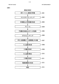
Various techniques can be employed to enhance the efficiency of p-n junctions in solar cell applications. These include optimizing the doping concentration, improving the junction formation process, and reducing recombination losses at the junction interface. By carefully controlling these parameters, the conversion efficiency of solar cells can be significantly increased, leading to better performance in photovoltaic applications.- Semiconductor material selection for P-N junction efficiency: The choice of semiconductor materials significantly impacts P-N junction efficiency. Various materials with specific band gaps and carrier mobilities can be selected to optimize energy conversion. Advanced materials such as gallium arsenide, silicon carbide, and perovskites offer improved electron-hole pair generation and reduced recombination losses. Material purity and crystalline structure also play crucial roles in enhancing junction performance and overall efficiency.
- Junction design optimization techniques: Optimizing P-N junction design involves careful engineering of junction depth, doping profiles, and interface characteristics. Techniques such as gradient doping, selective emitter structures, and passivation layers can reduce recombination losses at the junction interface. Advanced junction architectures including heterojunctions and multi-junction designs distribute the electromagnetic spectrum more effectively, leading to higher conversion efficiencies and better performance under various operating conditions.
- Surface treatment and passivation methods: Surface treatment and passivation techniques significantly enhance P-N junction efficiency by reducing surface recombination velocities. Methods include chemical passivation, thermal oxidation, atomic layer deposition, and application of specialized coatings. These treatments neutralize dangling bonds at interfaces, minimize defect states, and create electric fields that repel minority carriers from surfaces. Effective passivation leads to increased carrier lifetimes and improved collection efficiency.
- Testing and measurement systems for junction efficiency: Advanced testing and measurement systems are essential for accurately evaluating P-N junction efficiency. These include quantum efficiency measurements, electroluminescence imaging, photoluminescence spectroscopy, and current-voltage characteristic analysis. Real-time monitoring systems can detect performance degradation and identify specific loss mechanisms. Standardized testing protocols ensure reliable comparison between different junction designs and materials, facilitating continuous improvement in efficiency.
- Novel device structures for enhanced efficiency: Innovative device structures can significantly improve P-N junction efficiency. These include tandem architectures, interdigitated back contact designs, and tunnel junction implementations. Three-dimensional junction structures increase the effective surface area for light absorption while minimizing carrier transport distances. Micro and nano-structured surfaces enhance light trapping capabilities. Integration of quantum dots, nanowires, and plasmonic structures further improves light absorption and carrier collection efficiency.
02 Novel P-N Junction Structures for Enhanced Performance
Advanced p-n junction structures have been developed to improve efficiency in semiconductor devices. These include heterojunctions, multi-junction designs, and nanostructured junctions that can better capture and convert light energy. The innovative junction architectures help to overcome traditional limitations of conventional p-n junctions by optimizing band alignment, reducing interface defects, and enhancing carrier collection.Expand Specific Solutions03 Measurement and Testing Methods for P-N Junction Efficiency
Specialized techniques and equipment have been developed for accurately measuring and testing p-n junction efficiency. These methods include advanced characterization tools, simulation models, and testing protocols that can precisely evaluate junction performance parameters such as carrier lifetime, quantum efficiency, and fill factor. Accurate measurement is crucial for optimizing junction design and manufacturing processes.Expand Specific Solutions04 Material Innovations for High-Efficiency P-N Junctions
Novel materials and material combinations are being utilized to create high-efficiency p-n junctions. These include advanced semiconductor compounds, organic semiconductors, and hybrid materials that offer superior electrical properties. The selection and engineering of these materials can significantly impact junction performance by improving carrier mobility, reducing defects, and enhancing light absorption capabilities.Expand Specific Solutions05 Manufacturing Processes for Efficient P-N Junctions
Innovative manufacturing techniques have been developed to produce high-efficiency p-n junctions with improved consistency and reduced defects. These processes include advanced deposition methods, precise doping techniques, and novel annealing procedures that can create junctions with optimal electrical characteristics. Manufacturing innovations focus on creating cleaner interfaces, more uniform doping profiles, and better crystalline quality to maximize junction efficiency.Expand Specific Solutions
Leading Solar Cell Manufacturers and Research Institutions
The P-N junction efficiency enhancement for solar cells is currently in a mature development phase, with significant market growth driven by increasing renewable energy demands. The market size is expanding rapidly, expected to reach substantial value as solar technology becomes more mainstream. Technologically, advancements are occurring at varying rates across key players. The University of California and Tsinghua University lead academic research with breakthrough junction designs, while Samsung Electronics, Applied Materials, and Aiko Solar demonstrate industrial maturity through mass-production innovations. Companies like JinkoSolar and Canadian Solar (CSI Cells) have achieved commercial-scale implementation of enhanced P-N junction technologies. The competitive landscape shows collaboration between research institutions and manufacturers, with specialized players like Soitec and 3SUN focusing on novel substrate technologies that further improve junction efficiency.
Samsung SDI Co., Ltd.
Technical Solution: Samsung SDI has developed proprietary PERC (Passivated Emitter and Rear Cell) technology with advanced P-N junction optimization. Their approach incorporates rear-side passivation layers with locally opened contact areas, significantly reducing electron-hole recombination at the back surface. Samsung's innovation includes a specialized aluminum oxide/silicon nitride stack that provides exceptional surface passivation while simultaneously acting as an effective rear reflector, increasing light trapping within the cell. Their manufacturing process employs precision laser ablation techniques to create selective openings in the dielectric layer with positioning accuracy of ±5μm, enabling optimal contact formation without compromising passivation quality. Samsung SDI has further enhanced junction efficiency through implementation of multi-busbar technology with round wires that minimize shading losses while improving current collection. Recent developments include integration of gallium doping in the P-type base to mitigate light-induced degradation, resulting in more stable P-N junction performance throughout the cell's operational lifetime.
Strengths: Exceptional manufacturing quality control; vertical integration allowing for coordinated improvements across materials and processes; strong expertise in mass production scaling. Weaknesses: Higher production costs compared to conventional Al-BSF cells; increased process complexity requiring more sophisticated manufacturing equipment; technology primarily optimized for monocrystalline silicon substrates rather than multi-crystalline materials.
Tsinghua University
Technical Solution: Tsinghua University has pioneered several breakthrough approaches to P-N junction optimization for solar cells. Their research team has developed a novel heterojunction architecture utilizing transition metal oxide layers as selective contacts, demonstrating a significant reduction in interface recombination velocity (below 10 cm/s). Their proprietary two-step annealing process creates a carefully engineered dopant profile that maximizes the built-in potential while minimizing Auger recombination effects. Tsinghua researchers have implemented advanced surface passivation using atomic layer deposition of Al2O3 with precisely controlled thickness (10-15nm), achieving surface recombination velocities below 5 cm/s on both n-type and p-type surfaces. Their innovative approach to junction formation includes quantum dot sensitization at the interface, which enhances light absorption in the near-infrared region while maintaining excellent electronic properties. Recent publications demonstrate their success with a hybrid passivation scheme combining chemical and field-effect passivation mechanisms, resulting in an impressive open-circuit voltage improvement of 25-30mV compared to conventional approaches. Tsinghua's work on defect engineering through controlled introduction of hydrogen has shown remarkable ability to neutralize recombination centers throughout the junction region.
Strengths: Cutting-edge fundamental research capabilities; access to advanced characterization techniques allowing detailed understanding of junction physics; strong collaboration network with manufacturing partners. Weaknesses: Some technologies remain at laboratory scale with challenges for mass production implementation; higher material costs for certain advanced architectures; some approaches require ultra-high purity materials that increase overall costs.
Key Patents in P-N Junction Enhancement
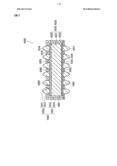
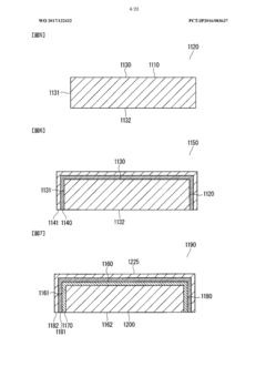
Solar Cell and Method of Fabricating the Same
PatentInactiveEP2312650A2
Innovation
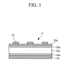
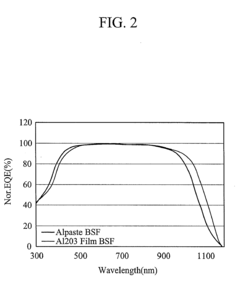
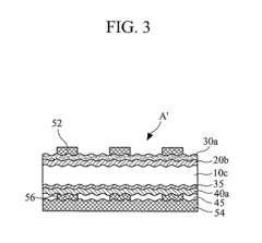
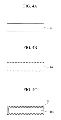
- A solar cell with a back surface field (BSF) layer formed using AlO, AlN, or AlON films, which have a Negative Fixed Charge (NFC) characteristic, is used to prevent recombination and enhance internal reflection, thereby increasing the lifetime of electron-hole pairs and improving the opto-electric conversion efficiency.
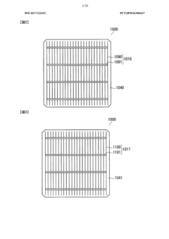
Solar cell and method for producing solar cell
PatentWO2017122422A1
Innovation
- A solar cell design where the end face of the pn junction is covered with a dielectric film containing aluminum oxide, and the main surface of the p-n junction exhibiting n-type conductivity is covered without aluminum oxide, allowing for a silver-containing electrode to make contact without increased resistance.
Materials Science Innovations for Solar Cells
Recent advancements in materials science have revolutionized solar cell technology, particularly in enhancing P-N junction efficiency. Traditional silicon-based solar cells have reached theoretical efficiency limits, prompting researchers to explore novel materials and structures. Perovskite materials have emerged as promising candidates, demonstrating remarkable photovoltaic properties with tunable bandgaps that allow for optimal solar spectrum absorption.
Tandem solar cell architectures incorporating multiple materials with complementary absorption spectra have shown significant efficiency improvements. These multi-junction designs leverage different bandgap materials to capture broader portions of the solar spectrum, with recent perovskite-silicon tandems achieving efficiencies exceeding 29%, substantially higher than single-junction silicon cells.
Nanostructured materials represent another frontier in solar cell development. Quantum dots, nanowires, and 2D materials like graphene and transition metal dichalcogenides offer unique electronic properties that can enhance charge separation and transport at P-N junctions. These nanomaterials enable precise bandgap engineering and improved carrier mobility, addressing fundamental efficiency limitations.
Surface passivation techniques have advanced significantly, with atomic layer deposition methods allowing for nanometer-precision coating of interface materials that reduce recombination losses. Novel passivation materials such as aluminum oxide and hafnium oxide have demonstrated exceptional surface defect mitigation properties, directly enhancing P-N junction performance.
Transparent conducting oxides (TCOs) have evolved to provide better electrical conductivity while maintaining high optical transparency. Materials like indium tin oxide (ITO) alternatives, including fluorine-doped tin oxide and zinc oxide doped with aluminum, offer improved performance with reduced material costs and environmental impact.
Back-contact designs eliminate front-surface shadowing losses by relocating electrical contacts to the rear of the cell. This innovation, combined with advanced materials, has enabled record-breaking efficiencies in certain cell architectures by maximizing the active light-absorbing area and improving carrier collection efficiency.
Emerging materials for carrier-selective contacts, such as transition metal oxides and organic semiconductors, provide enhanced carrier selectivity at P-N junctions. These materials create asymmetric energy barriers that facilitate efficient extraction of one carrier type while blocking the other, significantly reducing interface recombination losses that traditionally limit junction efficiency.
Environmental Impact and Sustainability Considerations
The enhancement of P-N junction efficiency in solar cells carries significant environmental implications that extend beyond mere technical performance metrics. Solar energy represents one of the cleanest renewable energy sources available, with the potential to substantially reduce greenhouse gas emissions compared to fossil fuel-based electricity generation. Improving P-N junction efficiency directly contributes to this environmental benefit by enabling greater energy harvest from the same physical footprint, thereby accelerating the displacement of carbon-intensive energy sources.
Manufacturing processes for high-efficiency P-N junctions often involve energy-intensive steps and potentially hazardous materials. Traditional silicon purification requires temperatures exceeding 1400°C, consuming substantial energy and generating significant carbon emissions during production. Advanced junction technologies may incorporate rare earth elements or toxic compounds such as cadmium telluride, raising concerns about resource depletion and end-of-life disposal. Sustainable enhancement strategies must therefore consider the full lifecycle environmental impact, not merely operational efficiency.
Water usage represents another critical environmental consideration, particularly for manufacturing facilities located in water-stressed regions. Semiconductor fabrication processes typically require ultra-pure water for cleaning and processing, with some estimates suggesting that producing a single silicon wafer may consume thousands of liters of water. Efficiency enhancements that reduce material requirements could proportionally decrease this water footprint.
The longevity and degradation characteristics of enhanced P-N junctions also factor into sustainability assessments. Technologies that extend operational lifetimes from the current industry standard of 25-30 years to 40+ years would significantly improve lifecycle carbon metrics and reduce electronic waste generation. Conversely, certain high-efficiency junction designs may accelerate degradation under field conditions, potentially undermining long-term sustainability benefits despite initial performance advantages.
Recycling considerations must be integrated into P-N junction development pathways. Current solar panel recycling rates remain suboptimal, with many end-of-life panels entering landfills. Novel junction architectures incorporating easily separable layers or avoiding difficult-to-recycle composite materials could facilitate more effective material recovery. This circular economy approach would reduce primary resource demands and minimize waste generation across the technology lifecycle.
Energy payback time—the period required for a solar cell to generate the energy consumed during its production—serves as a critical sustainability metric for enhanced P-N junctions. Current silicon-based technologies typically achieve energy payback within 1-4 years depending on installation location. Junction efficiency improvements that reduce material requirements or simplify manufacturing could potentially lower this figure to under one year, dramatically improving the net environmental benefit of solar deployment.
Unlock deeper insights with Patsnap Eureka Quick Research — get a full tech report to explore trends and direct your research. Try now!
Generate Your Research Report Instantly with AI Agent
Supercharge your innovation with Patsnap Eureka AI Agent Platform!