

Analyze P–N Junction Formation Techniques for IC Fabrication
SEP 12, 20259 MIN READ
Generate Your Research Report Instantly with AI Agent
PatSnap Eureka helps you evaluate technical feasibility & market potential.
P-N Junction Technology Background and Objectives
The P-N junction represents one of the most fundamental building blocks in semiconductor device physics and integrated circuit (IC) fabrication. Since its theoretical conception in the 1930s and practical implementation in the 1940s, P-N junction technology has undergone remarkable evolution, transforming from discrete components to highly sophisticated structures integrated within modern nanoscale ICs.
The historical trajectory of P-N junction development began with the pioneering work of Russell Ohl at Bell Laboratories, who discovered the photovoltaic effect at semiconductor junctions in 1939. This was followed by the invention of the first transistor in 1947, which relied critically on P-N junction physics. The subsequent decades witnessed progressive refinements in junction formation techniques, moving from alloying methods to diffusion processes, and eventually to ion implantation approaches.
Current technological trends in P-N junction formation are primarily driven by the semiconductor industry's relentless pursuit of device miniaturization according to Moore's Law, while simultaneously addressing challenges related to power consumption, thermal management, and manufacturing yield. The industry is witnessing a shift toward ultra-shallow junctions with precisely controlled doping profiles to accommodate sub-10nm technology nodes.
The primary technical objectives in modern P-N junction formation include achieving atomically abrupt junction interfaces, minimizing defect densities, ensuring uniform doping distributions, and developing processes compatible with three-dimensional device architectures. Additionally, there is growing emphasis on techniques that can operate at lower thermal budgets to prevent dopant diffusion and maintain the integrity of previously fabricated structures.
Another critical objective is the development of junction formation methods compatible with new semiconductor materials beyond silicon, including silicon-germanium, III-V compounds, and wide-bandgap semiconductors like silicon carbide and gallium nitride. These materials promise enhanced device performance but present unique challenges for creating high-quality P-N junctions.
Looking forward, the field is exploring novel approaches such as monolayer doping, laser annealing, and plasma-based techniques to overcome the limitations of conventional junction formation methods. Concurrently, there is increasing interest in leveraging quantum effects at nanoscale junctions to develop next-generation devices with unprecedented functionality.
The ultimate goal of P-N junction technology advancement is to enable the continued scaling of semiconductor devices while improving performance, reducing power consumption, and enhancing reliability—all critical factors for supporting emerging applications in artificial intelligence, quantum computing, 5G communications, and Internet of Things (IoT) devices.
Market Analysis for P-N Junction Applications
The global market for P-N junction applications continues to expand significantly, driven by the increasing demand for semiconductor devices across various industries. The integrated circuit (IC) market, where P-N junctions serve as fundamental building blocks, is projected to reach $803.2 billion by 2028, growing at a CAGR of 8.2% from 2023. This growth is primarily fueled by the rising adoption of electronic devices in automotive, consumer electronics, telecommunications, and industrial automation sectors.
Within the semiconductor industry, P-N junction-based devices account for approximately 65% of the total market share, highlighting their critical importance in modern electronics. Power electronics, which heavily rely on P-N junction technology, represent a particularly fast-growing segment with a market value of $42.7 billion in 2022 and expected to reach $63.1 billion by 2027.
The demand for more efficient P-N junction formation techniques is being driven by several market factors. Miniaturization trends in electronics have created a need for more precise junction formation methods, as device dimensions continue to shrink below 5nm. This has led to increased investment in advanced doping technologies, with the ion implantation equipment market alone valued at $12.4 billion in 2022.
Regional analysis reveals that Asia-Pacific dominates the market for P-N junction applications, accounting for 58% of global production, with particular concentration in Taiwan, South Korea, and China. North America follows with 22% market share, focusing primarily on high-performance computing and specialized applications. Europe represents 15% of the market, with strength in automotive and industrial applications.
The market is also witnessing a shift toward compound semiconductor materials for P-N junction formation. Silicon carbide (SiC) and gallium nitride (GaN) based devices are experiencing rapid growth rates of 25% and 30% respectively, driven by their superior performance in high-power and high-frequency applications. This trend is creating new market opportunities for specialized P-N junction formation techniques tailored to these materials.
Consumer demand for energy-efficient devices is another significant market driver, with power management ICs experiencing 12% annual growth. This has intensified research into junction formation techniques that minimize leakage current and improve overall device efficiency. Similarly, the expanding electric vehicle market, growing at 24% annually, is creating substantial demand for power semiconductor devices with optimized P-N junctions for high-voltage applications.
The increasing focus on renewable energy systems has also opened new market avenues for P-N junction applications, particularly in photovoltaic cells and power conversion systems, with the solar inverter market alone expected to reach $27.2 billion by 2026.
Current P-N Junction Formation Challenges
Despite significant advancements in semiconductor fabrication, P-N junction formation continues to face several critical challenges that impede further progress in integrated circuit miniaturization and performance enhancement. The most pressing issue remains the precise control of dopant profiles at nanoscale dimensions. As device geometries shrink below 5nm, conventional diffusion-based doping methods struggle to maintain abrupt junction profiles, leading to unwanted dopant spreading and junction depth variations that compromise device performance.
Thermal budget constraints present another significant hurdle. Traditional annealing processes required for dopant activation often cause undesired dopant diffusion, particularly problematic in ultra-shallow junction formation. The industry faces a fundamental trade-off between sufficient dopant activation and maintaining sharp junction profiles, with higher temperatures improving activation but degrading junction abruptness.
Ion implantation damage recovery represents a persistent challenge. The crystal lattice damage caused during implantation requires annealing for repair, yet complete damage elimination without compromising junction characteristics remains difficult. Residual defects can create leakage paths and degrade carrier mobility, directly impacting device performance and reliability.
The integration of novel materials further complicates junction formation. As silicon-based technologies approach physical limits, alternative materials like SiGe, III-V compounds, and 2D materials are being explored. However, forming consistent, high-quality P-N junctions in these materials presents unique challenges due to different dopant solubilities, activation energies, and diffusion behaviors compared to silicon.
Metrology and characterization limitations also hinder progress. Current analytical techniques struggle to provide accurate, non-destructive measurements of dopant profiles at nanometer scales. This measurement gap creates difficulties in process development and quality control, as engineers cannot precisely verify the junction characteristics they aim to achieve.
Manufacturing scalability remains problematic for advanced junction formation techniques. While methods like molecular layer doping and monolayer doping offer promising solutions for ultra-shallow junctions, their integration into high-volume manufacturing environments presents significant challenges related to throughput, uniformity, and cost-effectiveness.
Finally, the industry faces increasing challenges in meeting power and performance requirements simultaneously. As devices scale down, junction-related parasitic resistances and capacitances become increasingly dominant factors limiting circuit performance. Balancing low junction resistance with minimal leakage current becomes exponentially more difficult at advanced technology nodes, requiring innovative approaches to junction engineering.
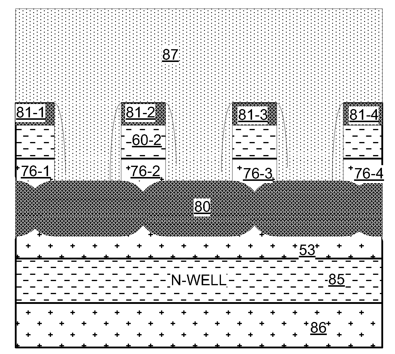
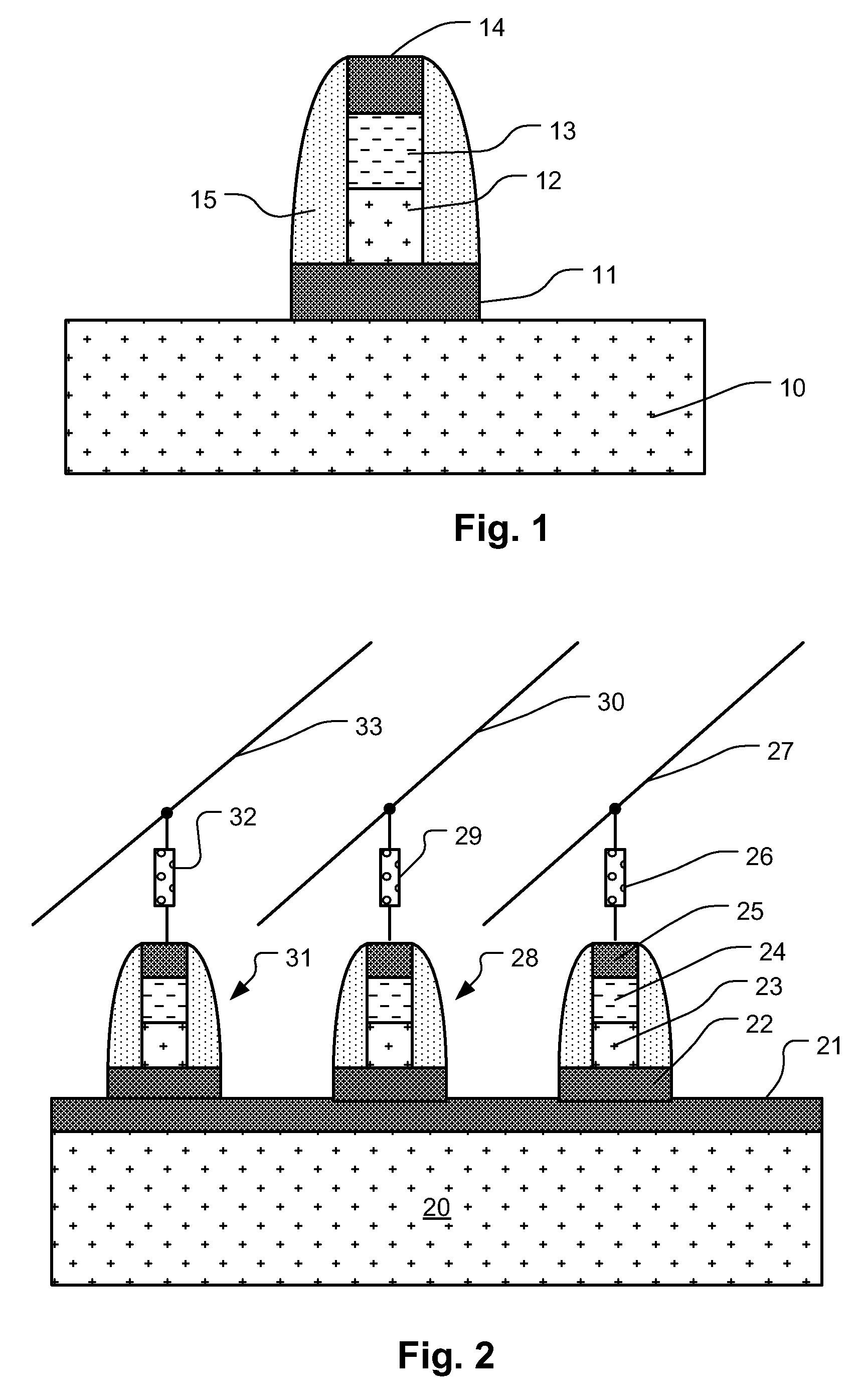
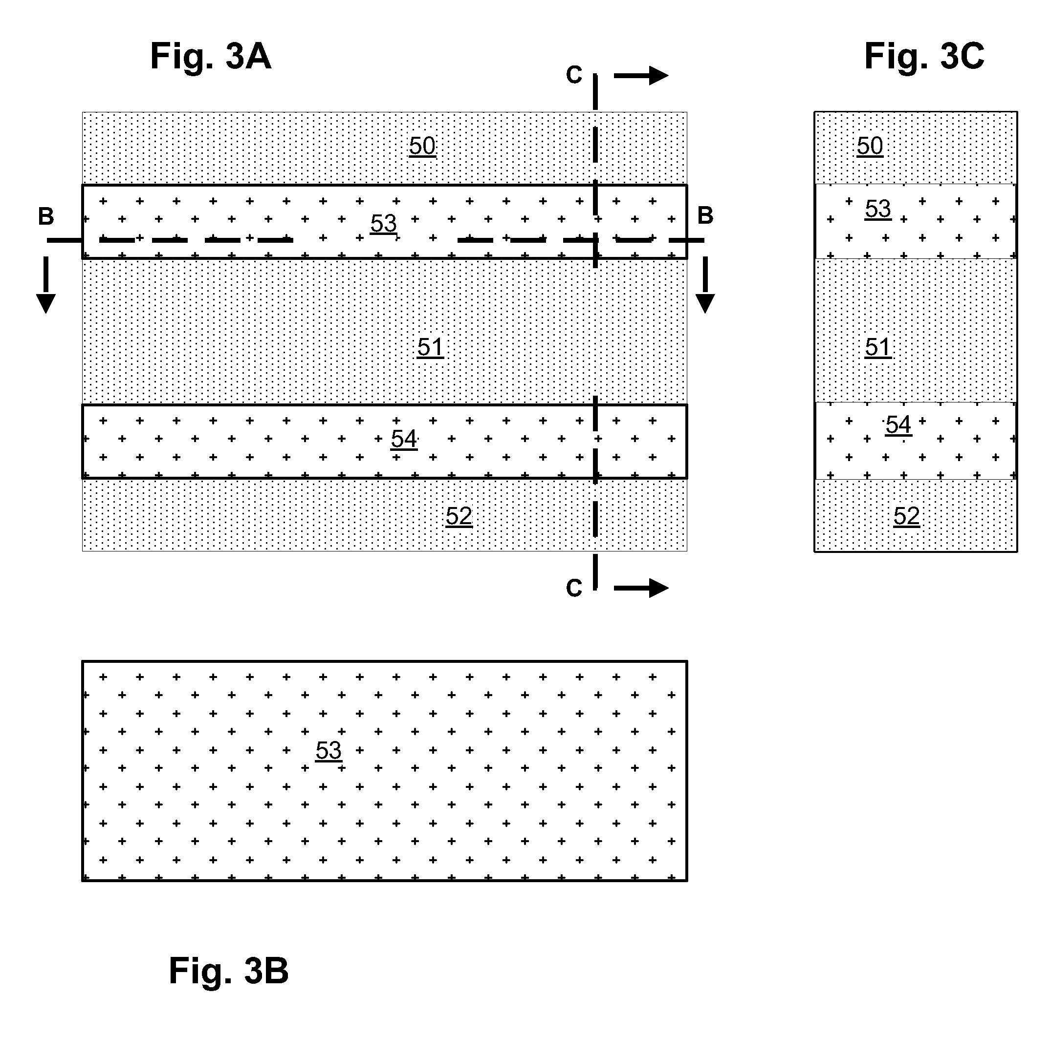
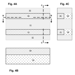
Current P-N Junction Fabrication Techniques
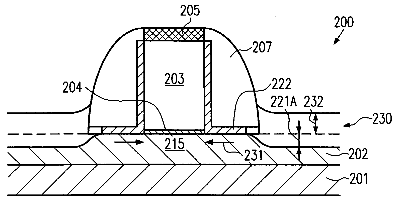
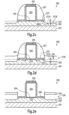
01 Diffusion-based P-N Junction Formation
Diffusion is a traditional technique for forming P-N junctions in semiconductor devices. This process involves the controlled diffusion of dopant atoms into a semiconductor substrate at high temperatures. The dopant atoms move from regions of high concentration to regions of low concentration, creating a junction between p-type and n-type regions. This technique allows for precise control of junction depth and dopant concentration profiles, which are critical for device performance.- Diffusion-based P-N Junction Formation: Diffusion is a traditional technique for forming P-N junctions where dopant atoms are introduced into a semiconductor substrate through thermal processes. This method involves heating the semiconductor material to high temperatures to allow dopant atoms to diffuse into the crystal lattice, creating regions with different conductivity types. The depth and concentration profile of the junction can be controlled by adjusting the diffusion temperature, time, and dopant concentration.
- Ion Implantation Techniques: Ion implantation is a precise method for P-N junction formation where dopant ions are accelerated at high energy and implanted into the semiconductor substrate. This technique offers better control over dopant concentration and junction depth compared to diffusion methods. The process typically requires a subsequent annealing step to repair crystal damage and activate the implanted dopants. Ion implantation allows for selective doping through the use of masks and enables the creation of complex junction profiles.
- Epitaxial Growth for Junction Formation: Epitaxial growth techniques involve the deposition of crystalline semiconductor layers on a substrate to form P-N junctions. This method allows for precise control of layer thickness and dopant concentration, enabling the creation of high-quality junctions with abrupt transitions. Various epitaxial techniques include vapor phase epitaxy (VPE), molecular beam epitaxy (MBE), and metal-organic chemical vapor deposition (MOCVD). These methods are particularly important for advanced semiconductor devices requiring precise junction characteristics.
- Novel Junction Formation for Advanced Devices: Advanced techniques for P-N junction formation include heterojunction formation, quantum well structures, and nanoscale junction engineering. These methods often combine different semiconductor materials to create junctions with unique electrical and optical properties. Novel approaches include selective area growth, atomic layer deposition, and laser-assisted doping. These techniques are particularly important for optoelectronic devices, high-frequency transistors, and power electronics where conventional junction formation methods may be inadequate.
- Junction Formation in Special Semiconductor Materials: P-N junction formation in non-silicon materials such as compound semiconductors (GaAs, InP, GaN), wide bandgap semiconductors (SiC, diamond), and emerging 2D materials requires specialized techniques. These materials often demand unique processing conditions due to their different crystal structures, thermal properties, and chemical characteristics. Techniques include specialized annealing processes, surface treatments, and custom dopant selection to achieve optimal junction characteristics while minimizing defects and maintaining material integrity.
02 Ion Implantation Techniques
Ion implantation is a modern technique for P-N junction formation that offers superior control over dopant profiles compared to diffusion. In this process, ionized dopant atoms are accelerated in an electric field and directed into the semiconductor substrate. The energy of the ions determines their penetration depth, allowing for precise placement of dopants. Post-implantation annealing is typically required to repair crystal damage and activate the dopants. This technique enables the formation of shallow junctions needed for advanced semiconductor devices.Expand Specific Solutions03 Epitaxial Growth Methods
Epitaxial growth involves the deposition of a crystalline layer on a crystalline substrate, where the deposited layer maintains the crystal structure of the substrate. For P-N junction formation, epitaxial layers with different dopant types can be grown sequentially to create the junction. Techniques such as chemical vapor deposition (CVD), molecular beam epitaxy (MBE), and liquid phase epitaxy (LPE) are commonly used. This approach allows for the creation of abrupt junctions with minimal defects and precise control over layer thickness.Expand Specific Solutions04 Selective Area Doping
Selective area doping techniques enable the formation of P-N junctions in specific regions of a semiconductor substrate. This is typically achieved using masks or barriers that prevent dopant incorporation in protected areas. Methods include selective diffusion, masked ion implantation, and selective epitaxial growth. These techniques are essential for creating complex device structures with multiple P-N junctions in integrated circuits, allowing for the fabrication of transistors, diodes, and other semiconductor components with specific electrical characteristics.Expand Specific Solutions05 Advanced Junction Engineering
Advanced junction engineering encompasses novel techniques for optimizing P-N junction properties beyond traditional methods. These include the formation of graded junctions with varying dopant concentrations, heterojunctions between different semiconductor materials, and ultra-shallow junctions for nanoscale devices. Techniques such as rapid thermal annealing, laser annealing, and solid phase epitaxy are employed to achieve precise dopant activation and distribution. These advanced methods enable the development of high-performance semiconductor devices with improved electrical characteristics.Expand Specific Solutions
Key Semiconductor Industry Players
P-N junction formation techniques for IC fabrication are currently in a mature development stage, with the market expected to grow steadily due to increasing semiconductor demand. The global market is substantial, driven by applications in power electronics, optoelectronics, and integrated circuits. Leading players include Taiwan Semiconductor Manufacturing Co. (TSMC) and Samsung Electronics, who have established advanced junction formation processes at commercial scale. Applied Materials and IBM provide critical equipment and research innovations, while academic institutions like California Institute of Technology and University of Electronic Science & Technology of China contribute fundamental research. Renesas Electronics and Infineon Technologies Austria specialize in power semiconductor applications, demonstrating the technology's commercial viability across multiple sectors. The technology continues to evolve toward more precise, efficient junction formation methods.
Mitsubishi Electric Corp.
Technical Solution: Mitsubishi Electric has developed specialized P-N junction formation techniques primarily focused on power semiconductor applications. Their approach centers on deep junction formation with precisely controlled doping profiles to achieve optimal breakdown voltage and on-resistance characteristics. For their IGBT (Insulated Gate Bipolar Transistor) products, Mitsubishi employs a multi-energy ion implantation process combined with long thermal diffusion cycles to create carefully engineered field-stop layers and collector regions[1]. Their SiC (Silicon Carbide) power device manufacturing incorporates high-temperature ion implantation above 500°C to reduce lattice damage during the doping process, followed by ultra-high temperature annealing (>1600°C) for dopant activation[3]. Mitsubishi has pioneered the use of aluminum ion implantation for p-type regions in SiC devices, achieving controlled junction depths despite aluminum's challenging diffusion characteristics. For their advanced power MOSFETs, Mitsubishi utilizes a proprietary super-junction formation technique involving multiple epitaxial growth and implantation steps to create vertically aligned P-N columns that optimize the electric field distribution throughout the device structure[4].
Strengths: Industry-leading expertise in power semiconductor junction engineering; excellent control of deep junction profiles; advanced capabilities in wide-bandgap semiconductor doping. Weaknesses: Processes optimized for power applications have limited applicability to logic/memory devices; long thermal cycles increase manufacturing time; some techniques require specialized high-temperature equipment.
Samsung Electronics Co., Ltd.
Technical Solution: Samsung has developed sophisticated P-N junction formation techniques for their advanced semiconductor manufacturing processes. Their approach combines high-precision ion implantation with innovative annealing strategies tailored for different device architectures. For their advanced logic nodes, Samsung employs cluster ion implantation with molecular dopant species to achieve ultra-shallow junctions with minimal end-of-range defects[2]. Their process incorporates millisecond annealing technologies, including dynamic surface annealing (DSA) and laser spike annealing (LSA), which provide excellent dopant activation while maintaining abrupt junction profiles with depths below 10nm[3]. For 3D device structures like FinFETs and GAA transistors, Samsung has pioneered conformal doping techniques using plasma doping (PLAD) combined with specialized annealing sequences to ensure uniform junction formation on vertical surfaces. Their DRAM manufacturing employs tailored junction engineering with precisely controlled phosphorus and boron profiles to optimize cell transistor performance. Samsung has also developed specialized junction formation processes for their V-NAND technology, incorporating epitaxial growth techniques for precise dopant incorporation in complex 3D structures[5].
Strengths: Excellent integration of junction formation techniques with diverse product technologies (logic, memory, storage); advanced capabilities in 3D structure doping; sophisticated process control systems ensuring manufacturing consistency. Weaknesses: Complex multi-step processes increase production cycle time; specialized equipment requirements add to manufacturing costs; some techniques face scaling challenges at the most advanced nodes.
Critical Patents in P-N Junction Formation
Advanced technique for forming a transistor having raised drain and source regions
PatentInactiveUS20050093075A1
Innovation
- The introduction of a strain layer during epitaxial growth in the drain and source regions, or by modifying the dopant profile, allows for enhanced channel conductivity without adverse effects on the dopant profile or channel length, using a replaceable mask or spacer to control the recess formation and epitaxial growth process.
Integrated circuit device with single crystal silicon on silicide and manufacturing method
PatentActiveUS20100171188A1
Innovation
- A manufacturing method involving a silicide element on a silicon substrate with a single crystal silicon node, where the silicide separates the node from the substrate, and additional semiconductor nodes are formed to create diodes or transistors, using a silicide precursor that reacts with the silicon body to form a conductive path while maintaining the single crystal state.
Materials Science Advancements for Junction Quality
Recent advancements in materials science have significantly enhanced P-N junction quality in integrated circuit fabrication. The introduction of high-purity semiconductor materials, particularly silicon with defect densities below 1 part per billion, has dramatically improved junction characteristics. These ultra-pure materials minimize unwanted impurities that can cause leakage currents and reduce device performance, enabling the creation of more precise and efficient junctions.
Strain engineering has emerged as a critical technique for junction quality enhancement. By deliberately introducing strain into the crystal lattice, researchers have successfully modified band structures and carrier mobilities. Compressive strain in P-type regions and tensile strain in N-type regions have shown up to 45% improvement in carrier transport properties, directly translating to better junction performance and reduced power consumption in modern ICs.
Novel dopant materials beyond traditional boron and phosphorus have expanded the designer's toolkit. Elements such as carbon, germanium, and various rare earth metals are being incorporated to fine-tune junction properties. These alternative dopants offer advantages in diffusion control, activation efficiency, and thermal stability, particularly important as device dimensions continue to shrink below 5nm.
Two-dimensional materials represent a revolutionary frontier in junction formation. Materials like graphene, transition metal dichalcogenides (TMDs), and hexagonal boron nitride (h-BN) exhibit exceptional electronic properties at atomic thicknesses. Heterojunctions created with these 2D materials demonstrate nearly ideal diode characteristics with minimal defect-related issues, potentially enabling a new generation of ultra-thin, flexible electronic devices.
Interface engineering techniques have advanced considerably, focusing on the critical boundary between P and N regions. Atomic layer deposition (ALD) and molecular beam epitaxy (MBE) now allow atomic-level control over interface composition. This precision has reduced interface trap densities by over 90% compared to conventional methods, minimizing recombination losses and enhancing overall junction efficiency.
Temperature-controlled processing innovations have expanded the thermal budget flexibility for junction formation. Low-temperature processes (below 600°C) using microwave-assisted annealing and flash lamp annealing enable junction formation in temperature-sensitive materials and structures. These techniques have proven particularly valuable for 3D integrated circuits and flexible electronics applications where traditional high-temperature processes would damage underlying layers.
Environmental Impact of Junction Formation Processes
The environmental impact of P-N junction formation processes in IC fabrication has become increasingly significant as semiconductor manufacturing scales globally. Traditional junction formation techniques, particularly those involving high-temperature diffusion and ion implantation, consume substantial energy resources. A typical semiconductor fabrication facility utilizing these processes may consume electricity equivalent to a small city, with junction formation steps accounting for approximately 15-20% of the total energy footprint.
Chemical usage presents another critical environmental concern. Dopant sources often contain toxic elements such as arsenic, phosphorus, and boron compounds. When improperly handled or disposed of, these materials pose significant risks to soil and groundwater systems. Modern fabrication facilities generate between 500-1000 liters of contaminated wastewater per wafer processed, with junction formation processes contributing substantially to this volume.
Gaseous emissions from junction formation processes include volatile organic compounds (VOCs), perfluorocarbons (PFCs), and other greenhouse gases with high global warming potential. Ion implantation systems, widely used for precise junction formation, utilize gases like arsine and phosphine that are both highly toxic and environmentally persistent. The semiconductor industry's contribution to atmospheric fluorinated compound emissions has been estimated at 3-4% of total industrial emissions.
Recent advancements in green manufacturing techniques show promising developments. Laser annealing methods reduce thermal budget requirements by up to 60% compared to conventional furnace processes. Solid-source diffusion techniques minimize hazardous waste generation by eliminating many liquid dopant sources. Additionally, plasma doping (PLAD) technologies have demonstrated up to 30% reduction in process gas consumption compared to traditional beam-line implantation.
Regulatory frameworks worldwide have increasingly focused on semiconductor manufacturing environmental impacts. The European Union's Restriction of Hazardous Substances (RoHS) directive and similar regulations in Asia have driven manufacturers to develop junction formation processes with reduced environmental footprints. Leading semiconductor companies have responded by implementing closed-loop water recycling systems that recover up to 85% of process water.
Life cycle assessment studies indicate that environmental impacts extend beyond manufacturing to end-of-life considerations. The difficulty in separating and recovering dopant materials from semiconductor waste contributes to electronic waste challenges. Emerging circular economy approaches focus on designing junction formation processes that facilitate eventual material recovery and reuse, though these remain in early development stages.
Unlock deeper insights with PatSnap Eureka Quick Research — get a full tech report to explore trends and direct your research. Try now!
Generate Your Research Report Instantly with AI Agent
Supercharge your innovation with PatSnap Eureka AI Agent Platform!