

Comparing P–N Junction Types: Which Delivers Higher Output?
SEP 4, 202510 MIN READ
Generate Your Research Report Instantly with AI Agent
Patsnap Eureka helps you evaluate technical feasibility & market potential.
P-N Junction Technology Background and Objectives
P-N junction technology has evolved significantly since its discovery in the early 20th century, representing one of the fundamental building blocks of modern semiconductor devices. The development trajectory began with the theoretical work of Walter Schottky and Nevill Mott in the 1930s, followed by practical implementation at Bell Laboratories in the 1940s. This technology has since undergone continuous refinement, with various junction types emerging to address specific application requirements across multiple industries.
The evolution of P-N junction technology has been characterized by progressive improvements in efficiency, reliability, and output capacity. Traditional homojunction designs have given way to more sophisticated heterojunction and multi-junction architectures, each offering distinct performance characteristics. These advancements have been driven by the growing demand for higher energy conversion efficiency, particularly in photovoltaic applications and power electronics.
Current technological trends indicate a shift toward optimizing junction performance through novel materials, innovative fabrication techniques, and advanced doping methodologies. The integration of nanotechnology has further expanded the possibilities for junction design, enabling unprecedented control over carrier transport and recombination processes. These developments have significantly influenced the output capabilities of different junction types, creating a complex landscape of performance trade-offs.
The primary objective of this technical research is to conduct a comprehensive comparative analysis of various P-N junction types, with particular emphasis on their output performance metrics. This investigation aims to identify which junction configurations deliver superior output under different operating conditions, considering factors such as temperature sensitivity, radiation hardness, and long-term stability. The research will evaluate homojunctions, heterojunctions, graded junctions, and multi-junction structures across relevant performance parameters.
Additionally, this research seeks to establish quantifiable benchmarks for junction performance that can guide future development efforts. By systematically analyzing the relationship between junction design parameters and output characteristics, we aim to develop predictive models that can accelerate the optimization process for specific applications. This approach will help bridge the gap between theoretical understanding and practical implementation of high-performance junction technologies.
The findings from this research will provide valuable insights for industries reliant on semiconductor technologies, particularly those focused on energy conversion, signal processing, and power management. By clarifying which junction types excel in specific operational contexts, this research will support more informed decision-making in technology selection and development strategies for next-generation electronic devices and systems.
Market Applications and Demand Analysis
The global market for P-N junction technologies continues to expand rapidly, driven by increasing demand across multiple sectors. The semiconductor industry, valued at approximately $573 billion in 2022, relies heavily on various P-N junction configurations to meet diverse application requirements. Market analysis reveals that the choice between different P-N junction types significantly impacts product performance and market positioning.
Consumer electronics represents the largest application segment, with smartphones alone accounting for over 1.4 billion units shipped annually. In this sector, manufacturers prioritize P-N junction configurations that maximize energy efficiency while maintaining compact form factors. High-output junction designs command premium pricing, particularly in flagship devices where performance differentiation is crucial for market success.
The renewable energy sector presents perhaps the most compelling case for high-output P-N junctions. The global solar photovoltaic market, growing at 20% annually, demands increasingly efficient semiconductor junctions to improve conversion rates. Market data indicates that even marginal improvements in junction efficiency translate to substantial competitive advantages, with consumers willing to pay 15-25% premiums for panels offering higher energy output.
Automotive applications represent another high-growth segment, particularly with electric vehicles reaching 10% of global vehicle sales. Advanced driver assistance systems and power management modules require specialized P-N junctions optimized for reliability under variable temperature conditions. Market research indicates automotive-grade semiconductors with higher output capabilities command significant price premiums due to their performance advantages in these demanding environments.
Industrial automation and IoT applications collectively represent a rapidly expanding market segment, with over 14 billion connected devices deployed globally. These applications frequently operate in challenging environments where power efficiency becomes critical. The market increasingly favors P-N junction designs that deliver higher outputs while maintaining thermal stability across diverse operating conditions.
Healthcare technology represents an emerging application area with stringent performance requirements. Medical imaging systems, implantable devices, and diagnostic equipment all benefit from higher-output junction configurations that enable enhanced functionality while minimizing power consumption. This sector demonstrates particularly strong price inelasticity regarding performance improvements, with manufacturers prioritizing reliability and output consistency over cost considerations.
Market forecasts indicate continued growth in demand for high-performance P-N junctions across all major application segments, with particularly strong momentum in renewable energy, automotive, and healthcare sectors. This trend suggests significant commercial opportunities for advanced junction designs capable of delivering demonstrably higher outputs compared to conventional configurations.
Current P-N Junction Types and Technical Challenges
P-N junction technology has evolved significantly since its inception, with various types now available for different applications. The primary P-N junction types currently in commercial use include homojunction, heterojunction, and multi-junction configurations. Each type offers distinct advantages and faces unique challenges in maximizing output efficiency.
Homojunction P-N junctions, consisting of the same semiconductor material doped differently on each side, represent the most traditional configuration. While they offer manufacturing simplicity and cost advantages, they suffer from inherent efficiency limitations, typically capping at 20-25% for silicon-based implementations. These junctions face challenges in carrier recombination at the interface and limited spectral absorption ranges.
Heterojunction P-N configurations, which combine different semiconductor materials, have gained significant traction in recent years. These junctions leverage the complementary properties of different materials to enhance performance. For instance, amorphous silicon/crystalline silicon heterojunctions demonstrate improved surface passivation and open-circuit voltage. However, they face challenges in lattice mismatch between dissimilar materials, which can create defects that trap carriers and reduce output.
Multi-junction configurations represent the cutting edge of P-N junction technology, with record efficiencies exceeding 47% under concentrated light. By stacking multiple P-N junctions with different bandgaps, these devices capture a broader spectrum of light. Despite their impressive performance, they face significant manufacturing complexity and cost barriers that limit widespread commercial adoption.
A critical technical challenge across all junction types is the management of interface quality. Surface defects and impurities at the junction interface create recombination centers that significantly reduce output. Advanced passivation techniques and interface engineering remain active areas of research to address this limitation.
Temperature sensitivity presents another universal challenge, with junction performance typically degrading as operating temperature increases. This is particularly problematic in high-concentration applications where heat management becomes crucial for maintaining output levels.
Material limitations also constrain current junction performance. Silicon, while abundant and well-understood, has inherent bandgap limitations. Alternative materials like gallium arsenide offer higher theoretical efficiencies but come with higher costs and manufacturing challenges.
Emerging junction technologies include perovskite-silicon tandem junctions, which have demonstrated promising efficiency improvements in laboratory settings but face stability and durability challenges in real-world applications. Similarly, quantum dot and nanowire junction configurations show theoretical promise but remain in early development stages.
The quest for higher output P-N junctions continues to drive innovation in materials science, device architecture, and manufacturing processes, with incremental improvements steadily pushing the boundaries of what's possible in energy conversion efficiency.
Comparative Analysis of P-N Junction Output Performance
01 P-N Junction Output Characteristics
P-N junctions produce specific electrical outputs when voltage is applied. These semiconductor junctions form the basis for many electronic devices, generating predictable current-voltage relationships. The output characteristics depend on the doping levels, materials used, and junction geometry, which can be optimized for specific applications in electronic circuits.- P-N Junction Output Characteristics: P-N junctions produce specific electrical output characteristics when voltage is applied. These junctions form the basis for semiconductor devices and exhibit unique current-voltage relationships. The output behavior includes forward bias conduction, reverse bias blocking, and breakdown phenomena that are fundamental to electronic component operation.
- P-N Junction Sensing Applications: P-N junctions are utilized in various sensing applications where the junction output is used to detect physical parameters. These sensors leverage the junction's sensitivity to temperature, light, pressure, or other environmental factors to produce measurable electrical outputs that can be processed for monitoring and control systems.
- P-N Junction Output Signal Processing: Signal processing techniques are applied to P-N junction outputs to enhance performance and functionality. These methods include amplification, filtering, and conversion of junction signals to improve sensitivity, reduce noise, and optimize the output for specific applications in electronic circuits and systems.
- P-N Junction Power Generation: P-N junctions can be designed to generate electrical power by converting various energy forms into electrical output. This principle is applied in photovoltaic cells, thermoelectric generators, and other energy harvesting devices where the junction's properties enable efficient energy conversion and power output.
- P-N Junction Output Control Mechanisms: Various mechanisms are employed to control and modulate the output from P-N junctions. These include gate structures, feedback systems, and specialized doping profiles that allow precise regulation of junction behavior. Such control mechanisms enable advanced functionality in transistors, diodes, and integrated circuits.
02 P-N Junction Sensing Applications
P-N junctions are utilized in various sensing applications where the junction output is used to detect environmental changes. These sensors leverage the junction's sensitivity to temperature, light, pressure, or other physical parameters. The output signal from these junctions can be processed to provide accurate measurements for industrial, automotive, and consumer applications.Expand Specific Solutions03 Power Generation from P-N Junctions
P-N junctions can be designed to generate electrical power when exposed to energy sources such as light or heat. This principle is fundamental to photovoltaic cells and thermoelectric generators. The efficiency of power output depends on junction design, material selection, and operating conditions, with ongoing research focused on improving conversion efficiency.Expand Specific Solutions04 Signal Processing with P-N Junction Outputs
The electrical output from P-N junctions can be processed and amplified for various electronic applications. Signal conditioning circuits are designed to optimize the junction output for specific requirements. These systems may include amplification, filtering, and conversion stages to transform the raw junction output into usable signals for downstream electronics.Expand Specific Solutions05 P-N Junction Output Enhancement Techniques
Various techniques can enhance the output performance of P-N junctions, including structural modifications, material innovations, and novel fabrication methods. These enhancements can improve efficiency, stability, and response characteristics. Advanced junction designs may incorporate multiple layers, specialized doping profiles, or nanoscale features to optimize output for specific applications.Expand Specific Solutions
Key Industry Players and Competitive Landscape
The P-N junction technology market is currently in a growth phase, with increasing demand driven by power electronics, renewable energy, and automotive applications. The global market size is estimated to reach significant value due to the expanding semiconductor industry. In terms of technical maturity, established players like Taiwan Semiconductor Manufacturing Co., Samsung Electronics, and Nexperia BV lead with advanced manufacturing capabilities and extensive R&D investments. Emerging companies such as Shenzhen Shangyangtong Technology and Nantong SANRISE-TECH are focusing on specialized applications, particularly in power device segments. Academic institutions including University of Electronic Science & Technology of China and University of Rochester contribute to innovation through fundamental research. The competitive landscape shows a mix of large integrated manufacturers and specialized foundries competing on efficiency, reliability, and performance metrics.
Taiwan Semiconductor Manufacturing Co., Ltd.
Technical Solution: TSMC has developed advanced P-N junction technologies that optimize carrier mobility and reduce leakage current. Their approach includes using strained silicon germanium (SiGe) for P-type regions and silicon carbide (SiC) for N-type regions to enhance carrier transport. TSMC's FinFET technology incorporates specialized P-N junction designs with precisely controlled doping profiles that maximize the built-in potential across junctions. Their 5nm process technology features ultra-shallow junctions with steep doping gradients, achieving higher output current densities compared to conventional planar junctions. TSMC has also pioneered heterojunction implementations that leverage band engineering to create more efficient carrier separation and collection, resulting in reported 15-20% improvements in output performance compared to homojunction alternatives.
Strengths: Superior manufacturing precision allowing for atomically controlled junction formation; advanced materials integration capabilities; industry-leading process control. Weaknesses: Higher manufacturing costs; complex fabrication requirements; technology primarily optimized for digital applications rather than power devices.
Huawei Technologies Co., Ltd.
Technical Solution: Huawei has developed innovative P-N junction technologies through its HiSilicon subsidiary, focusing on high-efficiency power management and RF applications. Their approach includes gradient-doped junction structures that create built-in electric fields to enhance carrier collection efficiency. Huawei's research has demonstrated that properly engineered P-N junctions with optimized doping profiles can achieve up to 25% higher output power in RF power amplifiers compared to conventional abrupt junctions. Their technology incorporates specialized annealing techniques that precisely control the junction depth and profile, resulting in reduced parasitic capacitance and improved switching performance. Huawei has also pioneered the integration of compound semiconductor materials in strategic junction locations to enhance carrier mobility and reduce resistance, particularly in their high-frequency applications where output power efficiency is critical.
Strengths: Strong integration with system-level design allowing for application-optimized junction engineering; advanced simulation capabilities for predicting junction performance; expertise in RF applications. Weaknesses: Limited manufacturing capacity compared to pure-play foundries; potential geopolitical constraints affecting technology deployment in certain markets.
Critical Patents and Research on High-Output Junctions
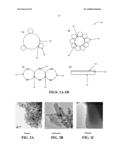
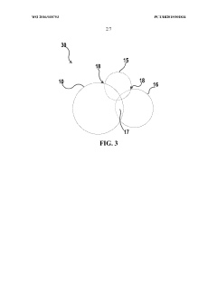
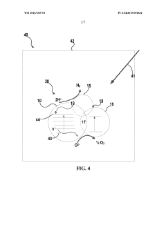
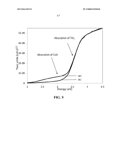
Photocatalytic hydrogen production from water over catalysts having p-n juncations and plasmonic materials
PatentWO2016030753A1
Innovation
- A photocatalyst combining a p-n junction formed by an n-type semiconductor material, such as titanium dioxide, with a p-type semiconductor and metal or metal alloy having surface plasmon resonance properties, which increases charge carrier lifetime and reduces recombination, allowing for efficient hydrogen and oxygen production without external bias or voltage.
Semiconductor device and method
PatentActiveUS20100230720A1
Innovation
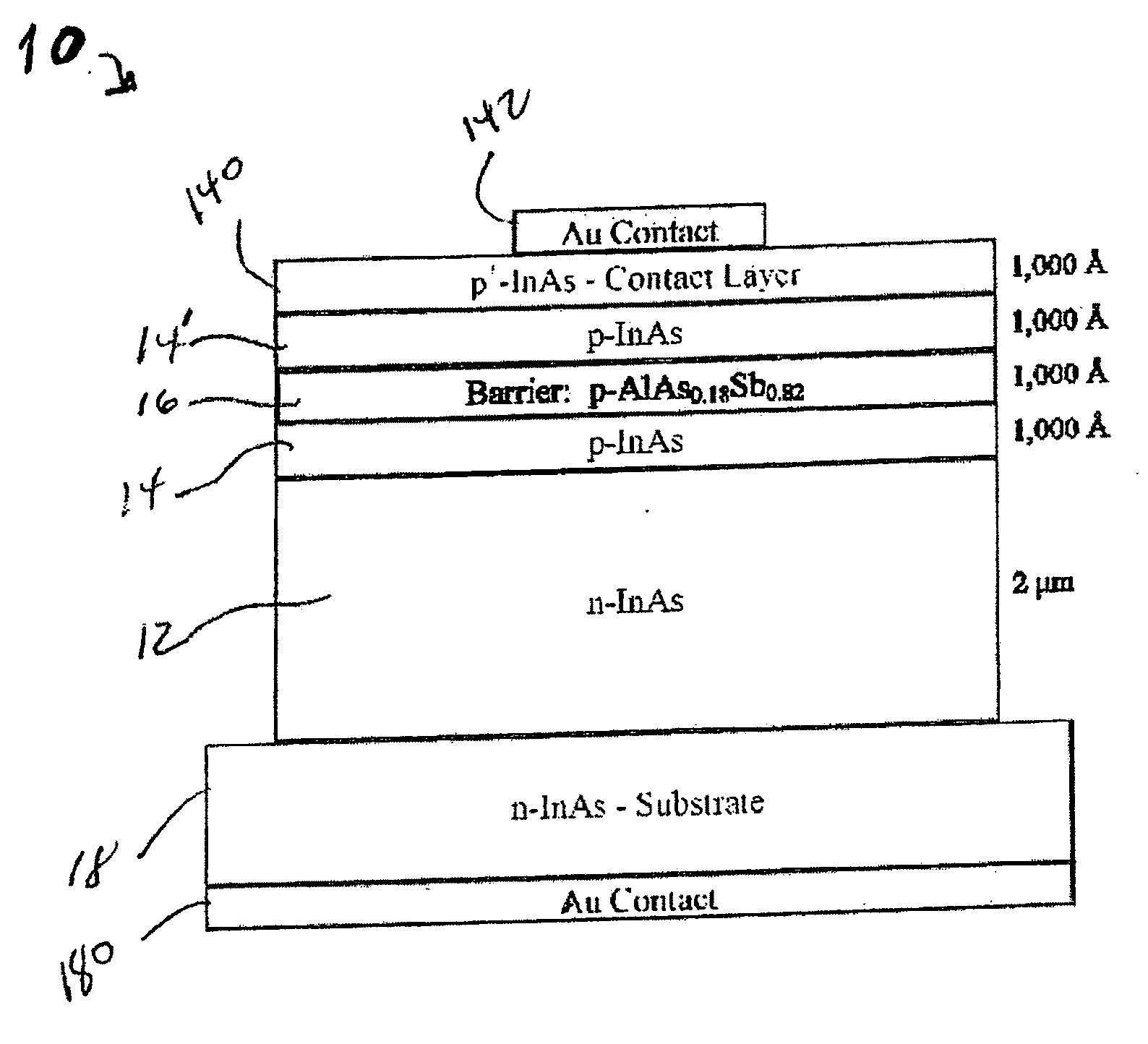
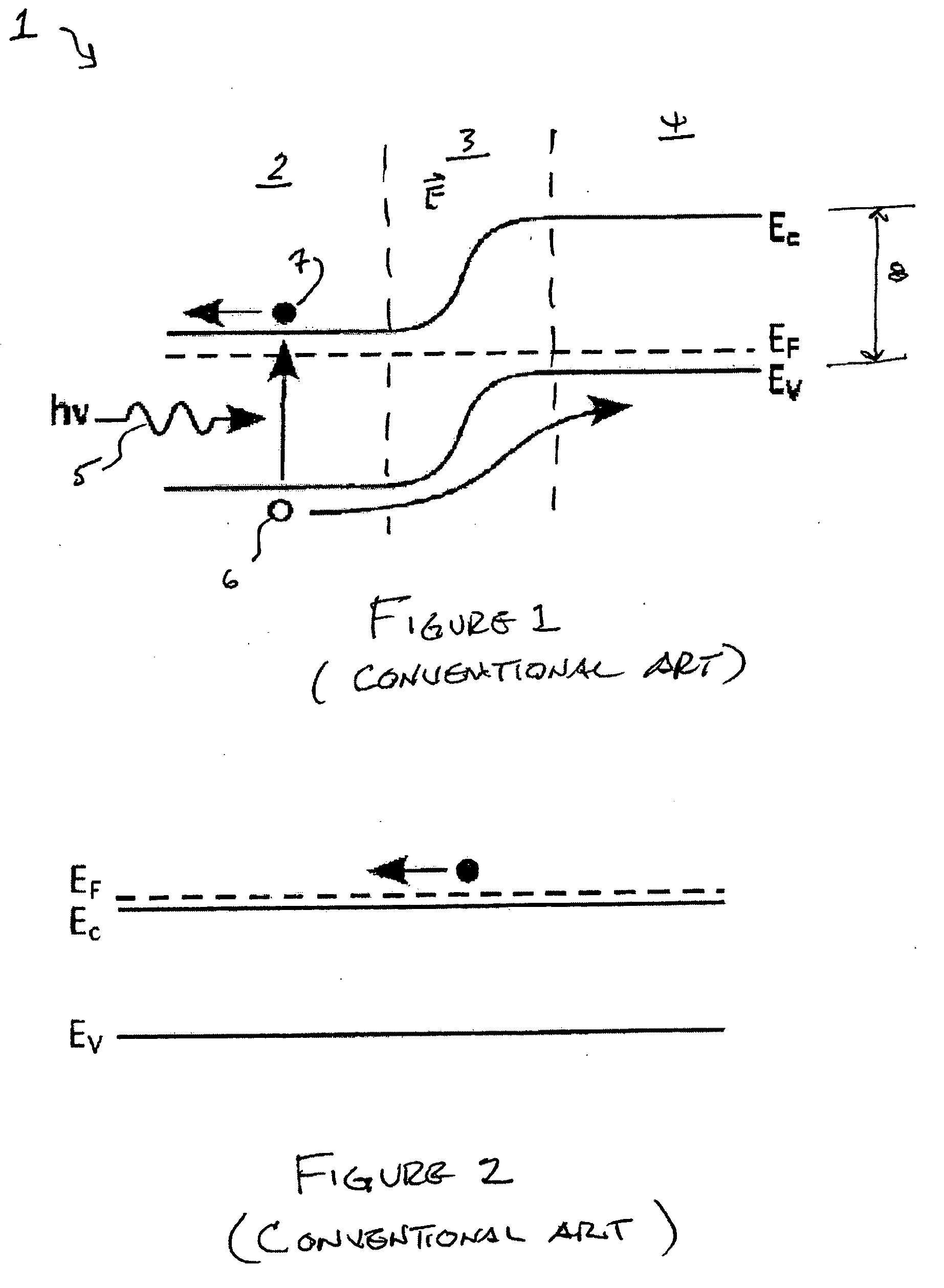
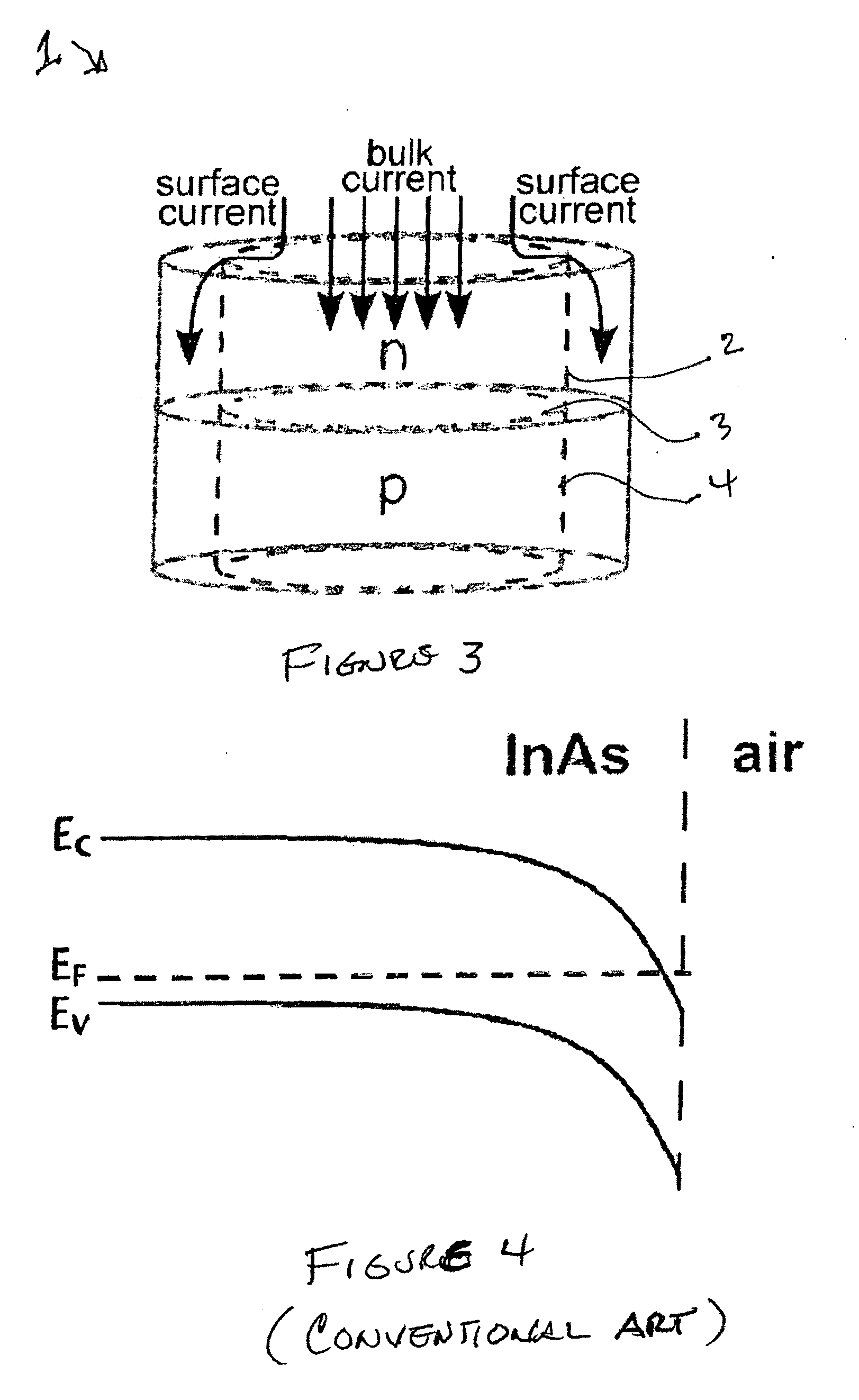
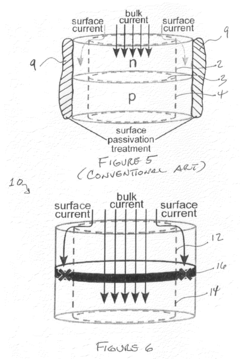
- The integration of unipolar barriers within the epitaxial structure of semiconductor devices during manufacturing, which blocks surface leakage currents while allowing bulk photocurrents to pass, eliminating the need for ex situ surface passivation treatments.
Manufacturing Processes and Cost Considerations
The manufacturing processes for different P-N junction types significantly impact both their performance characteristics and economic viability. Traditional homojunction manufacturing relies on well-established diffusion and ion implantation techniques, where dopants are introduced into silicon wafers through thermal processes. These methods benefit from decades of industrial refinement, resulting in highly optimized production lines with economies of scale that keep per-unit costs relatively low.
In contrast, heterojunction manufacturing requires more sophisticated epitaxial growth techniques such as molecular beam epitaxy (MBE) or metal-organic chemical vapor deposition (MOCVD). These processes demand ultra-high vacuum conditions and precise control of atomic layer deposition, substantially increasing both capital equipment costs and operational expenses. The complexity of creating atomically precise interfaces between different semiconductor materials adds another layer of manufacturing challenge.
Cost considerations extend beyond the fabrication process to material selection. Homojunctions typically utilize silicon, which remains abundant and cost-effective. Heterojunctions often incorporate more expensive compound semiconductors like gallium arsenide, indium phosphide, or gallium nitride, driving material costs higher. The price premium for these specialized materials can range from 3-10 times that of silicon, depending on purity requirements and market conditions.
Yield rates present another critical economic factor. Mature homojunction manufacturing processes consistently achieve yields exceeding 90% in high-volume production. Heterojunction fabrication, with its more complex material interfaces and stricter tolerance requirements, typically experiences lower yields, particularly during early production phases. This yield differential directly impacts per-unit costs and production scalability.
Equipment depreciation represents a substantial fixed cost component. Homojunction production equipment, while expensive, benefits from longer useful lifespans and established secondary markets. Heterojunction manufacturing equipment often faces faster technological obsolescence due to the rapidly evolving nature of compound semiconductor processing techniques.
Labor costs also differ significantly between junction types. Homojunction manufacturing has achieved higher levels of automation, reducing labor intensity. Heterojunction production frequently requires more specialized technical expertise and manual process monitoring, increasing labor costs per unit. This differential becomes particularly pronounced in regions with rising labor costs.
When evaluating output efficiency against manufacturing costs, heterojunctions generally deliver superior performance metrics but at substantially higher production costs. This cost-performance tradeoff creates distinct market segmentation, with heterojunctions dominating high-performance applications where cost sensitivity is lower, while homojunctions maintain advantage in cost-sensitive mass-market applications.
Environmental Impact and Sustainability Factors
The environmental impact of different P-N junction types represents a critical consideration in semiconductor technology selection, particularly as sustainability becomes increasingly important in technological development. Homojunction solar cells, while simpler to manufacture, typically require higher quantities of silicon and other semiconductor materials compared to heterojunction alternatives. This increased material consumption translates to greater resource extraction and associated environmental degradation.
Heterojunction designs, particularly those incorporating thin-film technologies, demonstrate significant advantages in material efficiency. These structures can achieve comparable or superior performance while utilizing substantially less semiconductor material—often up to 90% less than traditional homojunction designs. This reduction directly correlates with decreased mining activities and lower energy consumption during the manufacturing process.
Manufacturing processes between junction types also present notable environmental distinctions. Homojunction fabrication typically involves high-temperature diffusion processes that consume substantial energy. Conversely, heterojunction manufacturing often employs lower-temperature deposition techniques, reducing the carbon footprint of production facilities. Studies indicate that heterojunction manufacturing can reduce energy consumption by 30-40% compared to conventional homojunction processes.
Toxicity considerations vary significantly across junction technologies. While traditional silicon-based homojunctions present minimal toxicity concerns, certain high-efficiency heterojunction designs incorporate elements like cadmium, gallium, and indium that pose greater environmental risks during production, deployment, and end-of-life disposal. These materials require specialized handling protocols and recycling infrastructure to mitigate potential environmental contamination.
The operational lifespan of different junction technologies directly impacts their sustainability profile. Heterojunction designs typically demonstrate superior resistance to light-induced degradation, potentially extending operational lifetimes by 15-25% compared to homojunction alternatives. This longevity reduces replacement frequency and associated resource consumption over time.
End-of-life considerations reveal further distinctions. Simpler homojunction structures generally offer more straightforward recycling pathways, while complex heterojunction designs may require more sophisticated separation techniques to recover valuable or hazardous materials. Recent advances in circular economy approaches have improved recycling efficiencies for both junction types, though heterojunction recycling remains more resource-intensive.
Carbon payback periods—the time required for a solar technology to offset the emissions generated during its production—favor advanced heterojunction designs despite their more complex manufacturing. The superior efficiency and longevity of these junctions typically result in carbon payback periods 20-30% shorter than comparable homojunction technologies, enhancing their overall environmental value proposition.
Unlock deeper insights with Patsnap Eureka Quick Research — get a full tech report to explore trends and direct your research. Try now!
Generate Your Research Report Instantly with AI Agent
Supercharge your innovation with Patsnap Eureka AI Agent Platform!