P–N Junction in RF Devices: Signal Loss and Attenuation
SEP 5, 20259 MIN READ
Generate Your Research Report Instantly with AI Agent
Patsnap Eureka helps you evaluate technical feasibility & market potential.
RF P-N Junction Technology Background and Objectives
The P-N junction, a fundamental semiconductor structure, has been integral to electronic device development since its theoretical conception in the 1930s and practical implementation in the 1940s. This boundary between p-type and n-type semiconductors creates a depletion region that forms the basis for numerous electronic components. In radio frequency (RF) applications, P-N junctions serve critical functions in diodes, transistors, and integrated circuits that operate at frequencies ranging from megahertz to gigahertz.
The evolution of RF technology has consistently demanded improved performance from P-N junctions, particularly regarding signal integrity. Historical progression shows a clear trajectory from basic germanium diodes to advanced silicon and compound semiconductor implementations, with each generation addressing limitations of its predecessors. Contemporary RF systems for telecommunications, radar, and wireless networking require increasingly efficient components that minimize signal degradation.
Signal loss and attenuation in RF P-N junctions represent significant challenges that limit device performance. These phenomena occur through multiple mechanisms: resistive losses in semiconductor materials, capacitive effects at junction interfaces, carrier recombination dynamics, and parasitic impedances. As operating frequencies increase, these effects become more pronounced, creating bottlenecks in system performance.
The technical objectives for advancing P-N junction technology in RF applications focus on several key areas. Primary goals include reducing junction capacitance to improve high-frequency response, minimizing series resistance to decrease insertion loss, and optimizing doping profiles to control carrier dynamics. Additionally, researchers aim to develop novel junction architectures that can maintain performance integrity across broader frequency ranges and under varying power conditions.
Recent technological trends indicate growing interest in heterojunction structures, nanoscale junction engineering, and integration with emerging materials like wide-bandgap semiconductors. These approaches offer promising pathways to overcome traditional limitations. The convergence of advanced fabrication techniques, computational modeling, and materials science has accelerated innovation in this domain.
The strategic importance of addressing P-N junction signal loss extends beyond component-level improvements. Enhanced junction performance enables system-level advances in communication range, data throughput, energy efficiency, and miniaturization. As wireless technologies continue to proliferate across consumer, industrial, and defense sectors, the demand for optimized RF P-N junctions will intensify, driving further research and development in this critical technology area.
Market Analysis for Low-Loss RF Semiconductor Devices
The RF semiconductor device market is experiencing robust growth, driven by the proliferation of wireless communication technologies and the imminent rollout of 5G networks globally. Current market valuations indicate that the RF semiconductor segment reached approximately $17.8 billion in 2022, with projections suggesting a compound annual growth rate (CAGR) of 8.4% through 2028. This growth trajectory is particularly significant for low-loss RF semiconductor devices, which are becoming increasingly critical as higher frequencies are utilized in modern communication systems.
Consumer electronics, particularly smartphones and tablets, represent the largest application segment for low-loss RF devices, accounting for roughly 45% of the total market share. The telecommunications infrastructure sector follows closely, comprising about 30% of market demand, with the remainder distributed across automotive, aerospace, defense, and industrial applications.
The demand for low-loss RF semiconductor devices is primarily fueled by the need for improved signal integrity, reduced power consumption, and enhanced overall system efficiency. As wireless networks transition to higher frequency bands (mmWave) for 5G and future 6G implementations, the challenges associated with signal loss and attenuation at P-N junctions become more pronounced, creating a substantial market opportunity for innovative solutions.
Regional analysis reveals that Asia-Pacific dominates the market with approximately 40% share, led by manufacturing powerhouses like Taiwan, South Korea, and China. North America follows with 30% market share, driven by significant R&D investments and the presence of leading semiconductor companies. Europe accounts for 20% of the market, with the remaining 10% distributed across other regions.
Customer requirements are evolving rapidly, with increasing emphasis on devices that can operate efficiently at frequencies above 24 GHz while maintaining thermal stability and reliability. Market surveys indicate that system designers are willing to pay premium prices (typically 15-25% higher) for components that demonstrate superior performance in reducing signal loss at P-N junctions.
The competitive landscape is characterized by both established semiconductor manufacturers and emerging specialized firms focusing exclusively on RF optimization technologies. Recent market consolidation through mergers and acquisitions suggests that companies are strategically positioning themselves to capture larger shares of this growing segment.
Market forecasts indicate that the demand for low-loss RF semiconductor devices will continue to accelerate, with particular growth in applications requiring millimeter-wave frequencies, such as automotive radar systems, satellite communications, and next-generation wireless infrastructure. This presents significant opportunities for technological innovation addressing the fundamental challenges of P-N junction signal loss and attenuation.
Current Challenges in P-N Junction Signal Attenuation
P-N junctions in RF devices face significant challenges related to signal loss and attenuation, which limit their performance in high-frequency applications. The primary challenge stems from the inherent capacitance that forms at the junction interface. This junction capacitance creates a low-impedance path for RF signals, resulting in signal leakage and power loss, particularly as frequencies increase beyond several GHz. The depletion region, while necessary for device operation, acts as a dielectric barrier that stores energy rather than allowing efficient signal propagation.
Temperature dependence presents another critical challenge. As RF devices heat up during operation, the carrier concentration and mobility within the P-N junction change significantly. This thermal sensitivity causes variations in junction resistance and capacitance, leading to inconsistent signal attenuation characteristics across different operating conditions. For applications requiring stable performance across wide temperature ranges, this poses a substantial design constraint.
Carrier transit time limitations further exacerbate signal attenuation issues. At high frequencies, carriers cannot respond quickly enough to the rapidly changing electric fields, creating a phase lag between the input and output signals. This phenomenon, known as carrier injection delay, becomes particularly problematic in the gigahertz range where it manifests as increased insertion loss and distortion in the frequency response curve.
Material interface quality remains a persistent challenge. Even minor imperfections at the P-N junction boundary can create trap states that capture and release carriers unpredictably. These trapping mechanisms introduce noise and signal distortion, particularly affecting the linearity of RF amplifiers and the sensitivity of RF detectors. Advanced fabrication techniques have improved interface quality, but complete elimination of these defects remains elusive.
Parasitic elements surrounding the P-N junction compound the attenuation problems. Series resistance in the semiconductor bulk material, contact resistance at metal-semiconductor interfaces, and package inductance all contribute to the overall signal loss budget. These parasitic components form complex impedance networks that are difficult to model accurately, especially as device dimensions shrink to accommodate higher operating frequencies.
Radiation effects pose challenges for P-N junctions in aerospace and military RF applications. Exposure to ionizing radiation creates additional charge carriers and defects within the semiconductor material, altering the junction's electrical characteristics. This radiation-induced degradation accelerates signal attenuation and can permanently damage the device structure, necessitating radiation-hardened designs for critical applications.
Scaling limitations have emerged as devices continue to miniaturize. As P-N junctions shrink to nanometer dimensions, quantum effects begin to dominate device behavior, introducing new loss mechanisms not present in larger structures. Electron tunneling across ultra-thin depletion regions and increased surface-to-volume ratios contribute to signal attenuation through mechanisms that traditional semiconductor physics models struggle to accurately predict.
Contemporary Solutions for Minimizing RF Signal Loss
01 Signal attenuation measurement in P-N junctions
Various methods and devices are used to measure signal attenuation in P-N junctions. These techniques help in quantifying the loss of signal strength as it passes through semiconductor materials. Advanced measurement systems can detect minute changes in signal properties, allowing for precise characterization of junction behavior under different operating conditions. These measurements are crucial for optimizing device performance and understanding fundamental semiconductor physics.- Signal loss measurement in P-N junction devices: Various methods and systems are used to measure signal loss in P-N junction devices. These techniques involve analyzing the attenuation characteristics of signals passing through semiconductor junctions. Advanced measurement tools can quantify the degradation of signal strength across P-N junctions under different operating conditions, providing critical data for device optimization and performance evaluation.
- Optical signal attenuation in semiconductor junctions: P-N junctions in optical semiconductor devices experience signal attenuation that affects light transmission. This attenuation occurs due to absorption, scattering, and reflection at the junction interface. Understanding and mitigating these optical signal losses is crucial for applications in fiber optics, photonics, and optoelectronic devices where signal integrity across semiconductor junctions is essential.
- Temperature effects on P-N junction signal transmission: Temperature variations significantly impact signal attenuation in P-N junctions. As temperature increases, carrier mobility decreases and resistance increases, leading to greater signal loss. Thermal effects can alter the junction characteristics, affecting bandwidth and signal integrity. Compensation techniques and temperature-stable designs are implemented to maintain consistent signal transmission across varying thermal conditions.
- Frequency-dependent attenuation in semiconductor junctions: P-N junctions exhibit frequency-dependent signal attenuation characteristics where higher frequency signals typically experience greater loss. This phenomenon results from junction capacitance, carrier transit time limitations, and skin effect at higher frequencies. Understanding these frequency-dependent behaviors is essential for designing high-speed semiconductor devices and communication systems that maintain signal integrity across broad frequency ranges.
- Compensation techniques for P-N junction signal loss: Various compensation techniques are employed to mitigate signal loss in P-N junction devices. These include adaptive biasing, signal amplification, impedance matching, and specialized junction geometries. Advanced circuit designs incorporate feedback mechanisms to dynamically adjust for attenuation under varying conditions. These approaches help maintain signal integrity and improve the overall performance of semiconductor devices in telecommunications, sensing, and computing applications.
02 Optical signal processing in P-N junction devices
P-N junctions are utilized in optical signal processing applications where they convert, modulate, or detect light signals. Signal loss and attenuation in these optical applications occur due to absorption, reflection, and scattering mechanisms within the junction. Various designs and materials are employed to minimize these losses and enhance the efficiency of optical signal transmission through semiconductor interfaces.Expand Specific Solutions03 Temperature effects on P-N junction signal attenuation
Temperature variations significantly impact signal attenuation in P-N junctions by affecting carrier mobility, junction resistance, and recombination rates. As temperature increases, thermal noise typically increases while carrier mobility decreases, leading to greater signal attenuation. Compensation techniques and temperature-stable designs are implemented to maintain consistent signal quality across varying thermal conditions in semiconductor devices.Expand Specific Solutions04 Wireless communication signal processing with P-N junctions
P-N junctions play a critical role in wireless communication systems where they are used in signal detection, amplification, and processing circuits. Signal attenuation occurs during these processes due to junction capacitance, resistance, and other parasitic effects. Advanced designs minimize these losses through optimized doping profiles, junction geometries, and circuit configurations to maintain signal integrity in wireless applications.Expand Specific Solutions05 Computational modeling of signal loss in P-N junctions
Computational models and simulation techniques are developed to predict and analyze signal loss mechanisms in P-N junctions. These models incorporate physical parameters such as doping concentrations, junction geometry, material properties, and operating conditions to simulate signal propagation and attenuation. Advanced algorithms and software tools enable designers to optimize junction characteristics before physical implementation, reducing development time and improving performance.Expand Specific Solutions
Leading RF Semiconductor Manufacturers and Research Institutions
The RF device market, particularly focusing on P-N junction signal loss and attenuation challenges, is in a mature growth phase with increasing demand driven by 5G deployment and IoT expansion. The global market is projected to reach significant scale as telecommunications infrastructure continues to evolve. Leading semiconductor manufacturers like Taiwan Semiconductor, Infineon Technologies, and Qualcomm have developed advanced solutions to minimize signal degradation in RF applications. Research institutions including Xidian University and University of Southampton are contributing breakthrough innovations in junction optimization. Companies such as Huawei and Ericsson are implementing these technologies in commercial telecommunications equipment, while specialized firms like EXFO provide testing solutions to measure and validate RF performance metrics.
Infineon Technologies AG
Technical Solution: Infineon has developed advanced Silicon Carbide (SiC) and Gallium Nitride (GaN) based RF devices that minimize P-N junction losses through innovative junction engineering. Their CoolSiC™ and CoolGaN™ technologies incorporate optimized doping profiles and reduced junction capacitance to minimize signal attenuation at high frequencies. Infineon's approach includes specialized buffer layers between P and N regions to reduce parasitic effects and improve linearity. Their RF power transistors feature proprietary junction termination extension (JTE) structures that reduce electric field crowding at junction edges, significantly decreasing leakage currents that contribute to signal loss. Additionally, Infineon has implemented advanced thermal management solutions integrated directly at the junction level to maintain optimal performance under high-power RF conditions, as thermal variations can exacerbate junction-related losses.
Strengths: Industry-leading SiC and GaN technology with superior high-frequency performance and reduced junction capacitance. Comprehensive device portfolio spanning multiple power and frequency ranges. Weaknesses: Higher manufacturing costs compared to silicon-based alternatives, and some devices require specialized packaging to fully realize performance benefits.
Taiwan Semiconductor Manufacturing Co., Ltd.
Technical Solution: TSMC has developed specialized RF-optimized semiconductor processes that address P-N junction signal loss through advanced material engineering and junction design. Their RF-CMOS technology features ultra-shallow junctions with precisely controlled doping profiles to minimize junction capacitance and series resistance. TSMC's RF SOI (Silicon-on-Insulator) process incorporates a buried oxide layer that effectively isolates P-N junctions from the substrate, significantly reducing parasitic capacitance and substrate coupling losses that typically degrade RF performance. Their advanced SiGe BiCMOS technology utilizes graded germanium profiles in the base region of bipolar transistors to optimize the emitter-base and collector-base junctions for enhanced RF performance. TSMC has also pioneered specialized silicide and contact technologies that reduce junction access resistance, a critical factor in minimizing signal attenuation in RF devices. Additionally, their wafer-level packaging solutions provide shorter interconnect paths that preserve signal integrity by minimizing transmission line effects between junctions.
Strengths: Industry-leading semiconductor fabrication capabilities with specialized RF-optimized processes. Extensive experience in high-volume manufacturing of RF components with consistent performance. Weaknesses: As a foundry, TSMC depends on customers' designs, limiting their direct influence on final device architecture. Some advanced processes have higher costs that may be prohibitive for certain applications.
Key Patents and Research on P-N Junction Loss Reduction
P-N Junction for Use as an RF Mixer from GHZ to THZ Frequencies
PatentInactiveUS20090302352A1
Innovation
- The use of narrow bandgap semiconductors in p-n heterojunction diodes allows for lower local oscillator power operation without a DC bias, utilizing molecular beam epitaxy to grow thin layers with high electron mobilities and low parasitic resistances, enabling operation at higher frequencies.
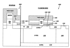
Vertical p-n junction device and method of forming same
PatentInactiveUS20080258173A1
Innovation
- A P-N junction device with a raised polycrystalline silicon germanium (SiGe) anode is formed, where the cathode contact is positioned within the same shallow trench isolation (STI) opening as the anode, reducing parasitic resistance and capacitance, and the cathode implant area is minimized.
Thermal Management Strategies for RF P-N Junctions
Thermal management is a critical aspect of RF P-N junction performance, as excessive heat generation can significantly impact signal integrity through increased attenuation and loss. The thermal challenges in RF P-N junctions primarily stem from the inherent resistance at the junction interface, where carrier recombination and lattice scattering generate heat during high-frequency operation.
Conventional cooling approaches for RF P-N junctions include passive heat sinking, where thermally conductive materials like copper or aluminum are attached directly to the semiconductor substrate. These materials provide pathways for heat dissipation through conduction. However, the thermal boundary resistance between different materials often creates bottlenecks in the heat flow path, limiting cooling efficiency.
Advanced thermal interface materials (TIMs) have emerged as a solution to reduce contact resistance between the junction and heat sink. Graphene-based TIMs demonstrate superior thermal conductivity (up to 5000 W/m·K) compared to traditional materials, enabling more efficient heat transfer away from the junction region. Metal matrix composites incorporating diamond particles have also shown promise, offering thermal conductivities exceeding 600 W/m·K while maintaining electrical isolation properties.
Active cooling strategies represent another approach for high-power RF applications. Microchannel liquid cooling systems integrated directly into semiconductor packages can achieve heat flux dissipation exceeding 500 W/cm². These systems utilize microfluidic channels etched into the substrate to circulate coolants in close proximity to the junction, significantly reducing thermal resistance.
Thermoelectric cooling (TEC) modules based on the Peltier effect provide precise temperature control for RF P-N junctions. By applying current across semiconductor junctions, these modules can pump heat away from sensitive areas, maintaining optimal operating temperatures. Recent advances in bismuth telluride-based TECs have improved cooling efficiency by up to 30% compared to previous generations.
Phase-change materials (PCMs) offer passive thermal management through latent heat absorption. When integrated into RF device packaging, PCMs can absorb thermal energy during peak operation periods and release it during idle times, effectively dampening temperature fluctuations. This approach is particularly valuable for pulsed RF applications where thermal cycling can accelerate device degradation.
Thermal simulation and modeling tools have become essential for optimizing junction thermal management. Finite element analysis and computational fluid dynamics enable designers to predict hotspot formation and optimize cooling strategies before physical prototyping. These tools have reduced thermal design iterations by approximately 40%, accelerating development cycles for RF devices with complex P-N junction structures.
Materials Science Advancements for Enhanced RF Performance
Recent advancements in materials science have revolutionized the performance capabilities of RF devices, particularly in addressing the critical challenges of signal loss and attenuation in P-N junctions. The development of novel semiconductor materials with enhanced carrier mobility and reduced parasitic capacitance has significantly improved RF signal integrity across junction interfaces.
Wide-bandgap semiconductors such as Gallium Nitride (GaN) and Silicon Carbide (SiC) have emerged as superior alternatives to traditional silicon in high-frequency applications. These materials demonstrate exceptional electron mobility—GaN offering up to 2000 cm²/V·s compared to silicon's 1400 cm²/V·s—while maintaining stability at higher operating temperatures and power densities. This translates directly to reduced signal attenuation in P-N junctions operating at RF frequencies.
Engineered substrate technologies have further enhanced RF performance through strategic manipulation of crystal lattice structures. Techniques such as strain engineering and epitaxial growth processes have enabled the creation of heterojunction interfaces with minimized lattice mismatch, reducing scattering effects that contribute to signal degradation. Silicon-on-insulator (SOI) and silicon-on-sapphire (SOS) substrates have demonstrated up to 30% reduction in junction capacitance compared to bulk silicon implementations.
Nanoscale material innovations have introduced quantum well and quantum dot structures that fundamentally alter carrier behavior at junction interfaces. These structures create precisely controlled energy bandgaps that optimize carrier transport across the depletion region, resulting in measurably improved RF signal transmission. Recent research has demonstrated quantum well P-N junctions achieving Q-factors exceeding 200 at frequencies above 10 GHz.
Surface passivation techniques utilizing advanced dielectric materials have addressed interface state issues that traditionally plague RF performance. Atomic layer deposition (ALD) of high-k dielectrics has enabled the creation of nearly defect-free interfaces, reducing surface recombination velocities by orders of magnitude. This advancement has been particularly impactful in minimizing parasitic effects that contribute to signal attenuation at higher frequencies.
Composite semiconductor materials, including III-V compounds like InGaAs and InP, have demonstrated exceptional RF characteristics with electron mobilities exceeding 10,000 cm²/V·s. These materials enable the fabrication of P-N junctions with dramatically reduced resistance-capacitance (RC) time constants, allowing for operation at frequencies approaching the terahertz range while maintaining signal integrity across the junction.
Unlock deeper insights with Patsnap Eureka Quick Research — get a full tech report to explore trends and direct your research. Try now!
Generate Your Research Report Instantly with AI Agent
Supercharge your innovation with Patsnap Eureka AI Agent Platform!