P–N Junction Design: Impact On Energy Loss Minimization
SEP 4, 202510 MIN READ
Generate Your Research Report Instantly with AI Agent
Patsnap Eureka helps you evaluate technical feasibility & market potential.
P-N Junction Evolution and Energy Efficiency Goals
The P-N junction, a fundamental semiconductor structure, has undergone significant evolution since its theoretical conception by Alan Wilson in 1939 and practical demonstration by Russell Ohl at Bell Labs in 1940. This interface between p-type and n-type semiconductors has become the cornerstone of modern electronics, enabling the functionality of diodes, transistors, solar cells, and numerous other electronic devices. The historical trajectory of P-N junction development reveals a consistent focus on improving efficiency and reducing energy losses.
Early P-N junctions suffered from substantial energy losses due to recombination processes, parasitic resistances, and thermal inefficiencies. The progression from germanium to silicon-based junctions in the 1950s marked the first major advancement in energy efficiency. Silicon offered better thermal stability and lower leakage currents, significantly reducing energy dissipation in electronic devices.
The 1970s and 1980s witnessed the introduction of compound semiconductors like gallium arsenide (GaAs) and indium phosphide (InP), which provided higher electron mobility and improved energy conversion efficiency. These materials enabled the development of more efficient solar cells and high-frequency devices with reduced energy losses.
The miniaturization trend following Moore's Law has continuously pushed P-N junction designs toward nanoscale dimensions, necessitating novel approaches to combat quantum tunneling effects and increased leakage currents that contribute to energy losses. Advanced junction engineering techniques such as graded junctions, heterojunctions, and quantum well structures have emerged to address these challenges.
Current technical goals in P-N junction design center around achieving theoretical efficiency limits while minimizing energy losses. For power electronics applications, wide-bandgap semiconductors like silicon carbide (SiC) and gallium nitride (GaN) are being extensively researched to reduce switching losses and enable higher operating temperatures and voltages.
In photovoltaic applications, the goal is to approach the Shockley-Queisser limit of solar energy conversion efficiency while minimizing recombination losses. Multi-junction designs, quantum dot structures, and perovskite materials represent promising pathways toward this objective.
For integrated circuits, the focus has shifted to reducing static and dynamic power consumption through improved junction designs that minimize leakage currents and switching losses. Three-dimensional integration and novel channel materials like graphene and transition metal dichalcogenides are being explored to overcome silicon's inherent limitations.
The overarching technical objective remains consistent: to design P-N junctions that approach ideal behavior with minimal energy dissipation, thereby enabling more efficient electronic systems across all application domains from consumer electronics to renewable energy technologies.
Market Demand for Low-Loss Semiconductor Devices
The semiconductor industry is witnessing an unprecedented demand for low-loss semiconductor devices, driven primarily by the global push for energy efficiency and sustainable technology solutions. This market demand spans multiple sectors including consumer electronics, automotive, industrial automation, renewable energy, and telecommunications, with each sector requiring specialized semiconductor solutions that minimize energy losses.
Power electronics applications represent one of the largest market segments demanding improved P-N junction designs with minimized energy losses. The global power semiconductor market, which heavily relies on efficient P-N junctions, continues to expand rapidly as industries transition toward electrification. Electric vehicles (EVs) and hybrid electric vehicles (HEVs) particularly require high-efficiency power semiconductors to maximize battery life and driving range, creating substantial market pull for advanced low-loss semiconductor technologies.
Data centers and cloud computing infrastructure constitute another significant market driver. With the exponential growth in data processing requirements, energy consumption in data centers has become both an environmental concern and a major operational cost. Low-loss semiconductor devices can dramatically reduce power consumption, heat generation, and cooling requirements, offering substantial operational cost savings while supporting sustainability goals.
The renewable energy sector presents perhaps the most compelling case for low-loss semiconductor advancement. Solar inverters, wind power converters, and energy storage systems all rely heavily on semiconductor efficiency to maximize energy harvest and minimize conversion losses. As renewable energy adoption accelerates globally, the demand for higher-efficiency semiconductor devices grows proportionally, creating a virtuous cycle of innovation and implementation.
Consumer electronics manufacturers are increasingly prioritizing energy efficiency as a key product differentiator. Extended battery life in portable devices, reduced heat generation in compact designs, and lower power consumption in always-on devices all depend on semiconductor efficiency improvements. This market segment drives high-volume adoption of advanced semiconductor technologies, creating economies of scale that benefit the entire industry.
The telecommunications industry, particularly with the ongoing 5G infrastructure deployment, represents another significant market for low-loss semiconductors. Base stations and network equipment operate continuously, making energy efficiency a critical factor in operational costs and environmental impact. The higher frequencies and power densities of 5G systems further amplify the importance of minimizing energy losses in semiconductor components.
Industrial automation and the Industrial Internet of Things (IIoT) are creating new applications for low-loss semiconductors in factory automation, process control, and smart manufacturing. These applications often operate in challenging environments where heat dissipation is problematic, making energy efficiency not just an economic consideration but a fundamental design requirement.
Current P-N Junction Technology Limitations
Despite significant advancements in semiconductor technology, current P-N junction designs face several critical limitations that contribute to energy losses in electronic devices. The conventional P-N junction structure, while fundamental to semiconductor operation, exhibits inherent inefficiencies that become increasingly problematic as devices scale down and power requirements become more stringent.
Recombination losses represent one of the most significant challenges in current P-N junction technology. Both bulk recombination within the semiconductor material and surface recombination at interfaces result in energy dissipation through heat rather than useful electrical output. These losses are particularly pronounced in high-power applications and can account for efficiency reductions of 10-15% in typical power conversion systems.
Parasitic resistances present another major limitation. Series resistance in the semiconductor bulk, contact resistance at metal-semiconductor interfaces, and sheet resistance in the diffused regions all contribute to I²R losses. As current densities increase in modern applications, these resistive components become increasingly significant bottlenecks to efficiency.
Junction capacitance effects create switching losses that become particularly problematic in high-frequency applications. The depletion capacitance and diffusion capacitance inherent to P-N junctions limit switching speeds and create energy dissipation during state transitions. This limitation has become more pronounced as applications demand faster switching frequencies to reduce passive component sizes.
Temperature sensitivity remains a persistent challenge, with junction performance degrading significantly at elevated temperatures. The temperature coefficient of P-N junctions leads to increased leakage currents and reduced breakdown voltages as temperatures rise, creating a negative feedback loop where losses generate heat that further increases losses.
Manufacturing variability introduces additional inefficiencies through non-uniform doping profiles and junction depths. Current fabrication techniques struggle to maintain perfect consistency across large wafers, resulting in performance variations that necessitate conservative design approaches that sacrifice optimal efficiency.
Edge termination effects at junction peripheries create localized high-field regions that can lead to premature breakdown and increased leakage currents. These effects become more pronounced as device geometries shrink, limiting the practical voltage ratings and safe operating areas of P-N junction devices.
The fundamental bandgap limitations of silicon, the predominant semiconductor material, impose theoretical efficiency limits that conventional P-N junction designs are approaching. While wide-bandgap materials offer potential improvements, their integration with existing silicon-based technology presents significant technical and economic challenges.
Contemporary P-N Junction Energy Loss Reduction Methods
01 Energy loss reduction in semiconductor devices
Various techniques are employed to reduce energy losses in p-n junction semiconductor devices. These include optimizing the junction structure, improving carrier mobility, and enhancing the electrical characteristics of the junction interface. By minimizing resistance and recombination losses at the junction, overall device efficiency can be significantly improved, leading to better performance in applications such as solar cells and power electronics.- Energy loss reduction in semiconductor devices: Various techniques are employed to reduce energy losses in p-n junction semiconductor devices. These include optimizing the junction structure, improving carrier mobility, and reducing parasitic resistances. By carefully designing the doping profiles and junction geometries, the energy dissipation during carrier transport across the junction can be minimized, leading to more efficient device operation and reduced heat generation.
- Thermal management of p-n junctions: Thermal management strategies are crucial for controlling energy losses in p-n junctions. These include heat dissipation structures, thermal interface materials, and cooling systems designed to remove excess heat generated during operation. Effective thermal management prevents performance degradation, increases device reliability, and extends operational lifetime by maintaining optimal junction temperatures and reducing thermally-induced energy losses.
- Measurement and analysis of p-n junction energy losses: Advanced measurement techniques and analytical methods are used to quantify and characterize energy losses in p-n junctions. These include electrical characterization, thermal imaging, and computational modeling approaches that help identify loss mechanisms and their relative contributions. By accurately measuring and analyzing energy losses, engineers can develop more targeted optimization strategies for improving device efficiency.
- Novel materials and structures for reducing junction losses: Innovative materials and junction structures are being developed to minimize energy losses in semiconductor devices. These include wide bandgap semiconductors, heterojunction designs, and nanostructured materials that offer superior electrical properties. By incorporating these advanced materials and structures, significant reductions in junction resistance, recombination losses, and parasitic effects can be achieved, leading to higher overall energy efficiency.
- Energy harvesting from p-n junction losses: Novel approaches are being developed to recover and utilize energy that would otherwise be lost in p-n junctions. These include thermoelectric recovery systems, photonic recycling mechanisms, and integrated energy storage solutions. By capturing and repurposing energy that would typically be dissipated as heat, these technologies improve the overall system efficiency and sustainability of semiconductor devices and circuits.
02 Thermal management of p-n junctions
Thermal management techniques are crucial for controlling energy losses in p-n junctions. These approaches focus on heat dissipation methods, temperature monitoring systems, and materials with improved thermal conductivity. Effective thermal management prevents performance degradation due to excessive heat generation at the junction, which can lead to increased resistance and energy losses through phonon scattering and other thermal mechanisms.Expand Specific Solutions03 Optical and photonic applications of p-n junctions
P-n junctions are widely used in optical and photonic applications where energy loss management is critical. These applications include photodetectors, light-emitting diodes, and optical sensors. Specialized junction designs minimize energy losses during photon-electron conversion processes, improving quantum efficiency and reducing heat generation. Advanced materials and novel junction geometries help optimize the optical performance while minimizing unwanted energy dissipation.Expand Specific Solutions04 Power electronics and high-frequency applications
In power electronics and high-frequency applications, p-n junction energy losses significantly impact overall system efficiency. Specialized junction designs focus on reducing switching losses, reverse recovery losses, and conduction losses. Advanced semiconductor materials and novel device architectures help minimize these energy losses, enabling more efficient power conversion and high-frequency operation in applications ranging from power supplies to wireless communication systems.Expand Specific Solutions05 Novel materials and fabrication techniques
Innovative materials and fabrication techniques are being developed to minimize energy losses in p-n junctions. These include wide-bandgap semiconductors, heterojunction structures, and advanced doping profiles. New manufacturing processes enable more precise control over junction properties, resulting in reduced defect density and improved carrier transport. These advancements lead to p-n junctions with significantly lower energy losses across various applications.Expand Specific Solutions
Leading Semiconductor Manufacturers and Research Institutions
The P-N junction design for energy loss minimization is currently in a growth phase, with increasing market demand driven by energy efficiency requirements across multiple sectors. The global market is expanding rapidly, projected to reach significant scale as power electronics applications proliferate in renewable energy, electric vehicles, and industrial systems. Technologically, the field shows varying maturity levels among key players. Leading companies like Toshiba, MACOM, and Samsung Electronics have established advanced capabilities in junction optimization, while research institutions including University of Electronic Science & Technology of China and Xi'an Jiaotong University are pioneering next-generation designs. Semiconductor specialists such as MaxPower, Renesas, and GlobalFoundries are developing proprietary junction architectures that demonstrate promising energy loss reductions, indicating a competitive landscape where both established manufacturers and specialized innovators are driving technological advancement.
Toshiba Corp.
Technical Solution: Toshiba has pioneered super-junction technology for power MOSFETs that fundamentally reimagines P-N junction design for energy loss minimization. Their approach creates alternating P and N pillars that extend vertically through the drift region, allowing for higher doping concentrations while maintaining high breakdown voltage. This structure significantly reduces on-resistance per unit area compared to conventional planar junctions, with demonstrated improvements of over 50% in specific on-resistance. Toshiba's research has extended to curved P-N junction designs that distribute electric fields more uniformly, preventing localized field crowding that leads to premature breakdown and energy losses. They've implemented precise charge-balancing techniques that optimize the relationship between pillar doping concentrations, dimensions, and spacing to minimize conduction losses while maximizing blocking capability. Additionally, Toshiba has developed specialized junction termination structures that prevent peripheral breakdown effects, allowing their devices to operate closer to theoretical performance limits across a wide temperature range.
Strengths: Toshiba's super-junction technology provides exceptional performance in high-voltage applications where energy efficiency is critical. Their extensive experience in power semiconductor manufacturing enables reliable production of complex junction structures. Weaknesses: The complex fabrication process for their advanced junction designs requires more processing steps than conventional junctions, potentially increasing manufacturing costs and complexity.
MaxPower Semiconductor, Inc.
Technical Solution: MaxPower Semiconductor has developed innovative P-N junction designs specifically targeting energy loss minimization in power devices. Their proprietary XTREMOS technology implements a unique junction architecture that combines aspects of trench, planar, and super-junction concepts to create optimized electric field distributions. This approach allows for higher doping concentrations in conduction regions while maintaining blocking capability, resulting in significantly reduced on-resistance and corresponding conduction losses. MaxPower's research has demonstrated devices with specific on-resistance improvements of up to 60% compared to conventional junction designs at equivalent voltage ratings. Their technology incorporates specialized charge-balancing techniques that precisely control the relationship between P and N regions to minimize both static and dynamic losses. Additionally, MaxPower has developed advanced edge termination structures that prevent field crowding at junction peripheries, allowing their devices to operate closer to theoretical performance limits. Their junction designs also feature optimized geometries that reduce parasitic capacitances, minimizing switching losses in high-frequency applications.
Strengths: MaxPower's specialized focus on power semiconductor technology has resulted in junction designs specifically optimized for energy efficiency in switching applications. Their innovative approach combines multiple junction technologies to achieve performance beyond what's possible with any single conventional design. Weaknesses: As a smaller company, MaxPower may have more limited manufacturing capabilities compared to larger semiconductor manufacturers, potentially affecting their ability to scale production of their advanced junction designs.
Key Patents in P-N Junction Efficiency Enhancement
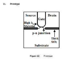
Minimization of leakage currents and reduction of area of mosfet structure for CMOS transistor circuits in the semiconductor industry
PatentPendingIN202331053801A
Innovation
- The proposed solution involves minimizing the junction area by inserting a silicon dioxide insulator between p and n regions, replacing gate oxide with high-k dielectric materials, and optimizing the transistor structure to reduce leakage currents, while maintaining or improving performance and reducing area and production costs.
Thermo-electric element
PatentInactiveEP2009709A2
Innovation
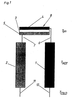
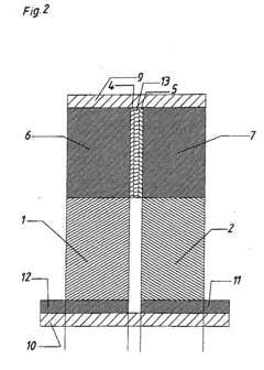
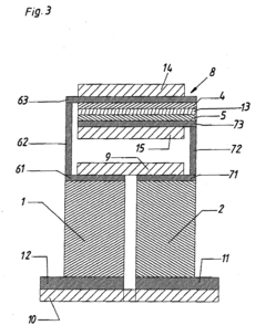
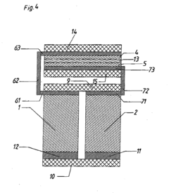
- Incorporating a pn junction as the generation center of electrons and holes within a thermocouple, where thermal excitation generates electron-hole pairs, allowing for independent optimization of charge carrier generation and transport, and using materials with lower band gaps to enhance power density and efficiency.
Materials Science Innovations for P-N Junction Performance
Recent advancements in materials science have revolutionized P-N junction design, offering unprecedented opportunities for energy loss minimization. Traditional silicon-based junctions are increasingly being enhanced or replaced by novel materials that exhibit superior electronic properties. Compound semiconductors such as gallium arsenide (GaAs), gallium nitride (GaN), and silicon carbide (SiC) demonstrate significantly reduced energy losses due to their wider bandgaps and higher electron mobility compared to conventional silicon.
Nanomaterials represent another frontier in P-N junction innovation. Quantum dots, nanowires, and two-dimensional materials like graphene and transition metal dichalcogenides (TMDs) enable precise control over electronic properties at the nanoscale. These materials facilitate the creation of ultra-thin junctions with minimal recombination losses and enhanced carrier transport efficiency, directly addressing energy dissipation challenges.
Perovskite materials have emerged as particularly promising candidates for next-generation P-N junctions. Their tunable bandgap, exceptional light absorption capabilities, and low-cost processing methods make them ideal for photovoltaic applications. Recent research has demonstrated perovskite-based junctions achieving theoretical efficiency limits with minimal energy losses, though stability concerns remain a focus of ongoing research.
Interface engineering has become a critical aspect of materials innovation for P-N junctions. Novel passivation techniques using atomic layer deposition (ALD) and selective surface treatments have significantly reduced interface recombination losses. Additionally, the development of gradient-composition interfaces has minimized band discontinuities that traditionally contribute to energy losses through carrier scattering and recombination.
Heterostructure designs incorporating multiple materials with complementary properties represent another significant advancement. These structures enable band engineering to optimize carrier flow and minimize thermalization losses. For instance, multi-junction designs with carefully selected materials can capture a broader spectrum of energy while maintaining high voltage output, crucial for applications ranging from solar cells to power electronics.
Doping innovations have also contributed substantially to energy loss reduction. Precision doping techniques, including delta doping and selective area doping, allow for unprecedented control over carrier concentration profiles. Advanced ion implantation methods and in-situ doping during epitaxial growth have enabled the creation of optimized junction profiles that minimize parasitic resistance while maintaining desired electronic characteristics.
Thermal Management Strategies in Semiconductor Devices
Thermal management in semiconductor devices has become increasingly critical as P-N junction designs evolve to minimize energy losses. The thermal behavior of these junctions directly impacts device efficiency, reliability, and overall performance. Conventional cooling methods such as heat sinks and fans are proving inadequate for modern high-power density applications where P-N junctions generate significant heat during operation.
Advanced thermal interface materials (TIMs) represent a significant advancement in managing junction temperature. These materials, including metal-based composites and phase-change materials, provide superior thermal conductivity between the junction and heat dissipation components. Recent developments in diamond-based TIMs have demonstrated thermal conductivity values exceeding 2000 W/m·K, dramatically reducing thermal resistance at P-N junction interfaces.
Microfluidic cooling technologies have emerged as particularly effective for P-N junction thermal management. These systems utilize microscale channels directly integrated into semiconductor substrates, allowing coolant to flow in close proximity to heat-generating junctions. Studies indicate that microfluidic cooling can reduce junction temperatures by up to 60% compared to conventional air cooling, significantly minimizing temperature-dependent energy losses.
Three-dimensional heat spreading techniques address the challenge of localized hotspots at P-N junctions. By incorporating vertical thermal vias and embedded heat pipes within the semiconductor structure, heat can be efficiently distributed throughout the device. This approach has proven especially valuable in power electronics where P-N junction temperature gradients can lead to premature device failure and increased energy dissipation.
Dynamic thermal management systems represent the cutting edge of junction cooling technology. These adaptive systems utilize temperature sensors and control algorithms to adjust cooling parameters in real-time based on junction operating conditions. Implementation of machine learning algorithms has enabled predictive thermal management, anticipating temperature spikes before they occur and adjusting cooling resources accordingly.
Integration of thermoelectric cooling elements directly at the P-N junction interface offers promising results for precise temperature control. These solid-state devices can actively pump heat away from critical junctions when supplied with electrical current. Recent breakthroughs in thin-film thermoelectric materials have improved cooling efficiency by over 40%, making this approach increasingly viable for energy loss minimization in high-performance semiconductor applications.
The development of thermally aware circuit design methodologies complements physical cooling solutions. By considering thermal behavior during the P-N junction design phase, engineers can optimize layout, doping profiles, and junction geometries to minimize heat generation. Simulation tools that accurately model electro-thermal coupling effects have become essential for predicting and mitigating energy losses in advanced semiconductor devices.
Unlock deeper insights with Patsnap Eureka Quick Research — get a full tech report to explore trends and direct your research. Try now!
Generate Your Research Report Instantly with AI Agent
Supercharge your innovation with Patsnap Eureka AI Agent Platform!