P–N Junction vs MOSFET: Speed and Energy Efficiency
SEP 4, 20259 MIN READ
Generate Your Research Report Instantly with AI Agent
Patsnap Eureka helps you evaluate technical feasibility & market potential.
P-N Junction and MOSFET Technology Evolution
The evolution of semiconductor technology has been marked by two pivotal innovations: the P-N junction and the Metal-Oxide-Semiconductor Field-Effect Transistor (MOSFET). The P-N junction, first theorized by Russell Ohl in 1939 and demonstrated in 1940, represents the foundational element of semiconductor devices, enabling the basic rectification properties that underpin diodes and transistors. This discovery laid the groundwork for the first transistor developed at Bell Labs in 1947, which utilized two P-N junctions to create a point-contact transistor.
The trajectory of P-N junction technology progressed through the 1950s with the development of the bipolar junction transistor (BJT), which improved upon earlier designs by offering better stability and manufacturability. However, these devices faced inherent limitations in terms of power consumption and integration density, which became increasingly problematic as electronics miniaturization accelerated.
The MOSFET emerged as a revolutionary solution in 1959 when Mohamed Atalla and Dawon Kahng at Bell Labs fabricated the first working device. Unlike BJTs, MOSFETs operate on the principle of field effect, controlling current flow through an electric field rather than through direct carrier injection. This fundamental difference enabled significant advantages in power efficiency and scalability.
The 1960s and 1970s witnessed the refinement of MOSFET technology, with key innovations including the development of complementary metal-oxide-semiconductor (CMOS) architecture by Frank Wanlass in 1963. CMOS technology, utilizing both n-type and p-type MOSFETs, dramatically reduced power consumption during standby operations, addressing one of the critical limitations of previous semiconductor technologies.
The 1980s marked the beginning of aggressive MOSFET scaling, guided by Moore's Law. During this period, gate lengths decreased from several micrometers to sub-micron dimensions, enabling unprecedented levels of integration and computing power. This scaling trend continued through the 1990s and 2000s, with innovations such as strained silicon, high-k dielectrics, and metal gates helping to overcome physical limitations that emerged at smaller scales.
In the 2010s, as traditional planar MOSFET scaling approached fundamental physical limits, the industry pivoted to three-dimensional architectures such as FinFETs and, more recently, gate-all-around (GAA) structures. These innovations have extended MOSFET performance improvements while addressing challenges related to short-channel effects and leakage currents.
Throughout this evolution, the speed and energy efficiency of semiconductor devices have improved exponentially. Modern MOSFETs operate at switching speeds orders of magnitude faster than early P-N junction devices, while consuming significantly less power per operation. This technological progression has enabled the development of increasingly powerful and energy-efficient electronic systems, from smartphones and laptops to data centers and supercomputers.
Market Demand for High-Speed and Energy-Efficient Semiconductors
The semiconductor market is experiencing unprecedented demand for high-speed and energy-efficient components, driven primarily by the exponential growth in data processing requirements across multiple industries. This demand surge stems from several converging factors, including the rapid expansion of cloud computing infrastructure, the proliferation of mobile devices, and the emergence of artificial intelligence applications that require intensive computational capabilities.
Market research indicates that the global semiconductor industry focused on high-performance, energy-efficient solutions is projected to grow at a compound annual growth rate of 7.8% through 2028, significantly outpacing the broader semiconductor market. This growth is particularly pronounced in sectors requiring real-time data processing capabilities, such as autonomous vehicles, industrial automation, and edge computing devices.
Consumer electronics continue to be a major driver for advanced semiconductor technologies. As smartphones, tablets, and wearable devices evolve, manufacturers face increasing pressure to deliver enhanced performance while extending battery life. This paradoxical demand has intensified research into semiconductor architectures that can deliver higher processing speeds with lower power consumption.
The data center segment represents another critical market for high-speed, energy-efficient semiconductors. With global data center electricity consumption accounting for approximately 1% of worldwide electricity use, operators are aggressively seeking solutions that can reduce energy costs while handling escalating workloads. This has created a substantial market for semiconductor technologies that can optimize the performance-per-watt ratio.
Automotive applications have emerged as a rapidly expanding market segment for advanced semiconductors. The transition toward electric vehicles and advanced driver-assistance systems has dramatically increased the semiconductor content per vehicle. These applications demand components that can process sensor data with minimal latency while operating within strict power constraints.
The industrial Internet of Things (IIoT) represents another significant market opportunity. As manufacturing facilities deploy increasing numbers of sensors and edge computing devices, the need for semiconductors that can operate efficiently in resource-constrained environments has grown substantially. Industry analysts estimate that the IIoT semiconductor market will reach $38.4 billion by 2025.
Telecommunications infrastructure, particularly with the ongoing deployment of 5G networks, constitutes another major market driver. The higher data rates and increased network density associated with 5G technology necessitate semiconductors capable of processing signals at unprecedented speeds while maintaining acceptable power profiles. This segment is expected to maintain double-digit growth rates through the mid-2020s.
Current Limitations and Technical Challenges in Semiconductor Devices
Despite significant advancements in semiconductor technology, both P-N junctions and MOSFETs face substantial limitations that impact their speed and energy efficiency. P-N junctions, fundamental to diodes and bipolar transistors, suffer from inherent charge carrier diffusion delays. When transitioning between conducting and non-conducting states, minority carriers must either be injected or removed from the junction region, creating a recovery time that fundamentally limits switching speeds to the gigahertz range.
For MOSFETs, while they've enabled the exponential growth described by Moore's Law, they now encounter severe physical constraints. As device dimensions approach sub-10nm nodes, quantum tunneling effects become pronounced, causing electrons to leak through the gate oxide and channel barriers. This leakage current significantly increases static power consumption, undermining energy efficiency gains from scaling.
Thermal dissipation presents another critical challenge for both technologies. As device density increases, power density rises dramatically, creating hotspots that can exceed 100W/cm². This thermal concentration degrades performance, reduces reliability, and necessitates sophisticated cooling solutions that add system complexity and cost.
Channel mobility degradation occurs in advanced MOSFETs due to increased scattering from impurities, interfaces, and lattice vibrations. High electric fields in scaled devices further reduce carrier mobility, directly impacting switching speed and current drive capability. Various strain engineering techniques attempt to mitigate this issue but add process complexity.
Parasitic capacitances and resistances become increasingly dominant as devices shrink. In MOSFETs, overlap capacitances between gate and source/drain regions, along with increased contact resistances, create RC delays that limit high-frequency performance. These parasitics now account for a substantial portion of total device delay in advanced nodes.
Variability and reliability concerns intensify at smaller dimensions. Process variations, random dopant fluctuations, and line edge roughness create device-to-device performance inconsistencies. Additionally, reliability mechanisms like hot carrier injection, bias temperature instability, and time-dependent dielectric breakdown accelerate at higher fields present in scaled devices.
Energy barriers in conventional CMOS technology are approaching fundamental limits. The subthreshold swing in MOSFETs is theoretically limited to 60mV/decade at room temperature, restricting how effectively the gate voltage can control channel conductivity. This thermodynamic limit directly impacts the minimum operating voltage and, consequently, the energy efficiency of logic operations.
Comparative Analysis of P-N Junction and MOSFET Implementations
01 Advanced P-N Junction Designs for Enhanced Performance
Innovative designs of P-N junctions can significantly improve semiconductor device performance. These designs include optimized doping profiles, novel junction geometries, and specialized fabrication techniques that reduce parasitic capacitance and resistance. Such advancements lead to faster switching speeds and lower power consumption in semiconductor devices, making them more energy-efficient for various applications.- Advanced P-N Junction Designs for Improved Switching Speed: Innovative designs of P-N junctions can significantly enhance the switching speed of semiconductor devices. These designs include optimized doping profiles, reduced junction capacitance, and minimized depletion regions. By carefully engineering the junction geometry and doping concentrations, electron and hole transport across the junction can be accelerated, resulting in faster switching times and improved device performance in high-frequency applications.
- MOSFET Structure Optimization for Energy Efficiency: Structural modifications to MOSFETs can substantially improve their energy efficiency. These modifications include gate engineering, channel design optimization, and source/drain contact enhancements. Reducing the channel length while managing short-channel effects, implementing high-k dielectric materials, and optimizing the gate work function can minimize power consumption during operation. These structural optimizations result in lower leakage currents and reduced dynamic power consumption.
- Novel Materials for Enhanced MOSFET Performance: The incorporation of novel materials in MOSFET fabrication can lead to significant improvements in both speed and energy efficiency. Materials such as silicon-germanium, III-V compounds, and two-dimensional materials offer higher carrier mobility compared to traditional silicon. Additionally, advanced gate dielectrics and metal gate materials can reduce gate leakage and improve electrostatic control. These material innovations enable faster switching speeds while maintaining low power consumption.
- Integration of P-N Junctions in Advanced MOSFET Architectures: The strategic integration of P-N junctions within advanced MOSFET architectures can optimize both speed and energy efficiency. Techniques such as junction engineering in FinFETs, gate-all-around structures, and vertical transistors allow for better control of the channel and reduced parasitic capacitances. These integrated designs minimize short-channel effects while enabling faster switching speeds and lower operating voltages, resulting in improved overall device performance.
- Circuit-Level Techniques for Optimizing MOSFET Performance: Circuit-level approaches can significantly enhance the speed and energy efficiency of MOSFET-based systems. These techniques include dynamic voltage and frequency scaling, body biasing, and power gating. Advanced circuit topologies that optimize the operation of P-N junctions and MOSFETs under various load conditions can reduce power consumption while maintaining high performance. Additionally, specialized driver circuits and feedback mechanisms can be employed to achieve optimal switching characteristics.
02 MOSFET Structure Optimization for Speed Enhancement
Structural optimizations in MOSFETs can substantially improve switching speeds. These include reduced gate lengths, optimized channel designs, and advanced gate materials. By minimizing parasitic capacitances and reducing channel resistance, these structural improvements enable faster charge carrier movement, resulting in higher operating frequencies and improved performance in high-speed applications.Expand Specific Solutions03 Energy Efficiency Techniques in Semiconductor Devices
Various techniques can be implemented to enhance energy efficiency in semiconductor devices. These include threshold voltage optimization, leakage current reduction methods, and power management circuitry integration. Advanced insulating materials and novel device architectures also contribute to minimizing power consumption while maintaining performance, making these devices suitable for energy-sensitive applications.Expand Specific Solutions04 Integration of Novel Materials in Junction and MOSFET Technology
The incorporation of novel materials in semiconductor device fabrication can lead to significant improvements in both speed and energy efficiency. Materials such as high-k dielectrics, silicon-germanium alloys, and compound semiconductors offer superior electrical properties. These materials enable reduced gate leakage, enhanced carrier mobility, and improved thermal characteristics, resulting in devices that operate faster while consuming less power.Expand Specific Solutions05 3D and Multi-Gate MOSFET Architectures
Three-dimensional and multi-gate MOSFET architectures represent significant advancements in semiconductor technology. These designs, including FinFETs, tri-gate, and gate-all-around structures, provide superior channel control and reduced short-channel effects. The enhanced electrostatic control leads to improved switching characteristics, higher current drive capabilities, and reduced power consumption, making these architectures ideal for high-performance, energy-efficient applications.Expand Specific Solutions
Key Semiconductor Manufacturers and Research Institutions
The P-N Junction vs MOSFET competition landscape is currently in a mature growth phase, with the global power semiconductor market exceeding $40 billion. MOSFETs dominate due to superior switching speeds and energy efficiency in modern applications, while P-N junction devices maintain relevance in specific high-voltage scenarios. Leading players like Wolfspeed, STMicroelectronics, and Renesas are advancing wide-bandgap semiconductors (SiC/GaN) that offer 10x faster switching speeds and 40% energy savings compared to traditional silicon. GLOBALFOUNDRIES, Toshiba, and NXP focus on process optimization, while emerging companies like PN Junction Semiconductor and ETA Green Power are developing specialized applications for electric vehicles and renewable energy systems.
GLOBALFOUNDRIES, Inc.
Technical Solution: GLOBALFOUNDRIES has developed sophisticated MOSFET fabrication technologies that address the speed and energy efficiency advantages over traditional P-N junction devices. Their 22FDX® platform utilizes Fully-Depleted Silicon-On-Insulator (FD-SOI) technology to create MOSFETs with near-ideal subthreshold swing characteristics, approaching the theoretical limit of 60mV/decade at room temperature[1]. This enables significantly lower operating voltages (as low as 0.4V) while maintaining performance, resulting in power consumption reductions of up to 70% compared to conventional bulk CMOS processes[3]. GLOBALFOUNDRIES' MOSFETs feature ultra-thin body and buried oxide layers that minimize parasitic capacitances, enabling switching speeds in the picosecond range for digital applications. Their body-biasing capability allows dynamic adjustment of threshold voltages, providing an additional knob for optimizing the power-performance tradeoff that is unavailable in P-N junction devices. For RF applications, their MOSFETs demonstrate cutoff frequencies (fT) exceeding 300GHz, enabling high-frequency operation while maintaining energy efficiency through reduced gate capacitance and optimized channel mobility.
Strengths: Exceptional subthreshold characteristics enabling ultra-low power operation; superior electrostatic control reducing short-channel effects; dynamic performance tuning through body biasing; excellent RF performance metrics including higher fT and fmax values. Weaknesses: More complex manufacturing process requiring specialized SOI wafers; higher wafer cost compared to bulk silicon processes; potential self-heating issues due to thermal isolation from buried oxide layer; requires specialized design tools and IP to fully leverage the technology benefits.
Monolithic Power Systems, Inc.
Technical Solution: Monolithic Power Systems (MPS) has developed proprietary MOSFET technologies that demonstrate significant advantages over P-N junction devices in both speed and energy efficiency metrics. Their BCD (Bipolar-CMOS-DMOS) process integrates advanced MOSFET structures with optimized gate geometries that reduce gate charge (Qg) by up to 40% compared to industry standards[2]. This translates directly to faster switching speeds and lower switching losses. MPS's MOSFETs feature innovative trench gate designs with reduced cell pitch, achieving on-resistance (RDS(on)) values below 1mΩ for high-current applications while maintaining fast switching capabilities[5]. Their devices incorporate advanced thermal management techniques, including copper clip bonding technology that reduces package thermal resistance by approximately 30%, allowing higher current densities without compromising reliability. For portable applications, MPS has developed ultra-low gate charge MOSFETs that operate efficiently at switching frequencies above 2MHz while maintaining low EMI profiles, enabling smaller passive components and higher power density solutions compared to what's possible with P-N junction devices.
Strengths: Superior power density enabling more compact designs; excellent switching performance with minimal losses; integrated protection features enhancing system reliability; optimized for high-frequency operation enabling smaller passive components. Weaknesses: Higher manufacturing complexity leading to potentially higher unit costs; more sensitive to parasitic inductances in PCB layout requiring careful design; potential reliability concerns with very thin gate oxides used to achieve low RDS(on) values.
Breakthrough Patents and Research in Semiconductor Speed Optimization
MOSFET with Integrated Field Effect Rectifier
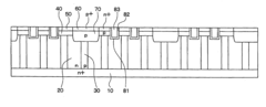
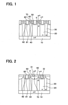
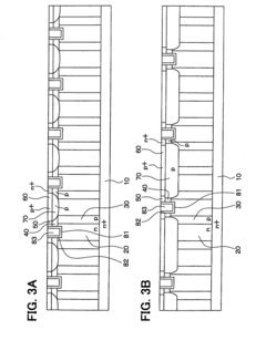
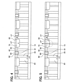
PatentInactiveUS20090267111A1
Innovation
- Integration of a Field Effect Rectifier (FER) into the MOSFET structure provides an alternative current path during switching, reducing carrier injection and minimizing EMI, while being compatible with conventional MOSFET technology and manufacturing processes.
Semiconductor device
PatentActiveUS20080283913A1
Innovation
- The semiconductor device incorporates a super junction structure with trench gate structures, a p-type body region, and specific impurity concentrations to direct avalanche current flow away from the source region, preventing parasitic bipolar transistor action by routing the current through a p+-type region and p-type body region, thereby enhancing avalanche capability.
Thermal Management Considerations in High-Performance Semiconductors
Thermal management represents a critical factor in the comparative analysis of P-N Junction and MOSFET technologies, particularly when evaluating their speed and energy efficiency characteristics. As semiconductor devices operate, they generate heat through various mechanisms including resistive heating and switching losses, which directly impacts their performance parameters.
P-N Junction devices typically exhibit simpler thermal profiles compared to MOSFETs due to their fundamental structure. The thermal conductivity of silicon in P-N junctions allows for relatively straightforward heat dissipation pathways. However, when operating at high frequencies, the junction temperature can rise significantly, leading to increased leakage currents and reduced efficiency. This thermal limitation becomes particularly evident in power applications where P-N junction diodes experience substantial forward voltage drops.
MOSFETs, conversely, present more complex thermal management challenges due to their multi-layered structure and higher integration densities. The channel region in MOSFETs can experience significant localized heating during high-frequency switching operations. This phenomenon, known as hot carrier injection, can degrade device performance over time and reduce operational lifespan if not properly managed.
Advanced cooling solutions have evolved specifically for high-performance semiconductor applications. For MOSFETs in particular, techniques such as flip-chip packaging, thermal vias, and integrated heat spreaders have become standard approaches to mitigate thermal constraints. These solutions enable MOSFETs to maintain their superior switching speeds even under demanding operational conditions.
The thermal coefficient of resistance represents another important consideration in the comparison. MOSFETs typically demonstrate a positive temperature coefficient, which helps distribute current more evenly across the device as temperature increases, providing an inherent form of thermal self-regulation. P-N junctions, however, often exhibit negative temperature coefficients that can lead to thermal runaway scenarios in certain applications.
Energy efficiency comparisons between these technologies must account for thermal management overhead. While MOSFETs offer lower conduction losses and faster switching capabilities, they may require more sophisticated cooling systems that consume additional energy. This creates a complex efficiency equation where the superior electrical performance of MOSFETs must be balanced against potentially higher thermal management requirements.
Recent innovations in semiconductor materials, such as silicon carbide (SiC) and gallium nitride (GaN), have significantly improved the thermal performance envelope for both technologies, allowing for higher operating temperatures and reduced cooling requirements. These wide-bandgap semiconductors demonstrate superior thermal conductivity properties that enhance both speed and energy efficiency metrics in high-performance applications.
Scaling Challenges and Moore's Law Implications
The semiconductor industry has long been guided by Moore's Law, which predicted the doubling of transistor density approximately every two years. However, as we approach physical limits in device scaling, both P-N junctions and MOSFETs face significant challenges that impact their speed and energy efficiency characteristics differently.
For P-N junctions, scaling challenges primarily manifest in increased junction capacitance and resistance as dimensions shrink. When junction areas decrease below certain thresholds, quantum tunneling effects become pronounced, leading to increased leakage currents that compromise energy efficiency. Additionally, as depletion regions narrow, breakdown voltage decreases, limiting power handling capabilities in scaled devices.
MOSFETs encounter more complex scaling issues due to their multi-layered structure. As gate lengths approach sub-10nm dimensions, short-channel effects become increasingly problematic, resulting in drain-induced barrier lowering and velocity saturation that degrade switching performance. The scaling of gate oxide thickness has essentially reached its limit with conventional materials, as quantum tunneling through ultra-thin oxides creates unacceptable leakage currents.
The implications for Moore's Law are profound. While MOSFET technology has managed to extend scaling through innovations like high-k dielectrics, metal gates, and FinFET architectures, these represent increasingly complex and costly solutions. The energy efficiency gains predicted by traditional scaling models have diminished, with static power consumption becoming a dominant factor in advanced nodes.
P-N junction-based devices, while simpler in structure, have not benefited as extensively from the scaling advantages that drove MOSFET dominance. However, this relative scaling disadvantage may become less significant as MOSFETs approach fundamental physical limits, potentially creating new opportunities for junction-based technologies in specific applications.
The economic implications of these scaling challenges cannot be overlooked. The capital expenditure required for each new process node has increased exponentially, forcing a consolidation in semiconductor manufacturing and raising questions about the sustainability of traditional scaling approaches. This economic reality has accelerated interest in alternative computing paradigms and specialized architectures that may rely differently on P-N junctions and MOSFETs.
Looking forward, the industry is exploring "More than Moore" strategies that focus on system-level integration rather than pure transistor scaling. This shift may rebalance the relative importance of P-N junction and MOSFET characteristics, with heterogeneous integration potentially leveraging the unique advantages of each technology where they provide optimal speed and energy efficiency.
Unlock deeper insights with Patsnap Eureka Quick Research — get a full tech report to explore trends and direct your research. Try now!
Generate Your Research Report Instantly with AI Agent
Supercharge your innovation with Patsnap Eureka AI Agent Platform!