Compare P–N Junctions: Signal Amplification vs. Noise Control
SEP 4, 20259 MIN READ
Generate Your Research Report Instantly with AI Agent
Patsnap Eureka helps you evaluate technical feasibility & market potential.
P-N Junction Technology Background and Objectives
P-N junctions represent one of the most fundamental structures in semiconductor technology, serving as the building blocks for numerous electronic devices since their discovery in the early 20th century. The evolution of P-N junction technology has been closely tied to the broader development of semiconductor physics, beginning with the theoretical work of Alan Wilson in the 1930s and the practical implementation by Russell Ohl at Bell Labs in 1940.
The technological trajectory of P-N junctions has been characterized by continuous refinement in material purity, fabrication techniques, and structural design. From the early germanium-based junctions to modern silicon and compound semiconductor implementations, each advancement has expanded the application scope and performance capabilities of these devices.
In the context of signal amplification versus noise control, P-N junctions play a dual and sometimes contradictory role. When configured in transistor arrangements, they enable signal amplification that forms the basis of modern electronics. Conversely, their inherent characteristics also introduce various noise sources that can degrade signal integrity, presenting a fundamental engineering challenge.
The primary objective in P-N junction development for signal processing applications is to optimize the signal-to-noise ratio (SNR) by enhancing amplification capabilities while minimizing noise generation and propagation. This balance represents a critical design consideration across applications ranging from telecommunications to scientific instrumentation.
Current technological goals focus on pushing the boundaries of P-N junction performance through novel materials, innovative junction geometries, and advanced fabrication techniques. Silicon carbide (SiC) and gallium nitride (GaN) junctions are being explored for their superior high-frequency performance and noise characteristics compared to traditional silicon implementations.
The emergence of nanoscale P-N junctions has opened new frontiers in both signal amplification and noise control. At these dimensions, quantum effects become significant, offering potential breakthroughs in amplification efficiency and noise suppression through quantum-limited operation.
Looking forward, the technology roadmap for P-N junctions aims to address the increasing demands of next-generation communication systems, high-precision sensing applications, and quantum computing interfaces. These applications require unprecedented levels of signal fidelity and noise immunity, driving research toward fundamental innovations in junction design and operation.
The convergence of P-N junction technology with other emerging fields, such as two-dimensional materials and topological insulators, presents promising avenues for overcoming current limitations in the signal amplification versus noise control paradigm, potentially enabling new classes of electronic devices with superior performance characteristics.
Market Applications and Demand Analysis
The P-N junction market has experienced significant growth in recent years, driven primarily by the expanding semiconductor industry. The global semiconductor market, where P-N junctions serve as fundamental components, reached approximately $556 billion in 2021 and is projected to grow at a CAGR of 7.8% through 2028. This growth directly impacts the demand for advanced P-N junction technologies that can balance signal amplification capabilities with effective noise control.
Consumer electronics represents the largest application segment for P-N junctions, accounting for nearly 40% of market demand. Within this segment, manufacturers increasingly require junctions that can provide high signal amplification while maintaining low noise profiles, particularly for smartphones, tablets, and wearable devices where power efficiency and signal clarity are paramount.
The automotive sector has emerged as the fastest-growing market for P-N junction applications, with the rise of electric vehicles and advanced driver-assistance systems (ADAS) creating unprecedented demand for high-performance semiconductor components. This sector particularly values P-N junctions with superior noise control characteristics to ensure reliable operation in safety-critical applications.
Medical device manufacturers constitute another significant market segment, where the demand for precision diagnostic equipment necessitates P-N junctions with exceptional signal-to-noise ratios. The global medical electronics market, valued at $73.2 billion in 2021, is expected to grow at 6.5% annually, creating substantial opportunities for specialized P-N junction technologies.
Telecommunications infrastructure development, particularly the ongoing global 5G rollout, has created strong demand for P-N junctions optimized for high-frequency applications where both signal amplification and noise suppression are critical performance factors. Industry analysts project that 5G-related semiconductor components will see a CAGR of 13.5% through 2026.
Regional analysis reveals that Asia-Pacific dominates the P-N junction market with approximately 65% share, led by manufacturing powerhouses in China, Taiwan, South Korea, and Japan. North America follows with roughly 20% market share, with particular strength in high-performance applications requiring advanced noise control capabilities.
Market surveys indicate that manufacturers are increasingly willing to pay premium prices for P-N junction technologies that offer demonstrable improvements in signal-to-noise ratios, with 78% of procurement specialists citing this as a key purchasing criterion. This trend suggests significant market potential for innovations that can push the boundaries of the traditional signal amplification versus noise control trade-off.
Current State and Technical Challenges
P-N junctions represent a fundamental building block in semiconductor technology, serving dual critical functions in signal amplification and noise control. Currently, the global semiconductor industry has achieved significant advancements in P-N junction technology, with feature sizes reaching below 5nm in commercial applications. However, as devices continue to miniaturize, quantum effects increasingly dominate junction behavior, creating new challenges for traditional semiconductor physics models.
The state-of-the-art P-N junction technology demonstrates remarkable capabilities in signal amplification, with modern transistors achieving gain factors exceeding 1000 in optimal configurations. This performance enables the complex signal processing required in today's advanced computing and communications systems. However, as operating frequencies push into the terahertz range, parasitic capacitance effects increasingly limit amplification efficiency.
Noise control represents perhaps the most significant current challenge in P-N junction technology. As junction dimensions shrink, thermal noise, shot noise, and flicker noise become increasingly prominent, degrading signal integrity. Recent research indicates that in sub-10nm junctions, noise can reduce the effective signal-to-noise ratio by up to 40% compared to theoretical limits, particularly at elevated temperatures or in high-radiation environments.
Geographically, P-N junction technology development shows distinct regional characteristics. East Asian manufacturers, particularly in Taiwan and South Korea, lead in high-volume production techniques, while North American and European research institutions focus on novel materials and junction architectures. China has rapidly expanded its semiconductor capabilities, though still lags in cutting-edge junction technology by approximately 2-3 generations.
A significant technical constraint facing P-N junction development is the increasing difficulty in maintaining precise dopant profiles at nanoscale dimensions. Ion implantation techniques struggle to achieve uniform doping at these scales, leading to junction variability that impacts both amplification consistency and noise characteristics. Recent advances in atomic layer deposition offer promising alternatives but remain challenging to scale commercially.
Power dissipation presents another critical challenge, particularly for signal amplification applications. As junction density increases, thermal management becomes increasingly problematic, with current high-performance chips generating heat fluxes exceeding 100 W/cm². This thermal constraint directly impacts noise performance, creating a complex engineering trade-off between amplification capability and noise control.
Material limitations also constrain further advancement, with silicon approaching its theoretical performance limits. While compound semiconductors like gallium nitride and silicon carbide offer superior properties for specific applications, their integration with conventional silicon processes remains technically challenging and economically prohibitive for many applications.
Signal Amplification vs. Noise Control Solutions
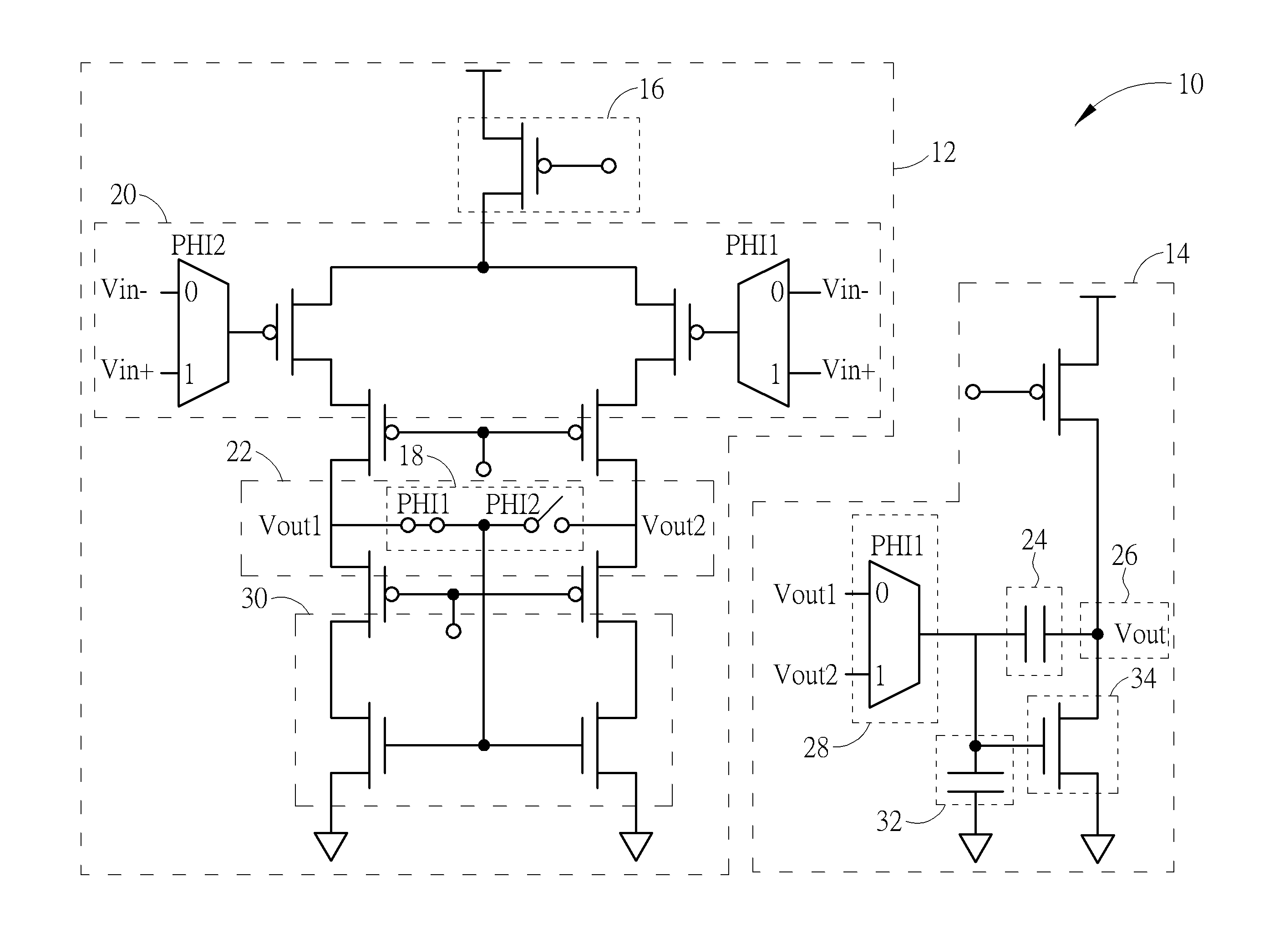
01 Transistor-based signal amplification techniques
P-N junction transistors are widely used for signal amplification in electronic circuits. These devices leverage the properties of semiconductor junctions to control current flow and achieve gain. Various circuit configurations, including common emitter, common base, and common collector arrangements, can be implemented to optimize amplification characteristics while maintaining signal integrity. Advanced designs incorporate feedback mechanisms to stabilize operation across temperature variations and input conditions.- Semiconductor amplifier designs using P-N junctions: Various semiconductor amplifier designs utilize P-N junctions for signal amplification. These designs incorporate specific circuit configurations to enhance signal strength while maintaining signal integrity. The amplifiers may use multiple P-N junction stages to achieve higher gain levels and can be optimized for different frequency ranges. These designs often include feedback mechanisms to stabilize operation and improve linearity.
- Noise reduction techniques in P-N junction devices: Various techniques are employed to reduce noise in P-N junction-based electronic devices. These include specialized biasing methods, thermal noise compensation circuits, and isolation strategies to minimize interference. Some approaches involve optimizing the physical structure of the P-N junction itself to reduce inherent noise generation. Advanced filtering techniques may also be implemented to separate desired signals from noise components.
- Optical signal processing with P-N junction devices: P-N junctions are utilized in optical signal processing applications for amplification and noise control. These devices convert optical signals to electrical signals, process them, and may convert them back to optical form. The technology enables efficient handling of optical communications with minimal signal degradation. Various designs incorporate specialized P-N junction structures optimized for optical wavelengths and signal characteristics.
- Testing and measurement systems for P-N junction performance: Specialized testing and measurement systems are designed to evaluate the performance of P-N junction devices in signal amplification and noise control applications. These systems can characterize parameters such as gain, noise figure, linearity, and frequency response. Advanced measurement techniques allow for precise evaluation of junction behavior under various operating conditions, enabling optimization of device design and manufacturing processes.
- Novel P-N junction structures for enhanced signal processing: Innovative P-N junction structures are developed to enhance signal processing capabilities. These include specialized doping profiles, multi-layer junctions, and nano-scale designs that improve amplification efficiency and reduce noise. Some structures incorporate additional materials or geometric configurations to optimize electrical characteristics. These novel designs aim to overcome traditional limitations of P-N junction devices in high-frequency or high-power applications.
02 Noise reduction in P-N junction devices
Controlling noise in P-N junction-based amplifiers is critical for maintaining signal quality. Techniques include optimized biasing methods, careful junction design to minimize thermal noise, and specialized circuit topologies that cancel common-mode noise. Differential amplifier configurations are particularly effective at rejecting noise while maintaining signal fidelity. Additional approaches involve shielding, proper grounding techniques, and the use of low-noise semiconductor materials in the junction fabrication process.Expand Specific Solutions03 Optical signal processing with P-N junctions
P-N junctions are employed in photodiodes and other optoelectronic devices for converting optical signals to electrical signals and subsequent amplification. These devices utilize the photovoltaic effect at the junction to generate carriers when exposed to light. Advanced designs incorporate specialized junction geometries to enhance quantum efficiency and response time. Signal processing techniques specific to optical applications include transimpedance amplification stages and specialized filtering to extract signals from noise in low-light conditions.Expand Specific Solutions04 Advanced semiconductor materials for improved junction performance
The performance of P-N junction-based amplifiers can be significantly enhanced through the use of specialized semiconductor materials and fabrication techniques. Compound semiconductors like gallium arsenide and silicon germanium offer superior electron mobility compared to traditional silicon, resulting in higher frequency operation and lower noise characteristics. Heterojunction designs that combine different semiconductor materials can optimize both carrier transport and energy band characteristics, leading to improved amplification efficiency and noise immunity.Expand Specific Solutions05 Testing and measurement of P-N junction amplifier characteristics
Specialized testing methodologies have been developed to characterize the performance of P-N junction-based amplifiers. These include techniques for measuring gain, bandwidth, noise figure, and linearity parameters. Advanced measurement systems can isolate junction-specific characteristics from overall circuit behavior, enabling optimization of the semiconductor structure itself. Automated testing platforms incorporate temperature control and precise signal generation to ensure consistent and accurate performance evaluation across operating conditions.Expand Specific Solutions
Key Industry Players and Competition Landscape
The P-N junction technology market is currently in a mature growth phase, with an estimated global market size exceeding $25 billion. Major semiconductor players like Samsung Electronics, MediaTek, and NXP Semiconductors dominate the signal amplification segment, while specialized companies such as Himax Technologies and PixArt Imaging focus on noise control innovations. Technology maturity varies across applications - signal amplification technologies are well-established with incremental improvements, while noise control solutions are experiencing more rapid innovation, particularly in high-frequency applications. Apple and Google are increasingly investing in proprietary P-N junction technologies for their consumer electronics, while automotive applications are being advanced by Toyota, Honda, and Robert Bosch for electric vehicle power management systems.
Samsung Electronics Co., Ltd.
Technical Solution: Samsung has developed advanced P-N junction technology for their semiconductor devices focusing on signal amplification with minimal noise interference. Their approach involves utilizing specialized doping profiles in silicon to create optimized junction characteristics. Samsung's P-N junction designs incorporate gradient doping techniques that create a more gradual transition region, reducing capacitance effects while maintaining high conductivity. For signal amplification applications, they've implemented selective epitaxial growth processes to create ultra-thin junction regions with precisely controlled impurity concentrations. This enables higher transconductance in their transistor designs while minimizing junction capacitance that contributes to noise. Samsung has also pioneered the use of germanium-silicon alloys at junction interfaces to enhance carrier mobility and reduce thermal noise generation[1].
Strengths: Samsung's extensive manufacturing infrastructure allows for precise control of doping profiles and junction formation. Their technology excels in high-frequency applications where signal integrity is critical. Weaknesses: Their solutions tend to be more expensive than competitors and may require more complex fabrication processes, limiting applicability in cost-sensitive applications.
Apple, Inc.
Technical Solution: Apple has developed proprietary P-N junction technology specifically optimized for their mobile and computing devices, focusing on the critical balance between signal amplification and noise control. Their approach centers on custom-designed semiconductor architectures that utilize advanced junction engineering techniques. Apple's P-N junction designs feature ultra-shallow junction depths with highly controlled doping gradients to minimize parasitic capacitance while maintaining excellent carrier transport properties. For their high-performance processors, Apple employs specialized annealing techniques that activate dopants while minimizing diffusion, creating abrupt junctions that enhance signal amplification capabilities. Their noise control strategy incorporates innovative guard ring structures surrounding sensitive junction areas to isolate noise sources and prevent cross-talk between adjacent components. Additionally, Apple has implemented proprietary passivation techniques at junction surfaces to reduce interface states that contribute to 1/f noise[2][3].
Strengths: Apple's vertical integration allows them to optimize P-N junctions specifically for their product ecosystem, resulting in excellent power efficiency and signal integrity. Their designs excel in mixed-signal environments where analog and digital circuits must coexist. Weaknesses: Their highly specialized approach may not be broadly applicable to other applications, and their technology is largely kept proprietary rather than shared with the industry.
Critical Patents and Technical Literature Review
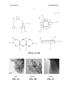
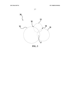
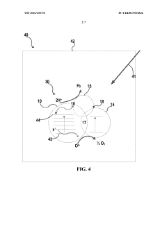
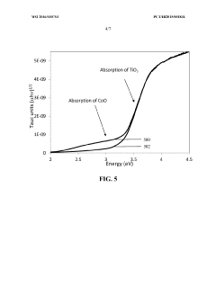
Photocatalytic hydrogen production from water over catalysts having p-n juncations and plasmonic materials
PatentWO2016030753A1
Innovation
- A photocatalyst combining a p-n junction formed by an n-type semiconductor material, such as titanium dioxide, with a p-type semiconductor and metal or metal alloy having surface plasmon resonance properties, which increases charge carrier lifetime and reduces recombination, allowing for efficient hydrogen and oxygen production without external bias or voltage.
Signal amplifying circuit with noise suppression function
PatentActiveUS20170019073A1
Innovation
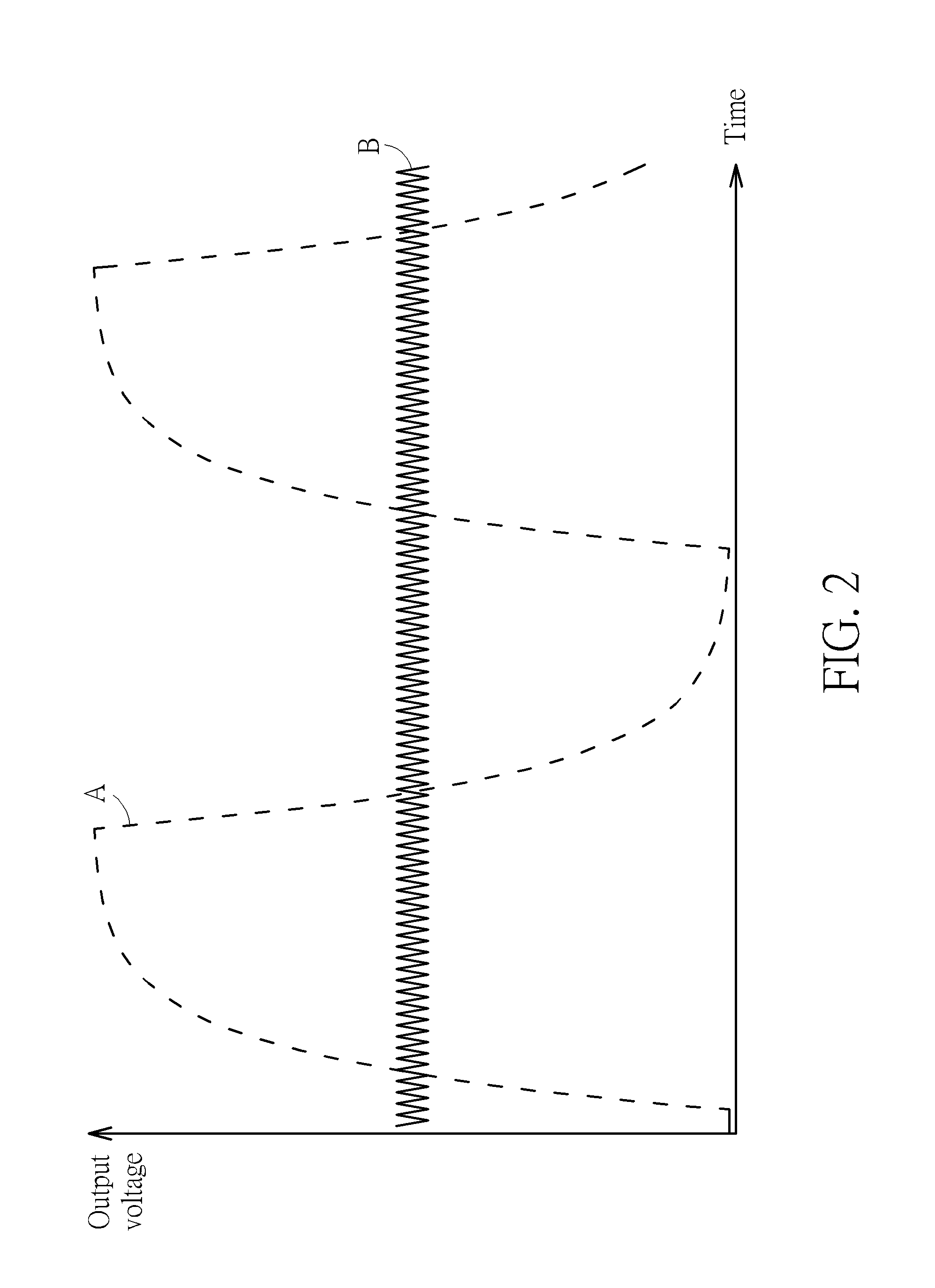
- A signal amplifying circuit with a first and second circuit module, where the interior frequency bandwidth is adjusted by controlling the current source and equivalent capacitance, with the chopping frequency at least 10 times the bandwidth, allowing for effective suppression of direct current offset and low-frequency noise through slew rate-driven switching.
Semiconductor Manufacturing Process Considerations
The manufacturing process of P-N junctions significantly impacts their performance characteristics in both signal amplification and noise control applications. Precision in doping concentration and profile control represents a critical factor, as it directly influences the junction's electrical properties. Higher doping concentrations typically enhance conductivity and signal strength but may simultaneously increase noise generation through shot noise mechanisms. Conversely, carefully controlled moderate doping levels can optimize the signal-to-noise ratio for sensitive detection applications.
Junction depth and geometry considerations present another manufacturing challenge with substantial performance implications. Shallow junctions favor high-frequency operation and reduced capacitance, beneficial for signal amplification in RF applications. However, these shallow structures often exhibit increased susceptibility to surface noise effects. Deeper junctions demonstrate superior thermal stability and noise immunity but may compromise high-frequency response due to increased capacitance.
Material purity during manufacturing emerges as a paramount concern for noise-sensitive applications. Crystal defects, impurities, and lattice dislocations introduce generation-recombination centers that contribute to excess noise, particularly at lower frequencies where 1/f noise dominates. Ultra-high-purity silicon processing with controlled oxygen content becomes essential for low-noise applications, while signal amplification circuits may tolerate slightly higher defect densities.
Thermal management considerations during manufacturing directly impact both performance domains. Thermal gradients during processing can create stress-induced defects that manifest as noise sources during operation. Advanced annealing techniques and temperature-controlled processing steps help minimize these effects. For high-power amplification applications, thermal considerations extend to package design and heat dissipation capabilities to prevent thermal noise amplification during operation.
Surface passivation quality represents a critical manufacturing consideration often overlooked. Inadequate surface passivation leads to increased surface leakage currents and noise generation at the semiconductor-oxide interface. Advanced passivation techniques using precisely controlled oxide growth or nitride deposition significantly reduce surface-state density, benefiting both signal integrity and noise performance. This aspect becomes particularly crucial for modern miniaturized devices where surface-to-volume ratios increase dramatically.
Manufacturing process variations inevitably lead to device parameter spread, affecting both amplification characteristics and noise performance. Statistical process control methodologies and advanced metrology techniques help maintain tight parameter distributions, ensuring consistent performance across production batches. For noise-critical applications, additional screening and binning procedures may be implemented to select devices with optimal noise characteristics from standard production runs.
Performance Metrics and Testing Methodologies
Evaluating the performance of P-N junctions in both signal amplification and noise control applications requires comprehensive metrics and standardized testing methodologies. These assessment frameworks enable engineers to make informed decisions when selecting appropriate junction configurations for specific electronic applications.
Signal-to-Noise Ratio (SNR) stands as the primary metric for comparing junction performance, quantifying the relationship between desired signal strength and unwanted noise. For amplification applications, gain measurements including voltage gain, current gain, and power gain provide critical insights into junction efficiency. Frequency response testing reveals bandwidth limitations, with cutoff frequencies and gain-bandwidth products serving as key performance indicators.
Noise figure measurements quantify the degradation of SNR as signals pass through P-N junction devices. Lower noise figures indicate superior noise performance, with specialized equipment like spectrum analyzers and noise figure meters enabling precise characterization. Temperature coefficient testing evaluates stability across operating conditions, as junction characteristics vary significantly with temperature fluctuations.
Linearity testing assesses distortion characteristics through metrics such as Total Harmonic Distortion (THD) and Intermodulation Distortion (IMD). These measurements are particularly relevant for signal amplification applications where signal integrity must be maintained. Power efficiency metrics, including power consumption and heat dissipation, help determine operational costs and cooling requirements.
Standardized testing protocols ensure consistency across evaluations. IEEE standards for semiconductor device testing provide frameworks for junction characterization, while JEDEC standards address reliability aspects. These protocols typically involve controlled environmental conditions with temperature chambers maintaining precise thermal environments during testing.
Automated test equipment (ATE) systems enable high-throughput characterization of multiple parameters simultaneously. These systems incorporate precision current sources, voltage meters, and temperature controllers to ensure measurement accuracy. Statistical analysis of test results, including Monte Carlo simulations, helps quantify manufacturing variations and predict real-world performance distributions.
Accelerated life testing methodologies subject junctions to elevated stress conditions to predict long-term reliability. These tests include temperature cycling, bias-temperature stress, and electrostatic discharge (ESD) testing. The resulting data enables calculation of Mean Time Between Failures (MTBF) and other reliability metrics essential for applications requiring sustained performance over extended periods.
Unlock deeper insights with Patsnap Eureka Quick Research — get a full tech report to explore trends and direct your research. Try now!
Generate Your Research Report Instantly with AI Agent
Supercharge your innovation with Patsnap Eureka AI Agent Platform!