P–N Junction Adaptation in Next-Gen Electronics
SEP 5, 202510 MIN READ
Generate Your Research Report Instantly with AI Agent
PatSnap Eureka helps you evaluate technical feasibility & market potential.
P-N Junction Evolution and Development Goals
The P-N junction, first theorized by Russell Ohl in 1939 and demonstrated in 1940, represents one of the most fundamental structures in semiconductor physics. Its discovery revolutionized electronics by enabling the development of diodes, transistors, and integrated circuits that form the backbone of modern electronic devices. The evolution of P-N junction technology has been closely tied to the advancement of semiconductor materials, fabrication techniques, and device architectures over the past eight decades.
In the early stages (1940s-1950s), P-N junctions were primarily implemented in germanium, with relatively simple fabrication processes and limited performance capabilities. The transition to silicon in the late 1950s marked a significant milestone, offering improved thermal stability and enabling more reliable semiconductor devices. The 1960s-1970s witnessed the refinement of junction formation techniques, including diffusion and ion implantation, which allowed for more precise control over dopant profiles and junction characteristics.
The miniaturization trend that began in the 1980s pushed P-N junctions to smaller dimensions, necessitating innovations in fabrication technology to maintain performance as devices scaled down. This era saw the introduction of shallow junctions, improved contact metallization, and enhanced isolation techniques to prevent parasitic effects in increasingly dense integrated circuits.
Recent decades have witnessed the exploration of P-N junctions in novel semiconductor materials beyond silicon, including compound semiconductors (GaAs, GaN, SiC), wide bandgap materials, and two-dimensional materials like graphene and transition metal dichalcogenides. These materials offer advantages such as higher electron mobility, better high-frequency performance, and operation under extreme conditions.
The current technological trajectory aims to adapt P-N junctions for next-generation electronics that demand unprecedented performance metrics. Key development goals include reducing junction leakage current to minimize power consumption in ultra-low-power applications, enhancing switching speeds for high-frequency operations, and improving thermal stability for robust performance in harsh environments.
Another critical objective is the seamless integration of P-N junctions with emerging technologies such as flexible electronics, transparent displays, and bioelectronic interfaces. This requires developing junction formation techniques compatible with temperature-sensitive substrates and establishing reliable electrical connections between dissimilar materials.
Looking forward, the evolution of P-N junctions will likely focus on achieving atomic-scale precision in junction formation, exploring quantum effects in nanoscale junctions, and developing novel architectures that leverage heterogeneous material integration. The ultimate goal is to extend the capabilities of P-N junctions beyond traditional electronic applications into emerging fields such as neuromorphic computing, quantum information processing, and energy harvesting systems.
Market Analysis for Advanced Semiconductor Applications
The global market for advanced semiconductor applications leveraging P-N junction technology is experiencing unprecedented growth, driven by the proliferation of next-generation electronics across multiple sectors. Current market valuations indicate that the semiconductor industry centered around advanced junction technologies reached approximately $550 billion in 2023, with projections suggesting a compound annual growth rate of 7.8% through 2028.
The demand landscape for P-N junction adaptations is particularly robust in several key sectors. The consumer electronics segment remains the largest market driver, accounting for nearly 40% of total demand, with smartphones and portable computing devices leading consumption. However, the automotive sector is emerging as the fastest-growing application area, with demand for power semiconductors and sensing devices increasing at nearly 12% annually as electric vehicles and advanced driver assistance systems become mainstream.
Industrial applications represent another significant growth vector, particularly in factory automation, where intelligent power modules based on advanced junction technologies are enabling more efficient motor control systems and power conversion. This segment is growing at approximately 9% annually, driven by Industry 4.0 initiatives worldwide.
Regional analysis reveals shifting dynamics in the market for advanced P-N junction applications. While North America and Europe have traditionally dominated in terms of technology development, Asia-Pacific now represents over 60% of the global manufacturing capacity for these components, with China, Taiwan, and South Korea making substantial investments in domestic semiconductor capabilities.
Market research indicates that miniaturization trends are creating substantial demand for novel P-N junction architectures. The average transistor density in leading-edge chips has increased by approximately 30% year-over-year, necessitating innovations in junction design to manage thermal issues and quantum effects at nanoscale dimensions.
Energy efficiency has emerged as a critical market driver, with data centers alone consuming over 1% of global electricity. This has created a premium market segment for wide-bandgap semiconductors with specialized P-N junction configurations that can operate at higher temperatures and voltages while reducing energy losses by up to 40% compared to traditional silicon-based alternatives.
Customer requirements analysis shows increasing demand for radiation-hardened P-N junction devices in aerospace and defense applications, a niche but high-margin segment growing at approximately 6% annually. Similarly, medical electronics represents an emerging application area, with implantable devices and diagnostic equipment requiring specialized junction technologies that can operate reliably within biological environments.
Current P-N Junction Technology Limitations
Despite significant advancements in semiconductor technology, P-N junctions face several critical limitations that impede their adaptation for next-generation electronics. The fundamental scaling constraints have become increasingly problematic as devices approach nanometer dimensions. When P-N junctions are scaled below 10nm, quantum tunneling effects become pronounced, leading to increased leakage currents that compromise device performance and energy efficiency. This tunneling phenomenon creates a physical barrier to further miniaturization, challenging Moore's Law continuation.
Thermal management represents another significant limitation. As device density increases, power dissipation per unit area rises dramatically, creating hotspots that can reach temperatures exceeding 100°C during operation. These thermal issues not only reduce reliability but also necessitate complex cooling solutions that add cost and design complexity to electronic systems.
The interface quality between P and N regions presents persistent manufacturing challenges. Current fabrication techniques struggle to create atomically sharp interfaces with minimal defects when working at advanced nodes. These interface imperfections lead to carrier recombination centers that degrade electrical characteristics and reduce overall device efficiency. Even state-of-the-art processes typically introduce defect densities of 10^8-10^10 cm^-2 at the junction interface.
Conventional P-N junctions also exhibit relatively slow switching speeds due to inherent capacitance and minority carrier storage effects. The charge storage phenomenon limits frequency response to the gigahertz range, which is increasingly insufficient for applications in terahertz computing and ultra-fast communications systems being developed for 6G and beyond.
Material limitations further constrain P-N junction performance. Silicon-based junctions have nearly reached their theoretical performance limits regarding bandgap engineering and carrier mobility. While compound semiconductors offer improved characteristics, they introduce significant manufacturing complexity and cost increases, typically 3-5 times higher than silicon-based processes.
Voltage constraints represent another critical limitation. Traditional P-N junctions in silicon typically operate below 5V for small-signal applications, with specialized high-voltage designs reaching only 50-100V before breakdown occurs. This restricts their application in emerging power electronics and high-voltage applications necessary for renewable energy systems and electric vehicles.
Finally, P-N junctions demonstrate limited flexibility for integration with emerging materials such as 2D semiconductors, organic electronics, and quantum materials. The rigid crystalline structure requirements of conventional junctions create compatibility challenges with these novel material systems, hindering the development of hybrid electronic platforms that could enable entirely new device functionalities.
Contemporary P-N Junction Implementation Approaches
01 Basic P-N Junction Structure and Functionality
P-N junctions are fundamental semiconductor structures formed by joining p-type and n-type semiconductor materials. These junctions create a depletion region at the interface where charge carriers diffuse across the junction, establishing an electric field. This basic structure is the foundation for various semiconductor devices including diodes, transistors, and solar cells. The electrical characteristics of P-N junctions, particularly their ability to conduct current in one direction while blocking it in the other, make them essential components in modern electronics.- P-N Junction Structure and Fabrication: P-N junctions are fundamental semiconductor structures formed by joining p-type and n-type semiconductor materials. The fabrication process involves doping techniques to create regions with different charge carriers. These junctions form the basis for various electronic devices including diodes, transistors, and integrated circuits. The interface between p and n regions creates a depletion region that is crucial for the junction's electrical properties.
- P-N Junction in Solar Cell Applications: P-N junctions are essential components in photovoltaic cells, where they facilitate the conversion of light energy into electrical energy. When photons strike the junction, they generate electron-hole pairs that are separated by the built-in electric field at the junction. This separation of charges creates a voltage difference that can be harnessed as electrical power. Various designs and materials are used to optimize the efficiency of solar cells based on P-N junction technology.
- P-N Junction in Power Electronics: In power electronic applications, P-N junctions are utilized in devices such as power diodes, thyristors, and transistors. These components handle high voltages and currents for power conversion and control. The junction characteristics determine the blocking voltage, forward current capability, and switching performance. Advanced designs incorporate features to enhance thermal management and reliability under high-power conditions.
- P-N Junction in Sensing and Detection: P-N junctions are employed in various sensing and detection applications, including photodetectors, temperature sensors, and radiation detectors. The junction's sensitivity to external stimuli like light, temperature, or radiation causes measurable changes in its electrical properties. These changes can be amplified and processed to provide information about the environment. Different semiconductor materials are selected based on the specific sensing requirements.
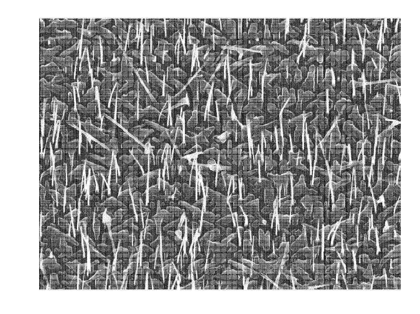
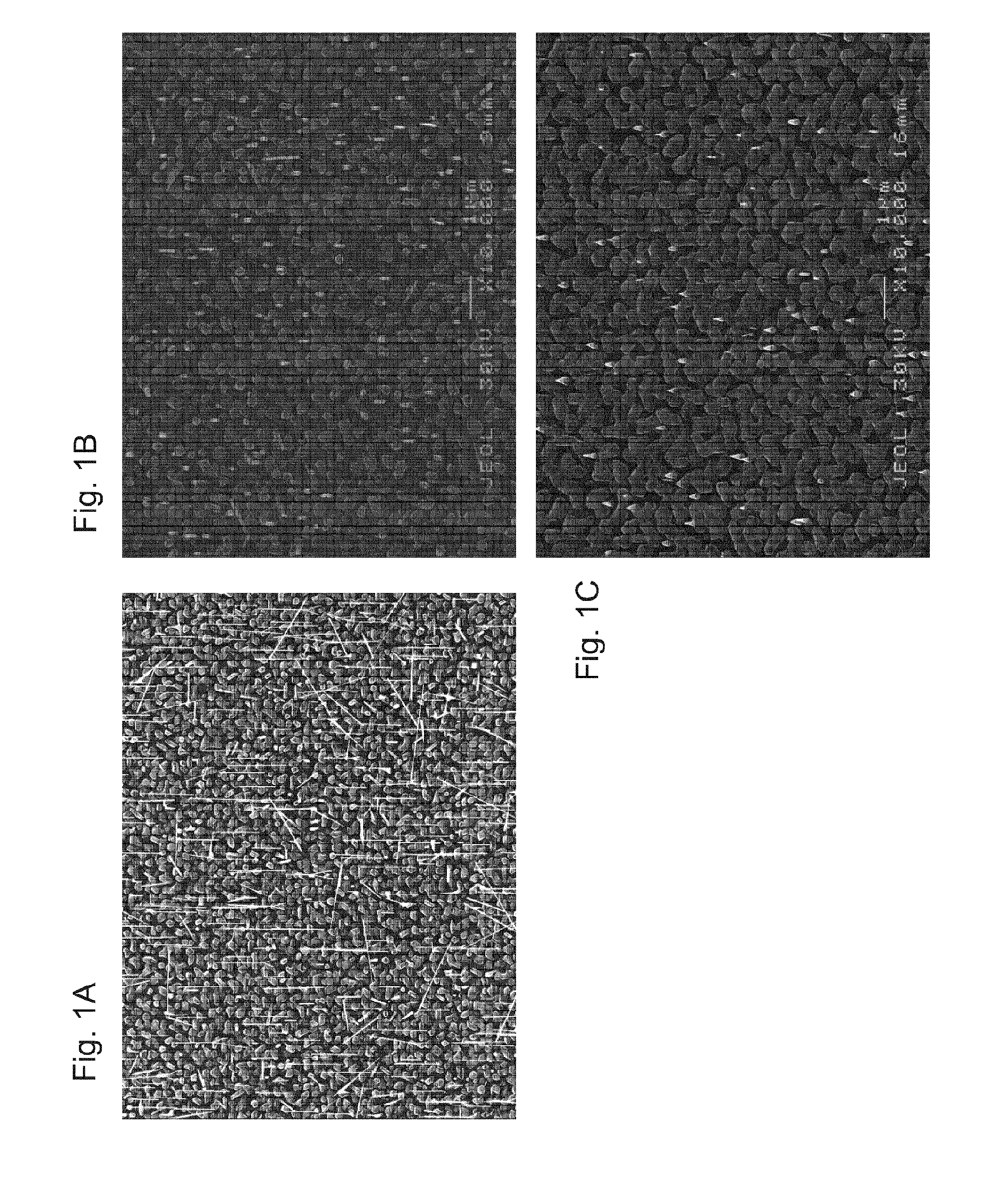
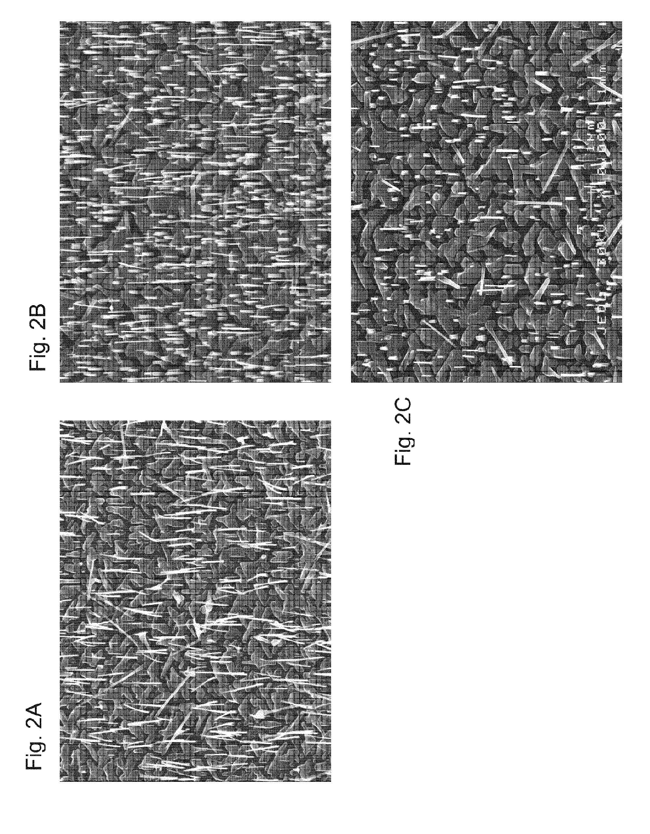
- Novel P-N Junction Materials and Structures: Research in P-N junction technology includes the development of novel materials and junction structures to enhance performance and enable new applications. This includes heterojunctions (junctions between different semiconductor materials), nanoscale junctions, and junctions incorporating 2D materials or quantum structures. These innovations aim to overcome limitations of traditional silicon-based junctions and enable advancements in electronics, optoelectronics, and energy conversion technologies.
02 P-N Junction Applications in Solar Cells
P-N junctions are widely used in photovoltaic applications where they convert light energy into electrical energy. When photons strike the junction, they generate electron-hole pairs that are separated by the built-in electric field, producing a photocurrent. Advanced solar cell designs incorporate multiple junctions, specialized doping profiles, and surface treatments to enhance efficiency and power output. These improvements focus on optimizing light absorption, reducing recombination losses, and improving charge carrier collection.Expand Specific Solutions03 P-N Junction in Power Electronics and Devices
In power electronic applications, P-N junctions are engineered to handle high voltages and currents. These specialized junctions incorporate features such as wide bandgap materials, edge termination structures, and field plates to enhance breakdown voltage and reduce leakage current. Power devices utilizing these junctions include power diodes, thyristors, and insulated gate bipolar transistors (IGBTs). The design focuses on minimizing on-state losses, improving switching performance, and enhancing thermal management to ensure reliable operation under high-power conditions.Expand Specific Solutions04 Advanced P-N Junction Manufacturing Techniques
Modern semiconductor fabrication employs sophisticated techniques to create precisely controlled P-N junctions. These methods include ion implantation, epitaxial growth, diffusion processes, and advanced annealing techniques. Recent innovations focus on creating ultra-shallow junctions for nanoscale devices, three-dimensional junction architectures, and heterojunctions between different semiconductor materials. These manufacturing advances enable the production of high-performance semiconductor devices with improved electrical characteristics and reliability.Expand Specific Solutions05 P-N Junction Integration in Novel Applications
P-N junctions are being integrated into emerging technologies beyond traditional semiconductor devices. These applications include sensors, detectors, quantum computing elements, and bioelectronic interfaces. Novel junction designs incorporate nanomaterials, organic semiconductors, and hybrid structures to achieve specialized functionalities. Research focuses on exploiting quantum effects, enhancing sensitivity to external stimuli, and developing flexible or transparent junction-based devices for next-generation electronics.Expand Specific Solutions
Leading Semiconductor Manufacturers and Research Institutions
The P-N junction adaptation market in next-generation electronics is currently in a growth phase, with an expanding market size driven by increasing demand for advanced semiconductor solutions. The technology is approaching maturity but continues to evolve, with major players driving innovation across different application segments. Industry leaders like Taiwan Semiconductor Manufacturing Co., IBM, and NXP Semiconductors are advancing commercial applications, while research institutions including Arizona State University, National University of Singapore, and Oxford University are pioneering fundamental breakthroughs. Sharp Corp. and Infineon Technologies are focusing on consumer electronics applications, while specialized firms like Nanoco Technologies and Novaled GmbH are developing niche solutions for emerging markets. The competitive landscape reflects a balance between established semiconductor manufacturers and research-focused entities collaborating to address technical challenges in miniaturization and efficiency.
International Business Machines Corp.
Technical Solution: IBM has developed groundbreaking P-N junction adaptation technologies for next-generation electronics focusing on quantum computing and neuromorphic applications. Their approach utilizes atomic-precision doping techniques through scanning tunneling microscopy to create deterministic single-atom P-N junctions with unprecedented control over quantum states[1]. IBM has pioneered the integration of 2D materials like graphene and transition metal dichalcogenides (TMDs) to form atomically thin P-N junctions with unique electronic properties. Their research includes the development of vertical heterojunction structures that leverage band alignment engineering to create novel electronic and optoelectronic functionalities[3]. IBM's advanced junction technology incorporates strain engineering at the atomic scale to modulate bandgap properties and carrier mobility. They have also developed specialized junction architectures for neuromorphic computing that mimic synaptic behavior through controlled defect engineering and interface states[5]. Their approach includes innovative methods for creating abrupt junction profiles using molecular beam epitaxy and atomic layer deposition techniques, enabling quantum confinement effects to be exploited in next-generation computing paradigms.
Strengths: Unparalleled precision in atomic-scale junction formation. Leading expertise in quantum effects at junction interfaces. Advanced capabilities in heterojunction engineering for novel device concepts. Weaknesses: Extremely high manufacturing complexity with current techniques not readily scalable to high-volume production. Some approaches remain primarily in research phase rather than production-ready technologies.
Novaled GmbH
Technical Solution: Novaled has developed specialized P-N junction adaptation technologies focused on organic and hybrid semiconductor applications for next-generation electronics. Their proprietary PIN (p-type, intrinsic, n-type) architecture optimizes charge carrier transport across organic semiconductor junctions through precisely controlled doping profiles[2]. Novaled's technology incorporates molecular doping techniques that enable fine-tuning of energy levels at organic-organic and organic-inorganic interfaces, significantly improving charge injection and extraction efficiency[4]. They have pioneered the development of ultra-stable p-type and n-type dopants that maintain junction characteristics over extended operational lifetimes, addressing a critical challenge in organic electronics. Their approach includes specialized interface engineering methods that minimize energetic barriers at heterojunctions through the introduction of dipole layers and gradient doping profiles[6]. Novaled has also developed innovative encapsulation technologies that protect sensitive junction regions from environmental degradation, enhancing long-term stability. Their junction optimization techniques have enabled record-breaking performance in OLED displays with improved power efficiency and extended operational lifetimes.
Strengths: Industry-leading expertise in organic semiconductor junction engineering. Superior charge transport optimization through molecular doping techniques. Excellent control over interface energetics for improved device performance. Weaknesses: Some approaches remain sensitive to environmental factors despite encapsulation. Higher manufacturing complexity compared to conventional inorganic semiconductor processing.
Key Patents and Breakthroughs in Junction Engineering
Electronic component with at least one organic layer
PatentActiveEP1808910A2
Innovation
- The use of np/n junctions with p-type and n-type organic semiconductor materials in contact with conductive layers of the anode and cathode, respectively, allows for efficient generation of free charge carriers and flexibility in selecting electrode materials, improving charge carrier balance and efficiency.


Nanostructure, nanostructure fabrication method, and photovoltaic cell incorporating a nanostructure
PatentInactiveUS20140283901A1
Innovation
- The development of gallium-assisted growth methods for GaAsP nanostructures, which involves controlling the chemical potential of gallium droplets to supersaturate with both arsenic and phosphorous, allowing for the formation of Au-free GaAsP nanostructures with improved purity and uniformity, and using molecular beam epitaxy or metalorganic vapour-phase epitaxy to achieve specific band gaps and doping during growth.

Materials Science Advancements for Enhanced Junction Performance
Recent advancements in materials science have revolutionized P-N junction performance in next-generation electronics. Traditional silicon-based junctions are increasingly being supplemented or replaced by novel materials that offer superior electrical properties, enhanced carrier mobility, and improved thermal stability. Compound semiconductors such as gallium nitride (GaN) and silicon carbide (SiC) have emerged as frontrunners for high-power and high-frequency applications, demonstrating breakdown voltages up to ten times higher than conventional silicon while maintaining excellent thermal conductivity.
The integration of two-dimensional materials represents another significant breakthrough in junction technology. Graphene, with its exceptional electron mobility exceeding 200,000 cm²/Vs at room temperature, enables ultra-fast switching speeds when incorporated into heterojunction designs. Similarly, transition metal dichalcogenides (TMDs) like MoS2 and WSe2 offer atomically thin semiconducting layers with direct bandgaps, facilitating more efficient optical and electronic properties at nanoscale dimensions.
Bandgap engineering through material composition tuning has become increasingly sophisticated, allowing precise control over junction characteristics. The development of quaternary alloys such as InGaAsP and AlInGaP permits continuous adjustment of bandgap energies across a wide spectrum, enabling customized junction properties for specific applications ranging from photovoltaics to optoelectronics.
Surface passivation techniques have advanced considerably, addressing the persistent challenge of interface states that degrade junction performance. Atomic layer deposition (ALD) of high-k dielectrics has proven particularly effective in reducing interface trap densities by orders of magnitude, while simultaneously providing excellent conformality even on complex three-dimensional structures.
Strain engineering has emerged as a powerful approach to modifying band structures and enhancing carrier mobility. Controlled introduction of tensile or compressive strain through lattice-mismatched epitaxial growth or mechanical methods can significantly alter electronic properties, with mobility enhancements of up to 400% demonstrated in certain strained silicon configurations.
Nanomaterials and quantum structures have introduced new paradigms in junction design. Quantum dots, nanowires, and nanotubes exhibit quantum confinement effects that dramatically alter electronic and optical properties compared to bulk materials. These structures enable precise control over energy levels and carrier dynamics, facilitating novel junction behaviors including multiple exciton generation and hot carrier extraction.
The incorporation of organic-inorganic hybrid materials, particularly metal-halide perovskites, has created new possibilities for flexible and low-cost junction fabrication. These materials combine solution processability with impressive electronic properties, achieving power conversion efficiencies exceeding 25% in photovoltaic applications while offering tunable bandgaps through compositional engineering.
Environmental Impact of Next-Gen Semiconductor Manufacturing
The evolution of P-N junction technology in next-generation electronics presents significant environmental challenges and opportunities within semiconductor manufacturing processes. Traditional semiconductor fabrication involves extensive use of hazardous chemicals, heavy metals, and rare earth elements that pose substantial environmental risks. The transition to advanced P-N junction architectures in next-generation devices requires even more complex manufacturing processes, potentially increasing the environmental footprint if not managed properly.
Water consumption represents a critical environmental concern, with a single semiconductor facility consuming up to 4-5 million gallons daily. Next-generation P-N junction fabrication processes often require ultra-pure water for cleaning and processing, exacerbating water scarcity issues in manufacturing regions. Additionally, the chemical waste generated contains toxic compounds including arsenic, antimony, and phosphorus dopants used specifically in creating advanced P-N junction profiles.
Energy consumption presents another significant environmental challenge. The precise temperature control required for dopant diffusion and junction formation in advanced P-N structures demands substantial energy inputs. Current estimates suggest semiconductor manufacturing facilities consume electricity equivalent to approximately 50,000 households annually, with next-generation processes potentially increasing this demand by 15-20%.
Encouragingly, several sustainable innovations are emerging to address these challenges. Closed-loop water recycling systems have demonstrated potential to reduce water consumption by up to 60% in advanced fabrication facilities. Additionally, alternative dopant activation techniques such as flash annealing and laser processing are being developed to reduce the thermal budget required for P-N junction formation, potentially decreasing energy requirements by 30-40%.
Material innovation also offers promising environmental benefits. Wide-bandgap semiconductors like silicon carbide and gallium nitride enable more efficient P-N junctions that operate at higher temperatures and voltages, reducing cooling requirements and overall energy consumption in end applications. Furthermore, research into bio-compatible semiconductor materials may eventually allow for biodegradable electronic components, addressing end-of-life environmental impacts.
Regulatory frameworks worldwide are increasingly focusing on sustainable semiconductor manufacturing. The European Union's Restriction of Hazardous Substances (RoHS) directive and similar regulations in Asia and North America are driving manufacturers to develop less toxic P-N junction fabrication processes. Industry consortiums are also establishing environmental standards specifically addressing next-generation semiconductor manufacturing processes.
Unlock deeper insights with PatSnap Eureka Quick Research — get a full tech report to explore trends and direct your research. Try now!
Generate Your Research Report Instantly with AI Agent
Supercharge your innovation with PatSnap Eureka AI Agent Platform!