P–N Junction vs Photodiode: Sensitivity Tests in Devices
SEP 5, 20259 MIN READ
Generate Your Research Report Instantly with AI Agent
PatSnap Eureka helps you evaluate technical feasibility & market potential.
P-N Junction and Photodiode Technology Background
The P-N junction represents one of the most fundamental structures in semiconductor physics, originating from the theoretical work of Shockley, Bardeen, and Brattain in the late 1940s. This junction forms when p-type and n-type semiconductors are brought into contact, creating a depletion region at the interface where free charge carriers are absent. The resulting built-in electric field across this region enables the basic functionality that powers numerous electronic devices, from simple diodes to complex integrated circuits.
Photodiodes evolved as specialized implementations of P-N junctions, specifically optimized to respond to incident light. The first practical photodiodes emerged in the 1950s, utilizing silicon and germanium semiconductors. Their development was accelerated by the growing needs of telecommunications, scientific instrumentation, and later, consumer electronics. The fundamental operating principle relies on the photovoltaic effect, where photons with sufficient energy create electron-hole pairs that are separated by the junction's electric field, generating a measurable photocurrent.
The technological evolution of both P-N junctions and photodiodes has been closely tied to advancements in semiconductor manufacturing processes. Early devices suffered from limited sensitivity, narrow spectral response, and significant noise levels. However, the introduction of epitaxial growth techniques, ion implantation, and precision doping methods throughout the 1960s and 1970s dramatically improved device performance and reliability.
By the 1980s and 1990s, specialized photodiode variants emerged, including PIN (Positive-Intrinsic-Negative) photodiodes featuring an intrinsic layer between P and N regions to enhance quantum efficiency and response speed. Avalanche photodiodes (APDs) were developed to provide internal gain through impact ionization, enabling detection of extremely low light levels. These innovations expanded the application spectrum from simple light detection to high-precision scientific instruments and telecommunications.
The 21st century has witnessed further refinement in photodiode technology, with particular emphasis on enhancing sensitivity across broader spectral ranges. Silicon remains the dominant material for visible light detection, while compound semiconductors like InGaAs, GaAsP, and SiC have enabled photodiodes sensitive to infrared and ultraviolet wavelengths. Recent developments include back-illuminated structures, nanoscale junction engineering, and integration with CMOS technology for imaging applications.
Current technological trends point toward miniaturization, increased quantum efficiency, and reduced dark current in both conventional P-N junctions and specialized photodiodes. The growing demands of applications such as LiDAR, biomedical imaging, and quantum communication are driving research into novel materials and architectures that push the boundaries of sensitivity, speed, and spectral response.
Market Applications and Demand Analysis
The market for photodetection technologies has experienced significant growth in recent years, driven by expanding applications across multiple industries. The comparative sensitivity analysis between P-N junctions and photodiodes represents a critical area of interest for manufacturers and end-users seeking optimal performance in light detection applications.
The global photodiode market was valued at approximately 577 million USD in 2021 and is projected to reach 867 million USD by 2028, growing at a CAGR of around 7%. This growth is primarily fueled by increasing demand in consumer electronics, automotive systems, medical devices, and industrial automation sectors where precise light detection capabilities are essential.
Consumer electronics represents the largest application segment, with smartphones alone incorporating multiple photodiodes for proximity sensing, ambient light detection, and camera autofocus systems. The automotive industry follows closely, with advanced driver-assistance systems (ADAS) requiring highly sensitive photodetection for LiDAR, blind-spot monitoring, and adaptive lighting systems.
Market research indicates that sensitivity requirements are becoming increasingly stringent across applications. In medical imaging, for instance, the detection of weak optical signals in diagnostic equipment demands photodiodes with quantum efficiencies exceeding 90% and dark current levels below 1 nA. Similarly, in fiber optic communications, receivers must detect signals at -30 dBm or lower power levels to maintain reliable data transmission.
Regional analysis reveals that Asia-Pacific dominates the photodiode manufacturing landscape, accounting for approximately 60% of global production capacity. However, North America leads in research and development of high-sensitivity specialized photodiodes for scientific and defense applications.
The market demonstrates a clear trend toward application-specific optimization of photodetection sensitivity. While standard P-N junction photodiodes satisfy many general applications, specialized variants such as avalanche photodiodes (APDs) and PIN photodiodes command premium pricing due to their enhanced sensitivity characteristics. The price differential between standard and high-sensitivity photodiodes can exceed 300% in specialized applications.
Industry surveys indicate that 78% of design engineers consider sensitivity as the primary selection criterion when choosing photodetection components, followed by response time (65%) and cost considerations (52%). This prioritization underscores the market's willingness to invest in superior sensitivity performance when application requirements demand it.
Emerging applications in quantum computing, biomedical sensing, and environmental monitoring are expected to further drive demand for ultra-sensitive photodetection solutions, potentially expanding the market for specialized photodiodes by an additional 12% annually through 2030.
Current Sensitivity Challenges in Photodetection
The photodetection industry currently faces significant sensitivity challenges that limit the performance and application scope of photodetection devices. One of the most pressing issues is the low signal-to-noise ratio (SNR) in low-light conditions, which severely restricts the effectiveness of photodetectors in critical applications such as night vision, astronomical observations, and medical imaging. This challenge becomes particularly evident when comparing traditional P-N junction-based devices with specialized photodiodes.
Quantum efficiency limitations represent another major hurdle, with many current photodetection technologies struggling to achieve optimal photon-to-electron conversion rates across the full spectrum of interest. While silicon-based photodiodes typically offer good sensitivity in the visible range (400-700 nm), their performance degrades significantly in the near-infrared and ultraviolet regions, creating application gaps in spectroscopy and scientific instrumentation.
Response time constraints further complicate the sensitivity equation. The trade-off between sensitivity and speed remains a fundamental challenge, as increasing the active area or absorption layer thickness to improve sensitivity often results in higher capacitance and slower response times. This creates particular difficulties in high-speed applications such as optical communications and LiDAR systems where both sensitivity and rapid response are essential.
Temperature dependence presents another significant challenge, with dark current approximately doubling with every 10°C increase in temperature for silicon-based devices. This temperature sensitivity necessitates complex cooling systems for high-precision applications, adding cost and complexity to photodetection systems while limiting their deployment in variable environmental conditions.
Material limitations also contribute substantially to current sensitivity challenges. Silicon, while dominant in the industry, has inherent bandgap limitations that restrict its spectral sensitivity range. Alternative materials like InGaAs, HgCdTe, and emerging 2D materials offer potential solutions but introduce new challenges related to manufacturing complexity, cost, and integration with existing silicon-based electronics.
Miniaturization demands in modern electronics create additional sensitivity challenges, as reducing the active area of photodetectors directly impacts their light collection capability. This is particularly problematic in smartphone cameras, wearable devices, and IoT sensors where space constraints are severe but high sensitivity remains essential for functionality.
Cross-sensitivity issues between P-N junction devices and specialized photodiodes further complicate design decisions, with environmental factors such as electromagnetic interference, humidity, and mechanical stress affecting different photodetection technologies in varying ways, making it difficult to optimize sensitivity across all operating conditions.
Comparative Analysis of Sensitivity Test Methods
01 P-N Junction Structure and Design for Enhanced Sensitivity
The structure and design of P-N junctions significantly impact photodiode sensitivity. Optimized junction depth, doping profiles, and semiconductor material selection can enhance quantum efficiency. Advanced designs incorporate specialized layers and geometries to improve light absorption and charge collection, resulting in higher sensitivity across desired wavelength ranges.- P-N Junction Structure and Design for Enhanced Sensitivity: The structure and design of P-N junctions significantly impact photodiode sensitivity. Optimized junction depth, doping profiles, and junction geometry can enhance quantum efficiency and spectral response. Advanced designs include graded doping profiles, heterojunctions, and specialized surface treatments that reduce recombination losses and improve charge collection efficiency.
- Absorption Layer Optimization for Photodiode Sensitivity: The absorption layer characteristics directly affect photodiode sensitivity. By optimizing the thickness, material composition, and bandgap engineering of the absorption layer, the spectral response and quantum efficiency can be significantly improved. Techniques include using high-absorption coefficient materials, implementing multi-layer absorption regions, and tailoring the absorption spectrum to specific wavelength requirements.
- Charge Collection and Transport Mechanisms: Efficient charge collection and transport mechanisms are crucial for high photodiode sensitivity. This involves optimizing carrier mobility, reducing recombination centers, and implementing effective electric field distributions across the junction. Advanced designs incorporate drift-field structures, guard rings, and specialized contact geometries to minimize dark current while maximizing photogenerated carrier collection.
- Surface Passivation and Interface Engineering: Surface passivation and interface engineering techniques significantly enhance photodiode sensitivity by reducing surface recombination and leakage currents. Methods include dielectric passivation layers, surface treatment processes, and specialized interface materials that minimize defect states. These approaches effectively reduce noise and dark current while improving quantum efficiency across the operational spectrum.
- Novel Materials and Fabrication Techniques for Enhanced Sensitivity: Innovative materials and fabrication techniques are being developed to push the boundaries of photodiode sensitivity. These include nanomaterials, quantum structures, and novel semiconductor compounds with tailored optical and electrical properties. Advanced fabrication methods such as atomic layer deposition, selective epitaxy, and precision doping enable the creation of photodiodes with unprecedented sensitivity, spectral selectivity, and response time.
02 Avalanche Photodiodes and Multiplication Effects
Avalanche photodiodes utilize impact ionization within the depletion region to achieve internal gain, significantly enhancing sensitivity. These devices operate with reverse bias voltages near breakdown, where carriers gain sufficient energy to create additional electron-hole pairs through collision. This multiplication effect enables detection of extremely low light levels and improves signal-to-noise ratio in low-light applications.Expand Specific Solutions03 Novel Materials and Heterostructures for Improved Sensitivity
Implementation of novel semiconductor materials and heterostructures can dramatically improve photodiode sensitivity. Combinations of different bandgap materials create optimized absorption regions for specific wavelengths. Materials such as silicon-germanium alloys, III-V compounds, and quantum dots enable customized spectral responses and enhanced quantum efficiency across broader wavelength ranges.Expand Specific Solutions04 Surface Treatments and Anti-Reflection Coatings
Surface treatments and anti-reflection coatings significantly enhance photodiode sensitivity by reducing reflection losses and surface recombination. Specialized texturing techniques and multi-layer dielectric coatings minimize light reflection at the semiconductor interface. Passivation layers reduce surface states that act as recombination centers, improving quantum efficiency and overall device performance.Expand Specific Solutions05 Integration with Readout Circuits for Enhanced Performance
Integration of photodiodes with specialized readout circuits enhances overall sensitivity and performance. On-chip amplification, noise reduction techniques, and signal processing circuitry improve signal quality and detection limits. Advanced architectures incorporate features like correlated double sampling, active pixel sensors, and time-of-flight measurement capabilities to optimize sensitivity for specific applications.Expand Specific Solutions
Key Manufacturers and Research Institutions
The P-N junction and photodiode sensitivity testing market is currently in a growth phase, with increasing applications in optoelectronics, semiconductor manufacturing, and sensing technologies. The global market size is estimated to exceed $5 billion, driven by demand in automotive, telecommunications, and medical imaging sectors. Technologically, the field shows varying maturity levels across applications. Leading players include Hamamatsu Photonics KK, which dominates in high-precision photodiode solutions, and Oxford University Innovation contributing significant research advancements. SMIC-Beijing and GLOBALFOUNDRIES are expanding manufacturing capabilities for integrated photodiodes, while specialized firms like OSI Optoelectronics and Flusso Ltd. focus on niche applications. KLA Corp. and Infineon Technologies AG are leveraging their semiconductor expertise to enhance photodiode testing methodologies, creating a competitive landscape balanced between established corporations and innovative specialists.
Hamamatsu Photonics KK
Technical Solution: Hamamatsu Photonics has developed advanced photodiode technologies that significantly enhance sensitivity compared to conventional P-N junctions. Their silicon photodiodes utilize optimized PIN structures with an intrinsic layer between P and N regions, increasing the depletion region width and improving quantum efficiency. For sensitivity testing, they've implemented proprietary MPPC (Multi-Pixel Photon Counter) technology that combines thousands of avalanche photodiodes operating in Geiger mode, enabling single-photon detection capabilities with gain factors exceeding 10^5. Their testing methodology incorporates precision measurement of parameters including spectral response (200-1100nm range), dark current (as low as femtoamperes), and noise equivalent power (NEP) under controlled temperature conditions. Hamamatsu's devices feature specialized surface treatments and anti-reflection coatings that minimize reflection losses and maximize quantum efficiency across target wavelengths.
Strengths: Industry-leading sensitivity in low-light conditions; exceptional signal-to-noise ratio; comprehensive spectral response range; proven reliability in scientific and medical applications. Weaknesses: Higher cost compared to standard photodiodes; requires more sophisticated readout electronics; temperature sensitivity requiring stabilization in some applications.
Infineon Technologies AG
Technical Solution: Infineon has pioneered silicon carbide (SiC) photodiode technology for enhanced sensitivity testing compared to traditional P-N junctions. Their approach utilizes a proprietary double-diffused structure with optimized doping profiles that creates a wider depletion region while maintaining low capacitance. This results in significantly improved charge collection efficiency and reduced dark current. Infineon's sensitivity testing protocol incorporates precision measurement of responsivity across a wide spectral range (200-1100nm), with particular emphasis on the UV-visible transition region where their devices demonstrate up to 30% higher quantum efficiency than conventional silicon photodiodes. Their photodiodes feature specialized guard ring structures that minimize edge effects and surface leakage currents, contributing to enhanced signal-to-noise ratios in low-light conditions. For automotive and industrial applications, Infineon implements rigorous temperature coefficient testing (-40°C to +125°C) to ensure consistent performance across operating environments.
Strengths: Superior temperature stability compared to standard silicon photodiodes; excellent radiation hardness; low dark current even at elevated temperatures; robust packaging suitable for harsh environments. Weaknesses: Higher initial cost than conventional photodiodes; more complex manufacturing process; requires specialized interface electronics for optimal performance in some applications.
Critical Patents in Photodiode Sensitivity Enhancement
Photodiode Structure
PatentInactiveUS20090127597A1
Innovation
- A photodiode structure is designed with laterally varying depletion regions by forming n-wells and heavily n-doped regions at the semiconductor surface, allowing for a depletion region that extends from the surface to varying depths, enhancing sensitivity to both short and long wavelengths.


Solid state photomultiplier using buried P-N junction
PatentActiveUS9728667B1
Innovation
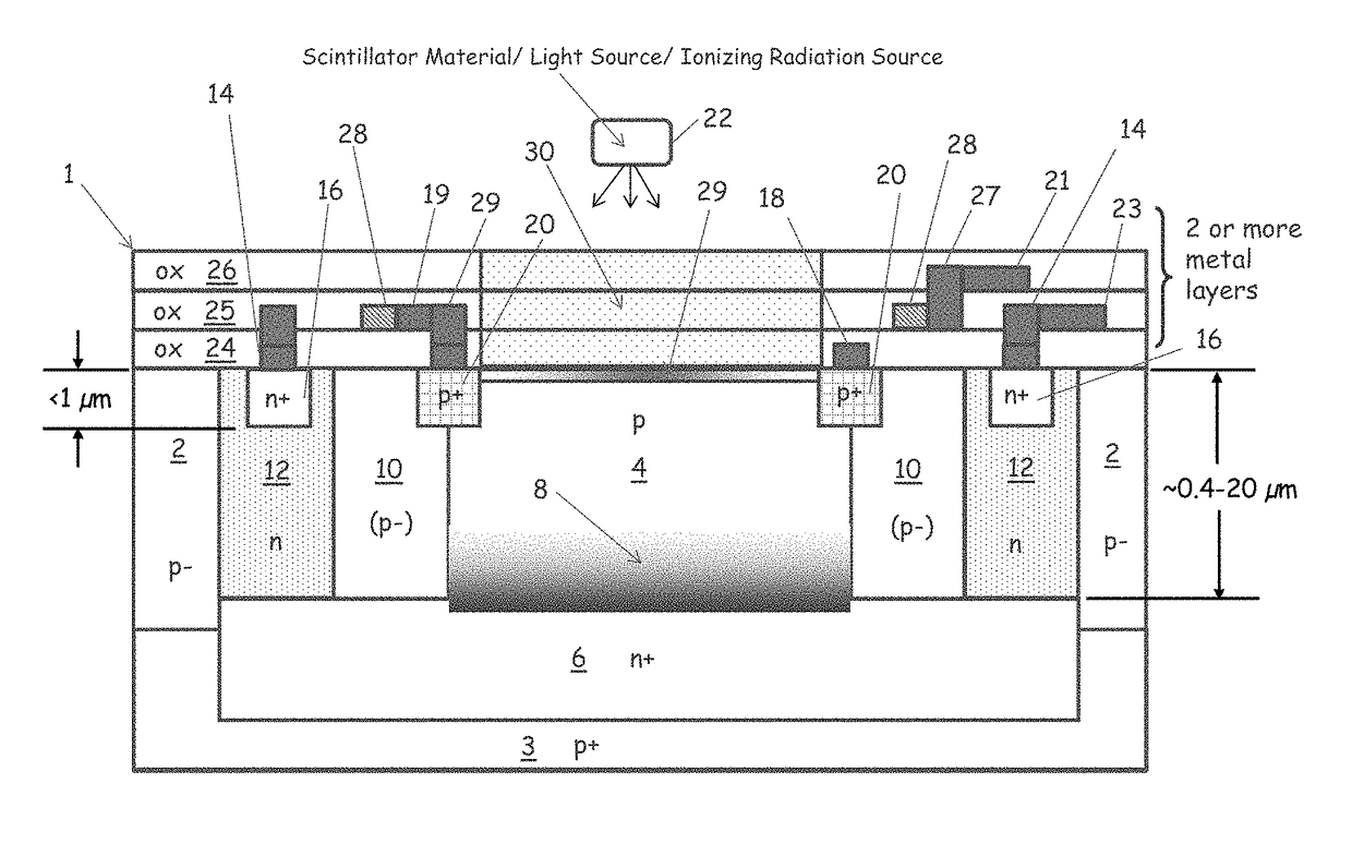
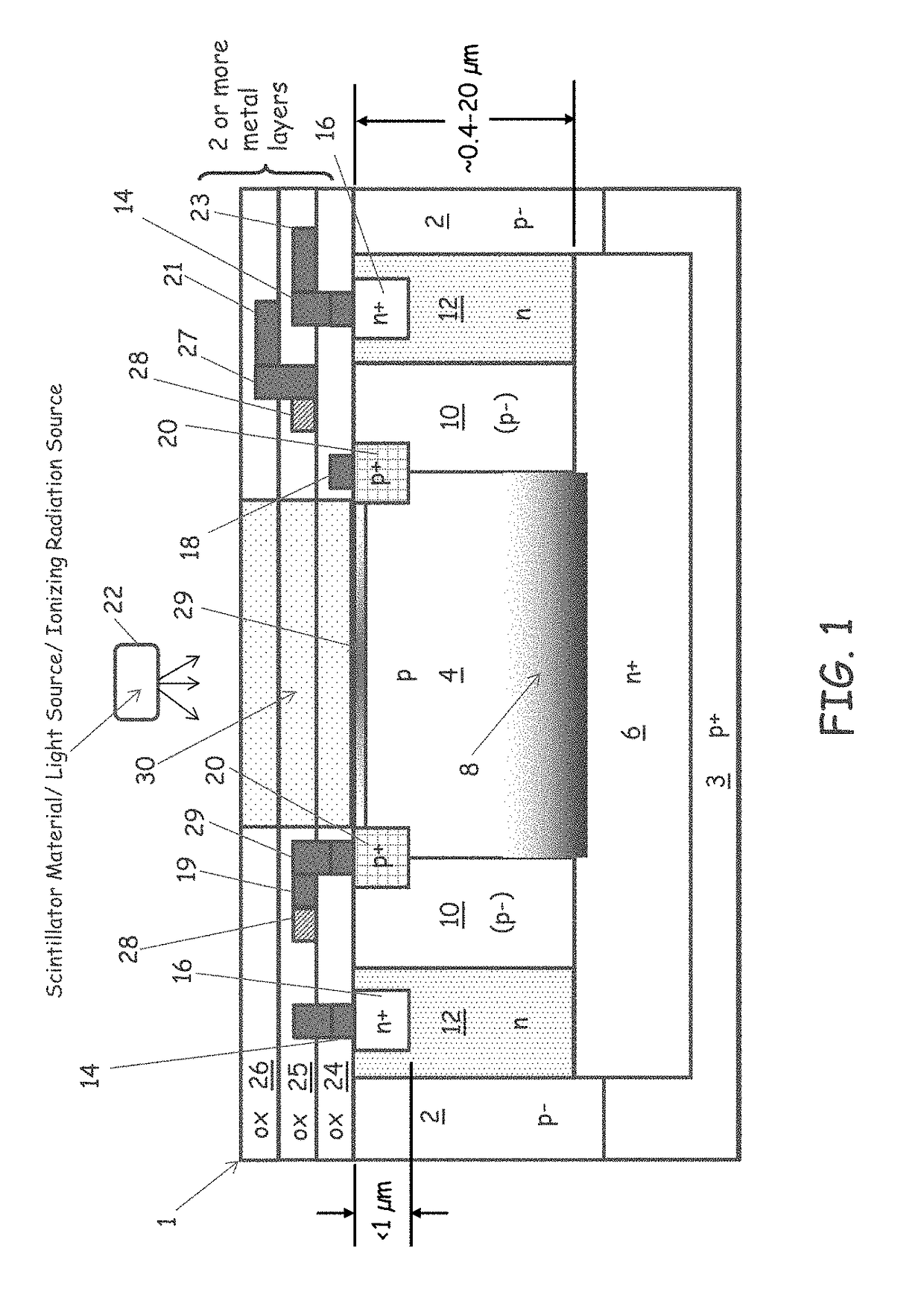
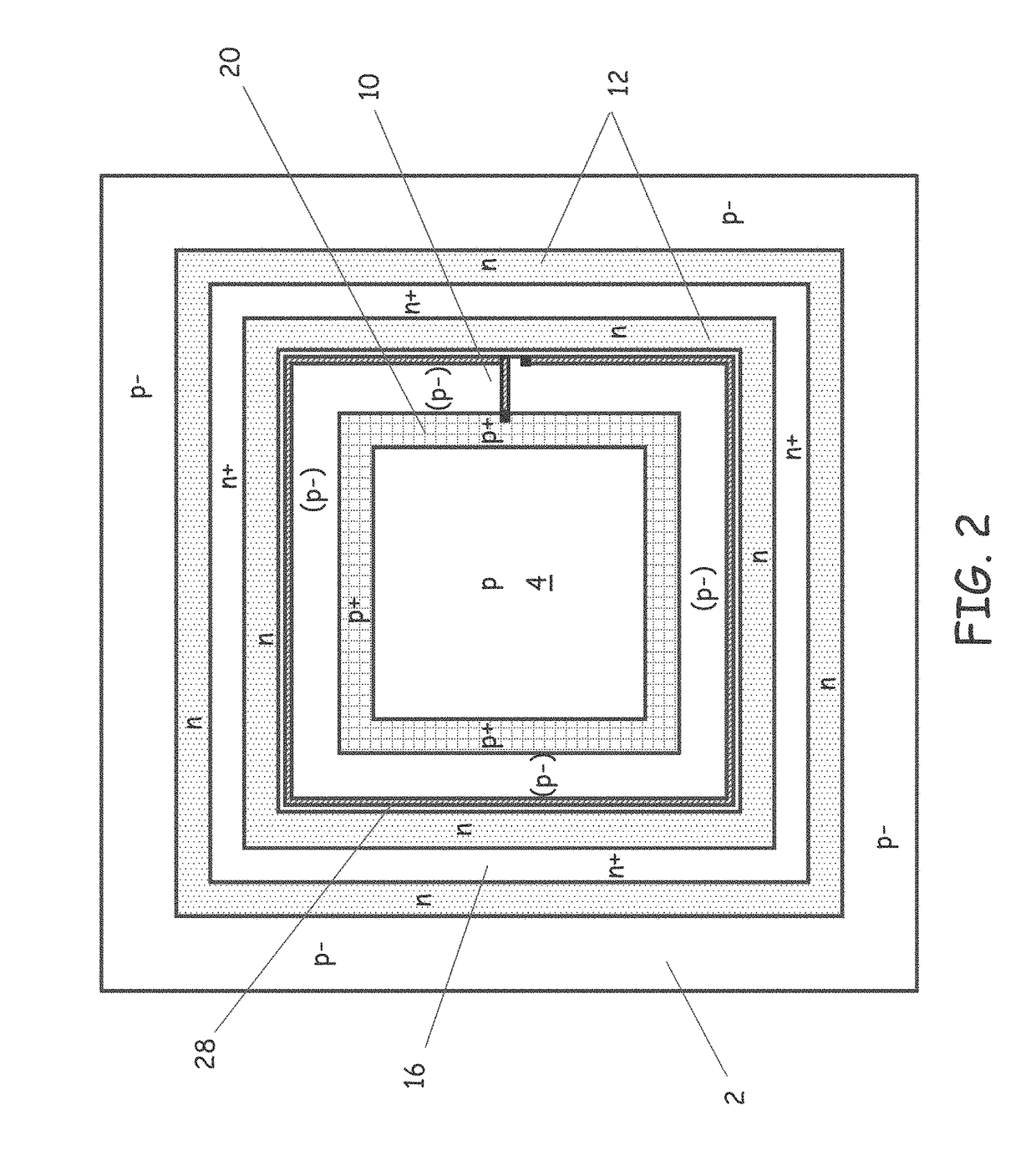
- A photodiode with a buried P-N junction is developed, operated as a Geiger photodiode above its breakdown voltage, forming an array for a solid-state photomultiplier that includes a scintillator material to detect radiation, with a quenching resistor to control avalanches and improve detection efficiency.

Material Science Innovations for Photodiodes
Recent advancements in material science have revolutionized photodiode technology, significantly enhancing device sensitivity and performance. Traditional silicon-based photodiodes are increasingly being supplemented or replaced by novel materials that offer superior optical and electrical properties. Compound semiconductors such as gallium arsenide (GaAs), indium gallium arsenide (InGaAs), and mercury cadmium telluride (HgCdTe) have demonstrated exceptional quantum efficiency across broader spectral ranges compared to conventional silicon.
Nanomaterials represent another frontier in photodiode innovation. Quantum dots, with their tunable bandgap properties, enable precise control over spectral sensitivity. These nanocrystalline semiconductors can be engineered to absorb specific wavelengths, making them ideal for specialized sensing applications. Similarly, two-dimensional materials like graphene and transition metal dichalcogenides (TMDs) offer unprecedented thinness and flexibility while maintaining excellent charge carrier mobility.
Organic semiconductors have emerged as cost-effective alternatives for large-area photodetection. These carbon-based materials can be solution-processed, enabling low-cost manufacturing techniques such as roll-to-roll printing. Recent improvements in organic photodiode stability and quantum efficiency have made them increasingly viable for commercial applications, particularly in flexible electronics and large-area imaging arrays.
Hybrid material systems combine the advantages of different material classes. Perovskite-silicon tandem structures, for instance, leverage the complementary absorption spectra of both materials to achieve broader spectral response. These hybrid approaches often outperform single-material systems in sensitivity tests, particularly when comparing P-N junction characteristics across different material combinations.
Surface engineering techniques have also contributed significantly to photodiode performance enhancement. Anti-reflection coatings, surface passivation layers, and nanostructured light-trapping features minimize reflection losses and surface recombination, thereby increasing quantum efficiency. Advanced doping profiles and heterojunction architectures further optimize charge separation and collection efficiency.
Looking at sensitivity comparisons between traditional P-N junctions and modern photodiode structures, material innovations have enabled dramatic improvements in key performance metrics. Novel materials have achieved up to 30% higher external quantum efficiency, 50% reduction in dark current, and extended spectral response into previously inaccessible wavelength regions. These improvements directly translate to enhanced signal-to-noise ratios and lower detection limits in practical device applications.
Integration Strategies in Optoelectronic Devices
The integration of P-N junctions and photodiodes into optoelectronic systems requires careful consideration of their respective characteristics and performance parameters. When designing integrated optoelectronic devices, engineers must balance sensitivity requirements with spatial constraints and power limitations. The fundamental differences in sensitivity between basic P-N junctions and specialized photodiodes significantly impact integration strategies.
For high-performance applications, photodiodes are typically integrated using flip-chip bonding techniques, which minimize signal degradation by reducing interconnect distances. This approach is particularly valuable when integrating PIN photodiodes with CMOS readout circuits, as it preserves the superior sensitivity characteristics of the photodiode while leveraging the signal processing capabilities of silicon-based electronics.
In contrast, basic P-N junctions may be directly fabricated within existing semiconductor processes, offering seamless integration but with sensitivity trade-offs. Recent advances in monolithic integration have demonstrated P-N junction photodetectors directly incorporated into silicon photonic platforms, achieving reasonable performance despite lower quantum efficiency compared to dedicated photodiodes.
Hybrid integration approaches represent a middle ground, where separately optimized photodiode arrays are attached to application-specific integrated circuits (ASICs) using advanced packaging techniques. This strategy has proven effective in imaging applications where sensitivity requirements vary across the device, allowing designers to incorporate different photodiode structures optimized for specific spectral regions.
The choice between vertical and lateral integration architectures depends largely on the sensitivity requirements revealed through comparative testing. Vertical integration maximizes light collection efficiency but introduces manufacturing complexity, while lateral designs simplify fabrication at the cost of reduced sensitivity. Recent sensitivity tests indicate that vertically integrated photodiodes achieve up to 40% higher responsivity than lateral P-N junctions in the visible spectrum.
Emerging heterogeneous integration platforms are enabling novel approaches that combine III-V photodiodes with silicon photonics, addressing the inherent sensitivity limitations of silicon-based P-N junctions at longer wavelengths. These platforms utilize wafer bonding or micro-transfer printing to place high-performance photodiodes precisely where needed within complex optoelectronic systems.
The integration density achievable with different photodetector technologies directly impacts overall device footprint. While basic P-N junctions offer higher integration density, their lower sensitivity often necessitates additional signal amplification circuitry, potentially negating the space advantage. Sensitivity testing across temperature ranges and operating conditions remains essential for determining the optimal integration strategy for specific applications.
Unlock deeper insights with PatSnap Eureka Quick Research — get a full tech report to explore trends and direct your research. Try now!
Generate Your Research Report Instantly with AI Agent
Supercharge your innovation with PatSnap Eureka AI Agent Platform!